 Open Access Article
Creative Commons Attribution 3.0 Unported Licence
Electrochromic active matrix with plasmonic metasurfaces†
Oliver
Olsson
 *a,
Marika
Gugole
a,
Jolie C.
Blake
a,
Maxim
Chukharkin
b and
Andreas
Dahlin
 a
a
aDepartment of Chemistry and Chemical Engineering, Chalmers University of Technology, 412 96 Gothenburg, Sweden. E-mail: oolsson93@gmail.com
bStiftelsen Chalmers Industriteknik, Sven Hultins Plats 1, 412 58 Gothenburg, Sweden
First published on 28th March 2024
Abstract
Reflective pixels made by plasmonic metasurfaces and tuned by electrochromics exhibit significant potential to be used as flexible, polychromatic, electronic paper. This is attributed to their high reflectivity, low power consumption, and ultrathin dimensions. However, to date, only single pixels of electrochromics combined with plasmonics have been demonstrated. To make a graphical display, pixels in a matrix are required. A matrix configuration that has been successful for emissive displays such as liquid crystal displays (LCD) and organic light emitting-diodes (OLED) is the active matrix. Active matrix configurations consist of thin-film transistors (TFT) in an array where the transistors block unwanted signals. In this study, we demonstrate the suitability of a commercial, flexible TFT array as a substrate for depositing plasmonic metasurfaces in a red, green, and blue subpixel configuration. The conjugated polymer PProDOT-Me2 can be directly polymerized onto selected pixels from a monomer solution and individual pixels can be controlled. We demonstrate the ability of the TFT array to function both in an electrochemical 3-electrode setup and as a 2-electrode flexible device.
Introduction
Electronic paper (e-paper) displays have historically been limited to applications such as e-readers (Amazon Kindle) and electronic shelf labels. Recently, an increased number of advanced technologies have started to incorporate e-paper displays, such as smartphones, with new devices containing e-paper displays being released more frequently. The reason for the heightened interest in e-paper is that it possesses some advantages over conventional (emissive) displays such as liquid crystals (LCD) and organic light-emitting diodes (OLED). E-paper belongs to a category of displays that, instead of generating their own light, rely on ambient light for visibility. The name stems from their reflective nature, and the way a person perceives an image or text is similar to printed materials such as newspapers. Because they do not emit light themselves, e-paper offers reduced energy consumption1 compared to emissive displays. Customers are searching more and more for low power consumption devices, both because of the increasing awareness of the impact energy savings have on sustainability, and to avoid charging devices as often. Furthermore, most e-paper technologies feature bistability, allowing them to maintain the displayed image without consuming additional power, thus further reducing energy consumption.2 This feature is particularly advantageous for displays that do not have to be updated as often, e.g. digital signage advertisements. Electronic paper also provides superior readability3 and its paper-like appearance is gentler on the eyes, which also has been shown to improve sleep quality in comparison with emissive displays.4There is currently no commercial technology for electronic paper in color other than electrophoretic displays (EPDs) like the PocketBook Color.5 EPDs use electrophoretic forces to move pigments, suspended in microcapsules, back and forth into view, turning a pixel black or white. With an additional sub-pixel structure and color filters, the display becomes a color display. Unfortunately, this EPD possesses poor color saturation and a slow refresh rate,5 however, more advanced color EPDs might enter the market in the future.6 The EPD devices on the current market are also very rigid, like most smartphones, and do not possess the flexibility (or bendability) of newspapers and magazines.
Plasmonic color generation7 together with electrochromic materials8,9 has shown promising results for producing e-paper in color by having high non-polarized reflection together with high contrast10 which also (under certain conditions) can be obtained at video rates.11 By depositing metasurfaces and electrochromic materials on a flexible PET substrate the device can be made flexible.12 With high reflection, video speed, and flexibility, plasmonic electronic paper shows a promising technology that can bring the colored electronic papers of today to another level. However, while most research is focused on developing new metastructures or creating novel electrochromic materials, the issue of addressability has been somewhat overlooked. To be able to properly control individual pixels in a pixel-matrix is paramount to taking the leap from material research to high-end technology. Until now, no attempts have been made to use active-matrix technology utilizing commercial TFT arrays (TFT-backplanes) together with both an electrochromic material and plasmonic coloring.
Prior work has utilized plasmonic colors together with a commercial LCD display,13 however, utilizing liquid crystals requires polarized light which significantly reduces the amount of light that can be reflected. Electrochromic materials have the advantage that polarizers are not required to alter their colors. Active matrix displays with electrochromism have been studied before and most recently Bao et al. fabricated a TFT array and deposited various polymers on selective pixels to produce an image.14 However, creating a TFT array from scratch is a cumbersome process that requires in-house semiconductor fabrication techniques. Screen printed carbon nanotubes transistors have been used to create a cheaper and more facile alternative where PEDOT:PSS (polyethylenedioxythiophene:polystyrenesulfonate) was used as the electrochromic material.15 This method, however, lacks full color. Another method is to utilize the semiconducting properties of the electrochromic material PEDOT:PSS to fabricate a printed active matrix display, however, this configuration is also monochromatic and is limited to the use of PEDOT:PSS because of its high intrinsic electric conductive properties.16–18 It should be mentioned that the active matrix configuration is not the only way of making pixelated graphical displays. Passive matrices, which require no transistors, can be utilized, however, pixel confinement is required19 additionally, the electrochromic device also might require a complex electro-optical response to avoid crosstalk.20 To easier transition the colorful plasmonic electrochromic pixels to a practical device, the use of a commercial, pre-made TFT array could greatly decrease the complexity of the manufacturing. Commercial transistors (not TFT) have been used to build basic active matrices with Prussian blue and poly(3-methylthiophene).21 However, no one has combined a commercial backplane with structurally colored pixels for direct switching, i.e. without the use of liquid crystals.
With this work, we want to demonstrate that it is indeed feasible to prepare highly reflective metasurfaces on a flexible commercial TFT substrate. We present how plasmonic structures can be readily deposited on this flexible commercial TFT array using standard vacuum processes and parallel lithography. We also show that an electrochromic polymer can be synthesized directly on top of the pixels by electropolymerization. This gives the opportunity to easily synthesize the appropriate electrochromic materials on different pixels to enhance the performance of the colored metasurface.22
Results and discussion
Active matrix functionality
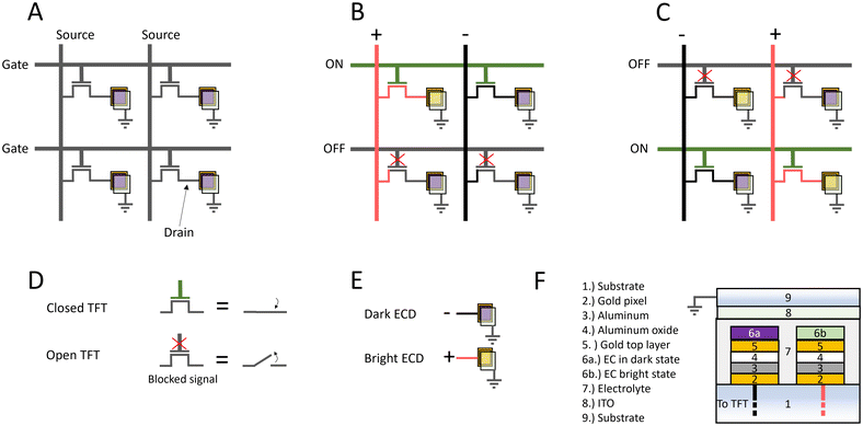
To fully appreciate the importance of utilizing an active matrix configuration, its working principle will first be presented. A grid of pixels where each pixel is connected to a TFT builds up a two-dimensional matrix. One TFT has three terminals: source, drain, and gate. The voltage on the gate controls the current that can pass between the source and drain. A schematic of a 2 × 2 matrix can be viewed in Fig. 1A where every gate on one row is connected and every source on each column is connected. Each drain is connected to the pixel which is visible to the viewer. The TFT's can be viewed as switches, which are either closed (ON) and conducting electricity, or open (OFF) and not conducting electricity (Fig. 1D). In this example, the electrochromic pixels are either in their bright state (pixel ON) or dark state (pixel is OFF) (Fig. 1E). Fig. 1B shows how only the top left pixel is switched by biasing the left source line with a positive voltage while closing the gates on the top row. This will change the color of the top left pixel from a dark state to a bright state while leaving the lower left pixel unaffected since the TFT's on that row are open (OFF). Subsequently, by opening the top row and closing the bottom row we can change the color of the bottom right pixel by applying a positive voltage to the right source line (Fig. 1C). This is only an example and if the aim is to change the color from dark to bright of both the bottom pixels a positive bias would have to be applied to both sources. The pixels in the top row will retain their color due to either bistability or an incorporated storage capacitor (built in the backplane) connected between the drain and ground (parallel to the device). With m number of rows and n number of columns the total amount of connections that are required for this configuration is m + n. If, instead, each pixel would be directly addressed the displays would require m × n connections. For a simple VGA graphic standard, where the resolution is maximum 640 × 480 means that 307![[thin space (1/6-em)]](https://www.rsc.org/images/entities/char_2009.gif) 200 connections are required if each pixel is directly addressed, which is not feasible to fabricate nor to operate. This number significantly reduces to merely 1120 when utilizing the a matrix configuration.23
200 connections are required if each pixel is directly addressed, which is not feasible to fabricate nor to operate. This number significantly reduces to merely 1120 when utilizing the a matrix configuration.23
Fig. 1F shows a cross section schematic of two plasmonic electrochromic pixels on a substrate. The metasurface consists of a metal–insulator–metal (MIM) layer to create a Fabry–Pérot cavity which can reflect a defined part of the visible spectrum. Nanoholes are introduced into the top metal to create a plasmonic effect that scatters red light and thus enhances the saturation of the blue and green pixels.24,25 The electrochromic material is deposited on top of the metasurface and can then tune the reflection by altering its transparency. It should be noted that the electrochromic material requires an electrolyte to be able to switch color.10
Nanofabrication
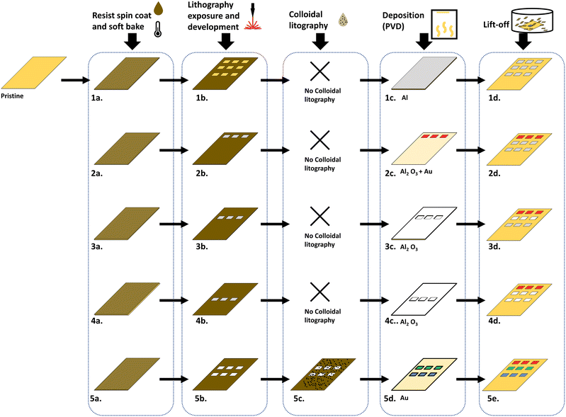
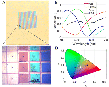
The plasmonic metasurfaces were prepared upon a commercial flexible PET-based TFT array (4′′, 240 gates and 400 sources) from Plastic Logic. The TFT arrays were delivered with gold-plated top electrodes (pixels) with dimensions of 200 × 200 μm2. The space between each pixel was 20 μm which gives a fill factor of 82%. The metasurface consists of an aluminum mirror, aluminum oxide with varying thicknesses, and a gold reflector.10 The color of the metasurface stems from Fabry–Pérot resonance created by this metal–insulator–metal (MIM) structure. Green and blue pixels have a nanohole array on the top gold electrode to generate a plasmonic effect for enhanced coloration by scattering red light. The RGB surfaces were fabricated for each pixel by previously described methods10 with multiple additional lithography steps (Fig. 2). Thermal tape (120 °C) was used to fix the PET-based TFT arrays to a silicon wafer which served as a platform to stabilize and isolate the arrays during the lithography steps. The bottom aluminum mirror is common for every color and was first deposited on every pixel using laser writing and lift-off in acetone (Fig. 2 step 1a–d). Before the lift-off, the tape was completely removed by heating the substrate for ∼10 second long intervals on a hotplate at 120 °C (if the substrate was heated continuously at 120 °C, the PET started to deform). After each lift-off, a new tape was reapplied to fix the substrate to the silicon wafer. The red pixel was then created on one-third of the pixels by repeating lithography with 65 nm evaporated aluminum oxide and 20 nm gold (Fig. 2 step 2). Aluminum oxide was then deposited on one-third of the pixels with a layer of 95 nm (Fig. 2 step 3) for the green pixel's spacer layer. Subsequently, 110 nm is deposited on the remaining third of pixels (Fig. 2 step 4) to make the blue pixels. An additional step of colloidal lithography was required before depositing the top gold layer on the green and blue pixels (Fig. 2 step 5d).All three colors were fabricated on a cut-out piece of the backplane (Fig. 3A) and microscope images (4×) revealed that the metasurfaces were well aligned on the TFT's top pixels (albeit made slightly smaller due to the tolerance of the laser writer) (Fig. 3C). The reflection spectra of the single pixels collected at 40× magnification (Fig. 3B) show that the individual pixels have a high peak reflectivity (>80%). A spectrum of the full surface (RGB) with an exposed area of 1 cm2 is included which proves that the resulting color is, as expected, white. Fig. 3D shows the CIE chromaticity coordinates of the individual metasurfaces (black circles) and the full subpixel structure (white ring). The colors enclosed within the triangle are secondary colors that can be produced by modulating the brightness of the three pixels. Compared to previously reported values, by our group, for similar surfaces, the reflection peaks are slightly blue-shifted.10 This could be because the deposition of the spacer layer by evaporation has some variance. However, if the variance is the same for every color, which is the case, the CIE triangle will be rotated. This will not alter the area of the triangle significantly and have a minor impact on the number of secondary colors that can be produced.
Polymers on TFT arrays
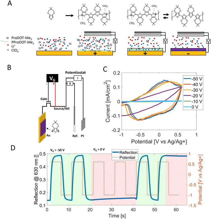
To be able to turn the pixels ON and OFF (high reflection or low reflection) the polymer poly(2,2-dimethyl 3,4-propylenedioxythiophene) (PProDOT-Me2) was chosen as the electrochromic material. We have previously described how to synthesize PProDOT-Me2 on both planar gold and nanostructures with excellent contrast (77% at λ = 580 nm) and reproducibility by electropolymerization.10 This method gives the opportunity to synthesize the polymer directly upon the desired surface. By applying a positive potential to the electrode immersed in a monomer-containing electrolyte, the polymer grows on the surface until a continuous film with a desired thickness is formed. The polymer is deposited in its ion-doped bright state (transparent). The dark state (opaque) can be obtained by applying a negative potential and effectively dedoping the polymer of ions (Fig. 4A).10,26 The electropolymerization was performed in a flow cell or a custom-made glass vessel, both filled with electrolyte (0.1 M LiClO4 – propylene carbonate) and 10 mM monomer. As described previously, each pixel on the array is connected to a TFT (thin-film transistor). This transistor can be opened (OFF) or closed (ON). The TFT array had two kinds of terminals: source lines connected to the top pixel through the transistors, and gate lines that control the thin film transistors. The fan-out of the source and gate terminals had a pitch of 20 μm which was too fine to manually contact, thus connections to individual pixels were not done in this step. The polymer was, instead, deposited on bundles of pixels. Bundles were created by using silver glue to connect gate terminals together and source terminals together. The transistor gates were controlled by a separate power source in a common source configuration: the negative terminal was connected to the transistor gate lines, and the positive terminal was connected to the potentiostat working electrode – the source lines. A built-in storage capacitor was left floating (not connected). A voltage of around −50 V was used to close the gates (ON) and allow the potentiostat to drive current through the transistors. The schematic is shown in Fig. 4B. Cyclic voltammetry has shown to be a reliable method for electropolymerizing PProDOT-Me2 which gives full control of the thickness of the film,10 however, it requires careful control of the working electrode to a reference electrode thus a three-electrode configuration is necessary. A potentiostat was used in a three-electrode setup with the working electrode connected to the source lines, the counter electrode was a platinum coil/net or ITO-plastic, and the reference electrode was a commercial silver reference (Ag/Ag+). Polymerization onset occurred at a similar potential as previously reported10 but the current density during the polymerization was lower for the TFT array compared to a gold-coated glass substrate (S1A) and the cyclic voltammetry was swept to higher potentials (+1.3 V vs. Ag/Ag+) than previously used. This trait can be attributed to higher resistance in the TFT array than for the directly contacted gold surface. Polymerization was conducted utilizing a charge consumption of ∼10 mC cm−2 which generates a high contrast and has a thickness of ∼75 nm.10Switching characteristic
TFT displays are updated row by row. Each row has its gates open (ON) for a certain amount of time while signals (voltage) are applied to all columns to update the pixels on the selected row. After the selected row has been updated the row is opened (OFF) and the next row is selected. To avoid cross talk it is important that when the gates are opened (OFF) the pixels should be unaffected by applied potentials. Fig. 4D shows the reflection trace while potentials of −1 V and +0.6 V are applied. Keeping the gate at −50 V (shaded green) allows the polymer to switch between its dark and bright state. When turning the gates off by applying 0 V to the gate (short-cut), the applied potentials from the potentiostat are blocked (red-shaded) and the polymer does not alter its optical state. Similarly, cyclic voltammetry shows no current when the gate voltage is 0 V (Fig. 4C). The voltammogram exhibits the characteristic current shape of a conjugated polymer when the gate voltage is decreased to −50 V, further validating that the TFT's acts as low-resistant wire. A further separation between the reduction peak and the oxidation peak is visible at gate voltages of −40 V and −30 V (increasing the gate voltage to positive voltages was possible). This peak separation is characteristic of an increasing resistance of either the electrolyte or the electrode. Comparing the TFT-pixel to a 100 nm gold surface on a glass, the potentials for the TFT array already exhibit some separation when the gates are biased with −50 V (S1B). It is most likely because the resistances in the TFT configuration cannot be zero, even when the gate voltage is −50 V. By decreasing the scan rate the current is also lowered, which also decreases the voltage drop over the resistance and the peak separation of the TFT vanishes (S1C). We also constructed a simple automatic driving circuit to show that it is indeed feasible to change the color of different bundles of pixels (ESI & SI Movie†). Some initial attempts to utilize a built-in capacitor (storage capacitor) were conducted. We saw no difference in the switching time, however the bistability time for the dark state (5% contrast loss) was reduced from 62 s without the capacitor to 3 s with capacitor. The bright state bistability was more than 300 s (longer than the experiment) without the capacitor and 40 s with the capacitor (ESI†).Optical properties
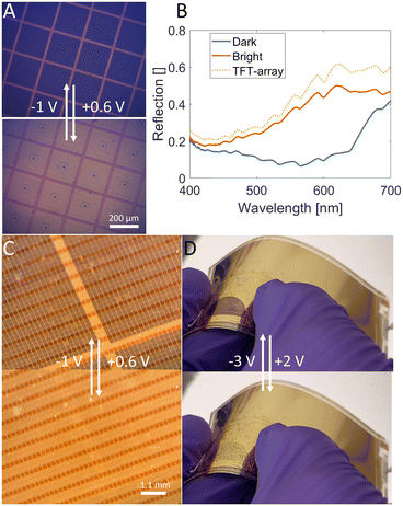
Microscope images of PProDOT-Me2 deposited on the gold pixels show that, as expected, polymerization occurs only at pixel electrodes (Fig. 5A) and no unwanted polymerization occurs between pixels. The maximum contrast (reflection difference) is 37% at 630 nm which is lower than if only the polymer's contribution was considered (Fig. 5B). We attribute the lower reflection and contrast to both the fill factor (0.82) and that the in situ electrochemical setup reduces reflection by around 25%, as previously reported by our group.5 The red metasurface was deposited on one third of the pixels of a backplane and polymerization was successfully performed on bundles of pixels. Fig. 5C shows the switching of the polymer on top of the red metasurface. The electrical connection between the TFT and the top layer of the metasurface should theoretically be blocked because of the insulating aluminum oxide layer. However, because of the very thin layer of the insulator and the limitations of the PVD there are most likely some stray connections between the aluminum and the gold throughout the pixel. Another factor is the limitations of the laser writer which could make the top gold slightly overlap with the TFT-gold electrode. We want to stress that all experiments are done on a PET-substrate. This opens the possibilities for making flexible electronic paper which is important for mimicking ordinary newspaper. We demonstrate this in Fig. 5D where one part of the TFT array has been made into a device (2-electrode setup) and switched while being bent.Polymerization and switching on selected pixels
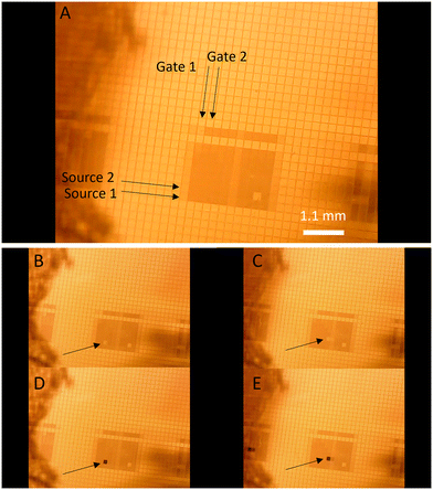
To show that it is indeed possible to control selected pixels, wire bonding was chosen as a method to individually contact the terminals for both the source and the gate lines. A schematic and details of the bonding can be viewed in S4. Polymerization was made “gate wise” i.e. all gates were opened (OFF) with +20 V (the gates remained opened after the +20 V were disconnected). The first selected gate line was closed (ON) with −50 V while the potentiostat was applying a potential on the 10 source lines. Subsequently, the first gate line was opened (OFF) and the next gate line was closed (ON) and polymerization was performed on the same 10 source lines. This process was repeated for the remaining 8 bonded gates and resulted in a square (10 × 10) of deposited polymers on the TFT backplane (Fig. 6A). Gate line 6 and source lines 8 and 10 didn't have proper contact which resulted in a lack of polymer. There also seem to be some unwanted polymers on the adjacent gates next to the first and the last (gate line 0 and 11) which also could be due to short circuits from the wire bonding. Even though the polymerization isn't perfect it still demonstrates the power of electropolymerization since the polymers can be directly synthesized on selected pixels and without additional patterning methods utilizing the intrinsic patternability of the TFT matrix itself. Many electrochromic materials exhibit a good contrast in different parts of the visible regime, so the most suitable material for e.g. red pixels is not necessarily the most suitable for blue pixels.22 Direct synthesis of polymers on the pixels provides an easy method to use different materials for different pixels. Another important factor is cross talk during switching. When one-pixel switches, the unaddressed pixels should not switch. Fig. 6B–E shows switching on individual pixels with little to no cross talk between neighboring pixels. It should be noted that the electrolyte is global, and the different pixels were in fact ionically connected, nevertheless, they can be separately addressed. The total time of one switch (colored to bright and back) was approximately 1 second. Although some pixels were not completely free of cross talk (ESI† Movie), it was likely caused by shortcuts in wire bonding.Conclusions
We have presented how plasmonic metasurfaces can be prepared on a PET-based flexible commercial TFT matrix with standard lithography and evaporation methods. An electrochromic polymer could then be electrodeposited on the metasurfaces. We have shown that it is indeed possible to use a TFT matrix to not only block and admit currents for an electrochromic material, but also for vital electrochemical experiments such as cyclic voltammetry. This could potentially open this technology to applications other than displays, such as multi electrode electrochemistry sensors, like biosensors.14 The polymer could be switched while the matrix was being bent which illustrates that the flexible PET properties can be transferred into a complete device. The polymer could be polymerized on selective pixels and individually switched without any cross talk, corroborating that the TFT matrix technology can indeed be used with electrochromic polymers.Future endeavors would consist of evaluating the lifetime of the polymer on TFT's in terms of the number of switches and how the bending of the TFT device would affect the lifetime. To realize a functioning electronic paper device, commercial driving circuits have to be utilized. Backplanes with mounted driving circuits would get rid of the “bonding problem”. Further, different backplane technologies could be tested. Different display technologies require different TFT backplanes: OLED displays do not use the same backplane as LCD displays. Another commercial backplane might have a pixel storage capacitor more suitable for this application to reduce the switching time. However, even if the backplane used in this study was not made to be used with our technology, we have demonstrated that our electrochromic plasmonic metasurfaces can be both fabricated and switched. This shows a promising aspect of commercialization of electrochromic plasmonic metasurfaces.
Experimental
Nanofabrication
Patterning of the metasurfaces on top of the TFT-backplanes was made by laser lithography (Heidelberg Instruments DWL 2000). The backplane was fixed to a silicon wafer with thermal tape. The photoresist (AZ1512HS) was spin coated at 4000 rpm and soft baked on a hotplate at 85 °C for 2 min. A 60 mW laser exposed the pixels and the backplane was developed in MF-318 for 50 s. To create a metasurface Al (with 5 nm Cr adhesion layer), Al2O3, and Au (with 1 nm Ti adhesion layer) were deposited by evaporation (Lesker PVD 225). For green and blue pixels, prior to Au deposition, colloidal lithography was performed with 147 nm polystyrene-sulphate particles.Polymer deposition
For electropolymerization on the backplane a silver glue (Loctite) was deposited on all/or bundles of the source and gate lines. For in situ optical measurements, the backplane was inserted in an electrochemical flow cell (RedoxMe). For deposition on individual pixels of larger areas, a homemade vessel was made by gluing together cut out glass pieces with epoxy glue. The backplane was attached to another glass piece and inserted into the vessel. The gates were connected to the negative terminal of a variable power supply (RSPro DF1760SL3A), while the positive terminal was connected to the source lines. A potentiostat (Gamry Reference 600+) was connected to the setup. The working electrode was connected to the source line, the counter electrode was connected to either a platinum-net or ITO plastic and the reference electrode was a commercial Ag/Ag+ (RedoxMe, Ag-wire in 0.1 M acetonitrile, 0.01 M AgNO3). The reference and the counter electrode were placed inside the vessel together with the backplane. Polymerization of PProDOT-Me2 was done in propylene carbonate with 0.1 M LiClO4 (Sigma Aldrich) with 0.01 M ProDOT-Me2 (Sycon Polymers). The gates were closed (ON) by applying −50 V. When the gates were pulsed, a mechanical relay was used to either connect the gate to 0 V or −50 V. Polymerization was performed with cyclic voltammetry (100 mV s−1) between −1 V and 1.3 V as previously described.10 Wire bonding was used to selectively bond individual source and gate lines to a gold-plated PCB. The substrate was fixed to the PCB before wire bonding with double-sided adhesive. The wire was made of gold and the bonds were glued for rigidity.Flexible device fabrication
0.1 M LiClO4 in PC was mixed with a binder (PVDF-TrFE; 70![[thin space (1/6-em)]](https://www.rsc.org/images/entities/char_2009.gif) :
:![[thin space (1/6-em)]](https://www.rsc.org/images/entities/char_2009.gif) 30) and stirred with heating (100 °C) for 60 min and then mixed again using a SpeedMixer DAC (Hauschild). The electrolyte was then smeared on both the TFT array and the ITO plastic and left on an 80 °C hot plate for ∼5 min. When some of the solvent had evaporated and the remaining electrolyte was still warm the two substrates were laminated by hand and left to cool. To fully switch the polymer a voltage of −3.5 V to +2.5 V was used.
30) and stirred with heating (100 °C) for 60 min and then mixed again using a SpeedMixer DAC (Hauschild). The electrolyte was then smeared on both the TFT array and the ITO plastic and left on an 80 °C hot plate for ∼5 min. When some of the solvent had evaporated and the remaining electrolyte was still warm the two substrates were laminated by hand and left to cool. To fully switch the polymer a voltage of −3.5 V to +2.5 V was used.
Optical measurement
The sample was illuminated by a tungsten lamp (Azpect Photonics) using a homemade microscopy/reflection setup. The reflected light was collected with an objective (Olympus, 40× air NA 0.1 for the single metasurface pixels or 4× for in situ measurements) and guided to a spectrometer (B&WTek). The dark counts in the detector were always subtracted from the measured intensities. A homemade silver mirror was used as a reference in the flow cell. And the homemade mirror was later compared to a commercial dielectric mirror (BB05-E02, Thorlabs). The area-averaged RGB sample was measured with a spectrophotometer (Konica Minolta CM-700d, 1 cm2 exposed area).Driving circuit
The driving circuit was made with an Arduino-controlled potentiostat27 interfaced with LabView. The working electrode was multiplexed (MUX, CD4051BG). P-channel MOSFETs (J9A10M3) were used to set the gate voltage. These MOSFETS can simultaneously distribute the voltage provided by the power supply to the gate lines of the backplane and turn the thin-film transistors ON and OFF. The Arduino (UNO 3) is also controlling the potentiostat which can distribute the desired potential to multiplex. The multiplex, likewise controlled by the Arduino, opens and closes the terminals from the potentiostat to the desired source lines one by one.Author contributions
OO performed most of the experiments including electrochemical experiments and optical measurements. MG and JCB performed all nanofabrication. MC performed wire bonding. The project was led by O. O. together with A. D. The manuscript was written by O. O. with support by A. D. and input from all authors.Conflicts of interest
There are no conflicts to declare.Acknowledgements
Dr. Kunli Xiong is acknowledged for conceptualized the idea. Dr. Peter Andersson Ersman at RISE is acknowledged for useful discussions. We thank Ioannis (Yiannis) Petsagkourakis at RISE for formulating and mixing the PVDF electrolyte. This work was performed in part at MyFab Chalmers. This work was financed by the Swedish Foundation for Strategic Research (EM16-0002).Notes and references
- P. F. Bai, R. A. Hayes, M. Jin, L. Shui, Z. C. Yi, L. Wang, X. Zhang and G. Zhou, Prog. Electromagn. Res., 2014, 147, 95–116 CrossRef.
- M. Fernández, E. Casanova and I. Alonso, Sustainability, 2015, 7, 10854–10875 CrossRef.
- S. Benedetto, V. Drai-Zerbib, M. Pedrotti, G. Tissier and T. Baccino, PLoS One, 2013, 8, e83676 CrossRef PubMed.
- A.-M. Chang, D. Aeschbach, J. F. Duffy and C. A. Czeisler, Proc. Natl. Acad. Sci. U. S. A., 2015, 112, 1232–1237 CrossRef CAS PubMed.
- M. Gugole, O. Olsson, S. Rossi, M. P. Jonsson and A. Dahlin, Nano Lett., 2021, 21(10), 4343–4350 CrossRef CAS PubMed.
- E. Huitema and I. French, IEEE Spectrum, 2022, 59, 30–35 Search PubMed.
- K. Xiong, D. Tordera, M. P. Jonsson and A. B. Dahlin, Rep. Prog. Phys., 2019, 82, 024501 CrossRef CAS PubMed.
- C. Gu, A.-B. Jia, Y.-M. Zhang and S. X.-A. Zhang, Chem. Rev., 2022, 122, 14679–14721 CrossRef CAS PubMed.
- L. Huang, S. Cao, Y. Liang, J. Chen, T. Yang, J. Zhao and B. Zou, J. Mater. Chem. C, 2023, 11, 10107–10120 RSC.
- M. Gugole, O. Olsson, K. Xiong, J. C. Blake, J. Montero Amenedo, I. Bayrak Pehlivan, G. A. Niklasson and A. Dahlin, ACS Photonics, 2020, 7(7), 1762–1772 CrossRef CAS.
- K. Xiong, O. Olsson, J. Svirelis, C. Palasingh, J. Baumberg and A. Dahlin, Adv. Mater., 2021, 2103217, DOI:10.1002/adma.202103217.
- K. Xiong, D. Tordera, G. Emilsson, O. Olsson, U. Linderhed, M. P. Jonsson and A. B. Dahlin, Nano Lett., 2017, 17, 7033–7039 CrossRef CAS PubMed.
- D. Franklin, R. Frank, S.-T. Wu and D. Chanda, Nat. Commun., 2017, 8, 15209 CrossRef PubMed.
- B. Bao, B. Rivkin, F. Akbar, D. D. Karnaushenko, V. K. Bandari, L. Teuerle, C. Becker, S. Baunack, D. Karnaushenko and O. G. Schmidt, Adv. Mater., 2021, 33, 2101272 CrossRef CAS PubMed.
- X. Cao, C. Lau, Y. Liu, F. Wu, H. Gui, Q. Liu, Y. Ma, H. Wan, M. R. Amer and C. Zhou, ACS Nano, 2016, 10, 9816–9822 CrossRef CAS PubMed.
- J. Kawahara, P. A. Ersman, D. Nilsson, K. Katoh, Y. Nakata, M. Sandberg, M. Nilsson, G. Gustafsson and M. Berggren, J. Polym. Sci., Part B: Polym. Phys., 2013, 51, 265–271 CrossRef CAS.
- P. Andersson, R. Forchheimer, P. Tehrani and M. Berggren, Adv. Funct. Mater., 2007, 17, 3074–3082 CrossRef CAS.
- P. A. Ersman, R. Lassnig, J. Strandberg and P. Dyreklev, Adv. Eng. Mater., 2021, 23, 2000771 CrossRef.
- C. Gu, Y. Yan, J. He, D. Pu, L. Chen, Y.-M. Zhang and S. X.-A. Zhang, Device, 2023, 1, 100126 CrossRef.
- P. A. Ersman, K. Freitag, J. Kawahara and J. Åhlin, Sci. Rep., 2022, 12, 10959 CrossRef PubMed.
- D. S. Kim, H. Park, S. Y. Hong, J. Yun, G. Lee, J. H. Lee, L. Sun, G. Zi and J. S. Ha, Appl. Surf. Sci., 2019, 471, 300–308 CrossRef CAS.
- O. Olsson, M. Gugole and A. Dahlin, Nanophotonics, 2023, 12(8), 1591–1599 CrossRef.
- Handbook of Visual Display Technology, ed. J. Chen, W. Cranton and M. Fihn, Springer-Verlag Berlin Heidelberg, 2012 Search PubMed.
- Y. Liu, L. Huang, S. Cao, J. Chen, B. Zou and H. Li, Nanophotonics, 2024, 13, 155–172 CrossRef CAS.
- K. Xiong, G. Emilsson, A. Maziz, X. Yang, L. Shao, E. W. H. Jager and A. B. Dahlin, Adv. Mater., 2016, 28, 9956–9960 CrossRef CAS PubMed.
- G. Sabouraud, S. Sadki and N. Brodie, Chem. Soc. Rev., 2000, 29, 283–293 RSC.
- G. N. Meloni, J. Chem. Educ., 2016, 93, 1320–1322 CrossRef CAS.
Footnote |
| † Electronic supplementary information (ESI) available. See DOI: https://doi.org/10.1039/d3lf00266g |
| This journal is © The Royal Society of Chemistry 2024 |

