 Open Access Article
Current induced cooling in a metal/n-InAs structure
N. D.
Il'inskaya
a,
S. A.
Karandashev
a,
T. S.
Lukhmyrina
 a,
B. A.
Matveev
*a,
M. A.
Remennyi
a and
A. E.
Chernyakov
b
aIoffe Institute, St. Petersburg, 194021, Russia. E-mail: bmat@iropt3.ioffe.ru
bSubmicron Heterostructures for Microelectronics Research and Engineering Center of the Russian Academy of Sciences, 194021, St. Petersburg, Russia
First published on 30th April 2024
Abstract
This paper focuses on the specific features of an Ohmic contact on undoped n-InAs (n = 2 × 1016 cm−3) that could be used for temperature stabilization and/or temperature reduction in electronic devices, mainly operating in the 3–5 μm mid-IR range. This feature has been demonstrated in a 100 μm thick n-InAs slab with three unannealed Cr–Au–Ni–Au contacts formed via evaporation in vacuum. The I–V characteristics showed no deviation from Ohm's law in the temperature range 77–340 K, manifesting a contact resistance ranging from 3.6 × 10⁻⁵ to 7.2 × 10⁻⁵ Ω cm2 at room temperature. The 2D thermal radiation distribution and the temperature distribution over the n-InAs surface opposite the contact side surface was obtained via a pre-calibrated IR microscope operating at a wavelength of 3 μm. The measurements revealed a current dependent temperature decline in the area adjacent to the negatively biased contact: at the applied power of 5 mW, cooling as strong as ΔT ≈ 1 K occurred at an ambient temperature of 340 K. The results show potential for the fabrication of heterostructures with a “built-in” cooler that is monolithically integrated with another electronic device.
Introduction
Electrically driven solid state refrigeration has been known for more than a century, and Peltier coolers are now used in a variety of applications. Nevertheless, the demand for low-power on-chip devices for many applications1,2 is one of the most significant demands of this decade, including coolers that are monolithically integrated into them. Therefore, the need for a compact and efficient miniature “heat pump” for electronic components strongly encourages the investigation of electrocaloric materials3 and p–n structures, e.g. at a forward bias (FB). Previous research has reported opto-thermionic refrigeration,4 thermophotonic heat pumping,5 thermo-electro-photo cooling,6 electroluminescent refrigeration,7 and electroluminescent cooling,8 all referring to electronic cooling in FB p–n heterostructures. An alternative to the above approach employs the negative luminescence (NL) phenomenon in narrow-gap semiconductors activated by the magnetoconcentration/galvanomagnetic effect or by a reverse biasing of p–n structures.9–12 The corresponding heat engine ability has been referred to as a “radiative cooling effect due to negative luminescence”13 or “photonic cooling through the control of the chemical potential of photons”14 and has been used in experiments with spatially separated NL devices and an object to be cooled.All the above-mentioned semiconductor devices utilize metal/semiconductor (MS) junctions as a source of non-equilibrium charge carriers that enter or leave the semiconductor body. In most cases, these junctions, including the Me/n-InAs junction,15,16 were considered as Ohmic electrical contacts—in other words, potential sources of Joule heat. This may not be fully true as an MS interface with certain parameters is capable of producing the cooling of a contact area at a negative bias on the metal.17 However, to the best of our knowledge, there have been no attempts to test the potential cooling ability of the Me/n-InAs junction.
In this paper, we demonstrate that the current flow through the Ohmic contact at the Me/n-InAs junction leads to the cooling effect instead of Joule heating.
Materials and methods
The sample consists of a p-InAsSb (3 μm thick)/n-InAsSb (3 μm thick) heterostructure (HS) grown using the LPE method onto an undoped n-InAs (100) substrate cut from a Czochralski ingot fabricated via GIREDMET.18Table 1 summarizes the parameters of the ingot (substrate mother) as declared by the manufacturer's certificate.| Parameter | Ratings | Units |
|---|---|---|
| Bulk resistance, 77 K | (5.98–5.72) × 10−3 | Ω cm |
| Free electron concentration, 77 K | (2.17–2.28) × 1016 | cm−3 |
| Dislocation density | (1.6–3) × 104 | cm−2 |
The transmission spectrum shown in Fig. 1 is typical for the undoped n-InAs, as it suggests a lack of significant free electron absorption at long wavelengths. Also shown in Fig. 1 is an IR microscope responsivity spectrum, i.e. the spectrum of the cooled InAs detector developed at the Institute of Semiconductor Physics, the Siberian Branch of the Russian Academy of Sciences,19 which provided 128 × 128 px (2 × 2 mm) radiation intensity maps of the sample under study. As seen from the data in Fig. 1, the microscope sensitivity subsides at around 3 μm so that the substrate transmission and microscope responsivity have poor overlapping. Therefore, we were able to measure the purely thermal radiation as well as the temperature distribution over the n-InAs surface without the concern of detecting some kind of electroluminescence that could potentially arise from radiative recombination near the Me/n-InAs interface. The 2D temperature distribution was estimated utilizing calibration curves that were experimentally derived using the same sample under study at T = 300–370 K.
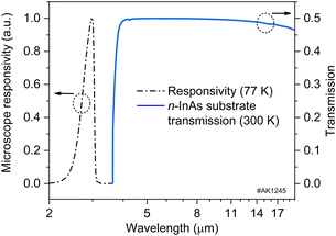 | ||
| Fig. 1 Spectral responsivity of the IR microscope/camera at 77 K (left scale) and the estimated optical transmission of a 100 μm-thick n-InAs substrate (right scale). | ||
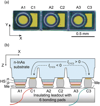
The sample was a “troika of diodes” (a 1 × 3 linear array) with three 30 μm high circular mesas (Øm = 190 μm), ∼50 μm deep separation grooves, three circular Cr–Au–Ni–Au based anodes (A1, A2 and A3) (ØA = 170 μm) and three Cr–Au–Ni–Au cathodes (C1, C2 and C3) of nearly rectangular shape formed by evaporation in vacuum and a standard photolithography process and wet chemical etching so that the n-InAs (100) substrate surface was free of contacts as in previous reports.16,20 No annealing was used while preparing the contacts. Fig. 2 shows the troika cross section schematic, where a 7.1 × 7.1 mm AlN leadout with six bonding pads provided an electrical connection to the troika contacts. Further descriptions refer to the features of the sample biased through the Ci–Cj pairs of contacts (i, j = 1, 2, and 3; see the red and blue lines in Fig. 2 depicting the corresponding communication wires for the C1–C3 case). We denote the current flowing from left to right in Fig. 2 as the positive current ICiCj > 0 and the current flowing from right to left as the negative one ICiCj < 0 so that ICiCj= −ICjCi. No bias was applied to the p–n junctions.
Results
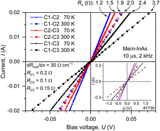
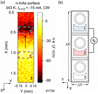
Measurements of I–V characteristics at 77 and 300 K revealed no deviation from Ohm's law; substrate resistance at RT progressively increased with the inter-contact distance as dRsub300K/dx = 3 Ω mm−1, amounting to Rsub = 1.7 Ω to Rsub = 3.4 Ω for the C1–C2 (C2–C3) and C1–C3 connections, respectively (see Fig. 3). Contact resistances were 10-fold smaller than the Rs and consisted of RC1 = 0.2 Ω, RC2 = 0.1 Ω and RC3 = 0.15 Ω (contact resistances normalized to the unit area are 7.2 × 10⁻⁵, 3.6 × 10⁻⁵ and 5.4 × 10⁻⁵ Ω cm2, respectively).Shown in Fig. 4a is a ΔX by ΔY false IR image of the troika at IC1C2 = −15 mA, that is, the 2D distribution of ΔL(x, y) = L(x, y) − L0(x, y), where L(x, y) is the radiation intensity of the activated troika, L0(x, y) is the intensity without a bias and XY is the plane parallel to the (100) plane. As a rule, IR images contain bright areas at the edges of the sample where the radiation exhibits an enhanced extraction efficiency due to edge effects and shape imperfections. We will ignore these edge effects, and, thus, further considerations will deal with the emission from the n-InAs substrate surface only, so the areas of interest will not include the sample edges, as shown in Fig. 4b by the dashed rectangle with an area of ΔXΔY.
As seen in Fig. 4a, the 2D radiation distribution is far from uniform; the IR map clearly indicates two distinguishable areas of low and high brightness above the C1 and C2 contact areas (see dashed small rectangles #1 and #2 in Fig. 4a). Very similar features to those shown in Fig. 4a were obtained for the chip activation using the contact combinations C2–C3 and C1–C3 pairs.
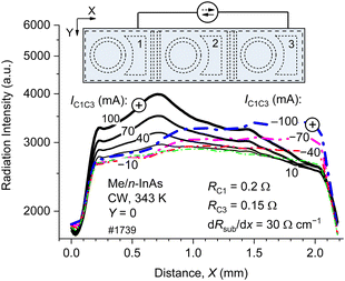
Shown in Fig. 5 is the IR radiation intensity distribution along the long side of the chip activated though the C1–C3 pair of contacts (raw data). The above distribution clearly reveals the heat dissipation bottlenecks, namely, two intensity steps at thin substrate regions located at x ∼ 0.6 mm and x ∼ 1.2 mm in Fig. 5. This result is not a surprise since these distribution steps naturally originate from the low lateral thermal conductivity in the regions of deep separation grooves. The surprise is that, at both polarities, the radiation peaked at the contact with the positive polarity and subsided at the negatively biased electrode (contact).
The difference in the Joule heat power dissipated at the two contacts with different resistance (RC1 = 0.2 Ω, RC3 = 0.15 Ω) could hardly be responsible for the lack of symmetry in the 1D distributions shown in Fig. 5, as the thermal generation is insensitive to the bias polarity. Moreover, the intensity behavior at a negatively biased contact at some contact pair connections contradicts the Joule heating law: the thermal emission intensity declines as the current increases. This contact feature, that is, the heat pump ability, is demonstrated in Fig. 6, where the maximum temperature rise with respect to ambient temperature value at a contact region is plotted against the current. As seen from Fig. 6, some regions above the contact appeared 1 K colder than the ambient temperature at a pumping current of ≈−50 mA. This means that, under these conditions, the Joule heat power is smaller than the heat pump power and the Peltier process dominates.
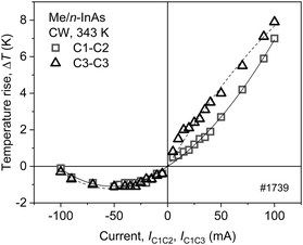 | ||
| Fig. 6 Maximum temperature rise ΔT in the contact regions C1 (X = 0.35–0.5 mm) in the contact pair C1–C2 (squares) and C3 in the pair C1–C3 (X = 1.6–1.75 mm) vs. current. | ||
The Seebeck effect, which is a mirror-like image of the Peltier process, has been observed using a noncontact IR sensing technique as described elsewhere.21 In our study, a temperature gradient was formed by a 0.98 μm diode laser emission (P = 0.1 W, τ = 0.5 s) with a ∼800 μm wide spot on the n-InAs substrate near one of the three mesa areas (Ai,j = 1, 2, 3). For example, a temperature difference of ΔTA1A3 = TA1 − TA3 = 313–315 = −2 K resulted in Seebeck voltage on the C1–C3 pair of contacts with a corresponding short circuit current of IC1C3 = −280 μA, while an alternative laser beam position (ΔTA1A3 = 314.5–313 = 1.5 K conditions) resulted in a sign change of the current induced by the Seebeck effect (IC1C3 = 280 μA).
The cooling ability of the Me/n-InAs junction could be also traced through an analysis of total radiation intensity measurements, presented in Fig. 7. The normalized total thermal emission intensity rise ΔLtot/area shown in Fig. 7 is understood as ΔLtot= Ltot(U ≠ 0) − Ltot(U = 0) = ∫ΔL(x, y) dx dy normalized to the integration area and refers to 1) the area above the whole n-InAs substrate surface (ΔXΔY in Fig. 4b) and 2) the areas designated by the dashed rectangles in Fig. 4a, that is, to the areas above the contacts. As seen in Fig. 7, at currents of (−20 ÷ 0) mA, negligible heating is observed in the area above the positively biased contact C2. At the same time, a temperature reduction is seen at the negatively biased contact C1 area, since the corresponding intensity integral is less than zero. The cooling ability of the C1 contact area remains down to ∼−100 mA, evidence both for the cooling ability saturation and the Joule heating enhancement. Note that at I = (−50 ÷ 0) mA, the integral thermal intensity is less than the ambient intensity, which means the sample surface is cooling as a whole.
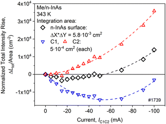 | ||
| Fig. 7 Normalized total intensity rise vs. the current IC1C2 at three integration areas: above the contacts C1 and C2 (triangles) and above the (100) n-InAs surface (clubs). | ||
Discussion
At 343 K, InAs attains a nearly intrinsic conductivity which is essential for the start of at least two current induced effects: heat transfer by the current17 and charge carrier exclusion.22 In an n-type semiconductor, the conduction band bottom is above the Fermi level by a value of En. The average energy of carriers in the conduction band is assumed to be 2kT for the phonon scattering mechanism. Therefore, the energy (En + 2kT) is taken from the lattice at the transition of an electron from the metal to the conduction band of the nondegenerate n-type semiconductor.17 On the other hand, the reduction of the charge carrier concentration initiated by the exclusion in InAs is also followed by thermal emission suppression and is accompanied by negative luminescence.23 The latter process is responsible for the sample temperature decay as well.13,14The abovementioned effects may be responsible for the sample cooling in our experiments as these particular effects are usually accompanied by other sample properties, namely specific features of I–V characteristics. As seen in Fig. 3, there are no grounds to consider any kind of barriers at the Me/n-InAs interface as the I–V characteristics are linear.
The electron–phonon drag is closely related to the cooling effect explanation as it is a bulk effect that does not prove the existence of interface barriers.24 However, in our case, the process is inverted so that it should be considered a phonon–electron drag process.
It is worth mentioning that the heat pump power of the Me/n-InAs structure in terms of the local temperature decrease ΔT ≈ 1 K appeared comparable with those reported for electronic pump engines other than Peltier coolers.25
The spatial nonequilibrium temperature distribution was smooth, and the cooling area covered the neighboring p–n junctions as well. Thus, the activation of current in the substrate (bias onto a Ci–Cj contact pair) could be useful in precise photometric measurements for temperature stabilization of a diode operating in photovoltaic mode (e.g., using the Ci–Ai pair of contacts).
Conclusions
The measurements of temperature in current activated Me/n-InAs structures revealed cooling of the sample near the contact that delivers electrons into n-InAs and heating of the opposite contact area. The surface temperature drop was as high as ΔT ≈ 1 K at an ambient temperature of 343 K and a CW current of I = 50 mA in spite of Joule heating. At currents higher than 50 mA, the above heat pump ability saturates. The results show a potential for the fabrication of heterostructures with a built-in cooler that is monolithically integrated with another electronic device, e.g., an LED or photodiode.Author contributions
N. D. Il'inskaya: resources, writing – Review & Editing (equal), S. A. Karandashev: methodology, validation, writing – review & editing (equal), T. S. Lukhmyrina: data curation, formal analysis (equal), visualization, writing – review & editing (equal), B. A. Matveev: conceptualization, formal analysis (equal), writing/original draft preparation, M. A. Remennyi: project administration, supervision, writing – review & editing (equal), A. E. Chernyakov: investigation, software.Conflicts of interest
There are no conflicts to declare.Acknowledgements
The authors wish to thank Gavrilov G. A., Kapralov A. A., Sotnikova G. Yu, Usikova A. A. (all from Ioffe Institute), Zakgeim A. L. (Submicron Heterostructures for Microelectronics, Research & Engineering Center RAS) as well as the personnel of LLC Ioffe LED Ltd. for their valuable contribution. The IR radiation intensity maps have been measured at the Center of Multi-User Facilities “Element Base of Microwave Photonics and Nanoelectronics: Technology, Diagnostics, and Metrology”.References
- S. A. Karandashev, T. S. Lukhmyrina, B. A. Matveev, M. A. Remennyi and A. A. Usikova, Phys. Status Solidi A, 2022, 219, 2100456 CrossRef CAS.
- M. Sieger and B. Mizaikoff, Anal. Chem., 2016, 88(11), 5562–5573 CrossRef CAS PubMed.
- T. Correia and Q. Zhang, New Generation of Coolers, 2014, vol. 34, p. 253 Search PubMed.
- L. Zhang, P. Han, K. Jin, L. Liao, C. Hu and H. Lu, J. Phys. D: Appl. Phys., 2009, 42, 125109 CrossRef.
- J. Oksanen and J. Tulkki, J. Appl. Phys., 2010, 107, 093106 CrossRef.
- G. Min and D. Rowe, IET Sci., Meas. Technol., 2007, 1, 329–332 CrossRef.
- X. Liu and Z. M. Zhang, Nano Energy, 2016, 26, 353–359 CrossRef CAS.
- J. Piprek and Z.-M. Li, Opt. Quantum Electron., 2016, 48, 472 CrossRef.
- C. T. Elliott, Philos. Transact. A Math. Phys. Eng. Sci., 2001, 359, 567–579 CrossRef CAS.
- V. I. Ivanov-Omskii and B. A. Matveev, Semiconductors, 2007, 41, 247–258 CrossRef CAS.
- P. Berdahl, J. Appl. Phys., 1988, 63, 5846–5858 CrossRef CAS.
- P. Berdahl, J. Appl. Phys., 1985, 58, 1369–1374 CrossRef CAS.
- V. I. Pipa and A. I. Liptuga, J. Appl. Phys., 2002, 92, 5053–5059 CrossRef CAS.
- L. Zhu, A. Fiorino, D. Thompson, R. Mittapally, E. Meyhofer and P. Reddy, Nature, 2019, 566, 239–244 CrossRef CAS PubMed.
- Y. Zhao, M. J. Jurkovic and W. I. Wang, J. Electrochem. Soc., 1997, 144, 1067 CrossRef CAS.
- A. L. Zakgeim, S. A. Karandashev, A. A. Klimov, R. E. Kunkov, T. S. Lukhmyrina, B. A. Matveev, M. A. Remennyi, A. A. Usikova and A. E. Chernyakov, Semiconductors, 2023, 57, 39–49 CrossRef.
- V. I. Stafeev, Semiconductors, 2009, 43, 1280–1287 CrossRef CAS.
- N. A. Sanjarovskii, I. B. Parfenteva, T. G. Yugova and S. N. Knyazev, Crystallogr. Rep., 2022, 67, 1095–1098 CrossRef CAS.
- V. M. Bazovkin, I. V. Mzhel'skii, G. L. Kuryshev and V. G. Polovinkin, Optoelectronics, Instrumentation and Data Processing, 2011, vol. 47, pp. 498–502 Search PubMed.
- T. S. Lukhmyrina, A. A. Klimov, R. E. Kunkov, N. M. Lebedeva, B. A. Matveev and A. E. Chernyakov, St. Petersburg State Polytechnical University Journal. Physics and Mathematics, 2023, 16, 119–125 Search PubMed.
- G. Y. Sotnikova, S. E. Aleksandrov and G. A. Gavrilov, in Optical Sensors 2011; and Photonic Crystal Fibers V, SPIE, 2011, vol. 8073, pp. 268–276 Search PubMed.
- D. A. Aronov, P. I. Knigin, Y. S. Korolev and V. V. Rubinov, Phys. Status Solidi A, 1984, 81, 11–45 CrossRef CAS.
- S. S. Bolgov, V. K. Malyutenko and A. P. Savchenko, Semiconductors, 1997, 31, 444–445 CrossRef.
- H. P. R. Frederikse, Phys. Rev., 1953, 92, 248 CrossRef CAS.
- X. Chen, V. V. Shvartsman, D. C. Lupascu and Q. Zhang, J. Appl. Phys., 2022, 132, 240901 CrossRef CAS.
| This journal is © The Royal Society of Chemistry 2024 |

