DOI:
10.1039/D3MA00696D
(Paper)
Mater. Adv., 2024,
5, 293-305
A highly sensitive and room temperature ethanol gas sensor based on spray deposited Sb doped SnO2 thin films†
Received
12th September 2023
, Accepted 17th November 2023
First published on 6th December 2023
Abstract
A room temperature ethanol gas sensor designed using antimony (Sb)-doped tin dioxide (SnO2, ATO) nanostructure thin films was prepared via the chemical spray pyrolysis method as a function of Sb concentration (0, 2, 4, 6, and 8 wt%) at 420 °C. Structural, surface, optical, electrical, and temperature-dependent resistance studies were carried out using XRD, FESEM, UV-visible, and four-probe electrical resistivity techniques. Structural and surface microstructure analysis of the films confirms the nanostructure formation. Optical band gap and electrical resistivity studies demonstrate that the n-type conducting behavior of the films increased upon Sb doping. Temperature-dependent sheet resistance analysis confirms that ATO thin films exhibit maximum resistance stability up to 350 °C. The sensitivity of the fabricated ATO sensors strongly depends on the surface structure of the films, and the adsorbed gas molecules cause a change in the resistance of the films. A significant improvement was observed in the recovery and response times of the sensors as a function of Sb-doping content and ethanol exposure level. The maximum ethanol response achieved in the 6 wt% Sb-doped SnO2 (ATO6) film was 842% for 50 ppm with a response and recovery time of 259/214 s, respectively. Hence, the ATO6 film exhibited a better sensing performance towards ethanol sensing applications.
1. Introduction
Detecting volatile organic compounds (VOCs) is very important for environmental monitoring, personal care, and the safety of factories.1 In particular, toxic gases such as carbon monoxide (CO), chlorofluorocarbons (CFCs), volatile organic compounds (VOCs), and sulfur pollute the atmosphere.2 In addition, VOCs in the atmosphere interact with greenhouse gases to form toxic molecules, and some of the VOCs, such as benzene, ethanol, acetone, and toluene, are dangerous to human health.3 Highly concentrated ethanol is extremely flammable and exhibits high toxicity, which can affect human health. The World Health Organization (WHO) has been monitoring the global and regional comparability of data concerning alcohol use and the consequences of alcohol consumption to study and improve risk assessment techniques.4 Additionally, VOCs also have significant use in biomedical research. In particular, bioethanol is a perfect alternative for replacing gasoline in the future, as reported by Yusoff et al.5 Furthermore, the detection of ethanol plays a crucial role in the food industry and traffic safety. Therefore, developing a suitable ethanol sensor is necessary for environmental monitoring. Several gas sensors that detect various VOC gases have been reported, such as metal oxide, metallic, and electrochemical gas sensors.6,7 Binary metal oxide semiconductors, such as undoped and donor/acceptor-doped SnO2, TiO2, In2O3, MoO3, and ZnO, have been widely explored as efficient gas sensors.8–12 Binary metal oxides possess excellent sensing properties and good thermal and chemical stability, and easy to deposit by a low-cost fabrication process. However, they require high operating temperatures, show poor selectivity, and consume more input power than composite and organic materials.13 Reducing the operating temperature of metal oxide gas sensors has become an exciting challenge for researchers.13 Developing a reliable gas sensor with excellent sensitivity and selectivity is challenging process. Importantly, designing room temperature gas sensors is an exciting challenge for researchers.
Doped SnO2 materials have been extensively studied for gas sensing applications owing to their excellent sensing behavior, low-cost production, thermal stability, and other excellent optoelectronic properties.14 Soheila et al. reported the Sb-doped SnO2 thin film for an enhanced gas sensing performance toward NH3 gas compared to acetone, ethanol, H2S gases at 100 °C for 50 ppm.15 Nanostructured SnO2 materials, such as nanopores,16 nano-hierarchical structures,17 nanorods,18 and nanofibers,19 exhibit better-sensing properties than bulk SnO2. Donor/acceptor-doped SnO2-based gas sensors have been fabricated using several techniques, such as sputtering, chemical vapor deposition, spin coating, and spray pyrolysis.20–22 Very few SnO2-based sensors studied have shown higher sensitivity towards ethanol at an optimum operating temperature higher than 200 °C.23 Biswas et al. theoretically analyzed the sensing mechanism of ethanol at 30 °C using SnO2 nano-columns.24 Shao et al. reported that highly ordered nanoporous Sb-doped SnO2 films showed enhanced ethanol sensing properties at operating temperatures as low as 100 °C.25 According to Yinglin et al., the sensitivity of SnO2 with an annulus-like nanostructure towards 100 ppm of ethanol increased to 17.3 at an operating temperature of 225 °C.26 However, high operation temperatures, short sensor life of the device, and power consumption are some of the issues that still need to be addressed for achieving a highly efficient gas sensor device.
In this report, nanostructured pure SnO2 (TO) and Sb-doped SnO2 (ATO) thin films were investigated for room-temperature ethanol gas sensor applications. ATO films were prepared with different concentrations of Sb using a facile spray pyrolysis process on a glass substrate at 420 °C. The film's crystalline, surface, and optical transmittance, electrical transport, and temperature-dependent electrical analyses were carried out as a function of Sb content. The gas sensing mechanism of the ATO films was examined at different ethanol gas concentrations at room temperature (30 °C).
2. Experimental method and characterization
2.1. Spray coating of TO and ATO thin films
Tin chloride dihydrate (SnCl2·H2O) and antimony pentachloride (SbCl5) were purchased from Sigma-Aldrich. Isopropyl alcohol (IPA), ethylene glycol (Eg), acetone, and concentrated hydrochloric acid (HCl) were purchased from Finar. All the substances and solvents were used in the as-received conditions without any purification. The precursor solution for the undoped SnO2 and Sb-doped ATO thin films was prepared using the following procedure: 0.2 M SnCl2·2H2O salt with the desirable quantity as a function of donor element was liquified in 10 ml of deionized water. Similarly, 0.2 M of SbCl5 salt with various (0, 2, 4, 6, and 8 wt%) concentrations was dissolved in 10 ml of IPA, and both solutions were separately stirred for 30 min. The Sn and Sb-based solutions were mixed, and 40 ml of ethylene glycol was added as a stabilizing agent. Furthermore, 2 drops of concentrated HCl were slowly added to make a transparent solution. Finally, the solution mixture was stirred to a homogeneous solution for 12 h at 30 °C.
TO and ATO thin films were coated on a glass substrate (dimensions: 7.5 × 2.5 cm2, purchased from ThermoFisher Scientific) with a maximum softening temperature of 450 °C. The substrates were cleaned using a standard procedure. The thin films were prepared dynamically using HOLMARC spray coating equipment (model HO-TH-04A). All the films were deposited at 420 °C. The substrate-to-nozzle distance was 18 cm, the spray duration was 60 s, and the output pressure was maintained at 2 bar for all the films. A total of 10 sprays were performed using 50 ml of the precursor solution. The undoped SnO2 and 2, 4, 6, and 8 wt% of Sb-doped SnO2 samples were labelled as TO, ATO2, ATO4, ATO6, and ATO8, respectively.
2.2. Characterization
The crystalline properties of the as-deposited SnO2 thin films were evaluated using an X-ray diffractometer (grazing incidence X-ray diffraction (GIXRD)) with Cu-Kα1 radiation (1.5406 Å); data were acquired at 30 min with a step size of 0.02. The Rietveld refinement technique was used to refine the XRD patterns using FullProf software. The surface morphology and homogeneity of the thin films were analyzed using field-emission scanning electron microscopy (FESEM; Carl Zeiss Supra 40 VP). Energy-dispersive X-ray spectroscopy (EDS; Oxford Xplore EDS model: CX-200) was used to study the elemental compositions of the films. Measurements of thickness and roughness were conducted using a stylus profiler (Model-KLA Alpha-Step-D-600). The films’ surface topography and surface roughness were characterized by atomic force microscopy (AFM; ANTON PARR) with a probe radius >10 nm and a scan range of 1 × 1 μm2. The optical transmittance spectra of the films were obtained using a UV-Vis spectrometer (PerkinElmer, Lambda 950). To characterize the surface charge state and binding energy of the as-deposited films, X-ray photoelectron spectroscopy (XPS; SPECS) was used. An Agilent B1500A instrument (HEM 150) was used to study the electrical transport properties. The thermal stability measurements were carried out using an in-house designed collinear four-probe technique.
2.3. Gas-sensing measurement
The ethanol gas sensing performance of TO and ATO thin films was tested using an in-house-developed gas sensor unit. A pictorial diagram of the in-house-developed gas sensor setup is shown in Fig. S1 (ESI†). The gas sensor setup consists of two mass flow controllers, ethanol as a testing gas (99.99% purity), dry air as a carrier gas (99.99% purity), system controlling units, a DC-power source (max: 30 V), Keithley's meter (model: 2010), a temperature controller, and a rotary pump. The ethanol flow rate was controlled using a mass flow controller. Furthermore, the vaporized ethanol concentration was measured in ppm using the following relationship (1),| | 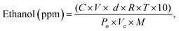 | (1) |
where C is the liquid ethanol (wt%) concentration, V is the volume of the liquid injected (μl), d is the density of ethanol (g ml−1), R is the universal gas constant (L atm K−1 mol−1), T is the absolute temperature (K), M is the ethanol molecular weight (g mol−1), Po is the chamber pressure (atm), and Vc is the volume of the chamber (L). A thin layer (150–180 nm) of an Au electrode was sputter-deposited onto the TO and ATO films to perform the sensing measurements. The TO and ATO film-based sensors were designed to check the sensitivity at different ethanol gas concentrations at 30 °C. When the ATO thin films were exposed to ethanol gas, the change in the resistivity of the films was measured using a four-probe setup. Gold (Au) contacts were used to provide metal-to-semiconductor contact. The sensitivity of the device was measured using S = (Rg − Ra)/Ra × 100, where Rg and Ra are the resistances of the films in the presence of ethanol and air, respectively.20 Typically, the sensor response time (τ90) represents the time required for a gas to go from zero to a specific resistance value and stabilize about 90% of the final value during the target gas exposure. The recovery time, the time required to acquire 10% of the initial resistance value (τ10), is calculated in the absence of a target gas and in the presence of air.27
3. Results and discussion
3.1. Crystalline analysis of the ATO films
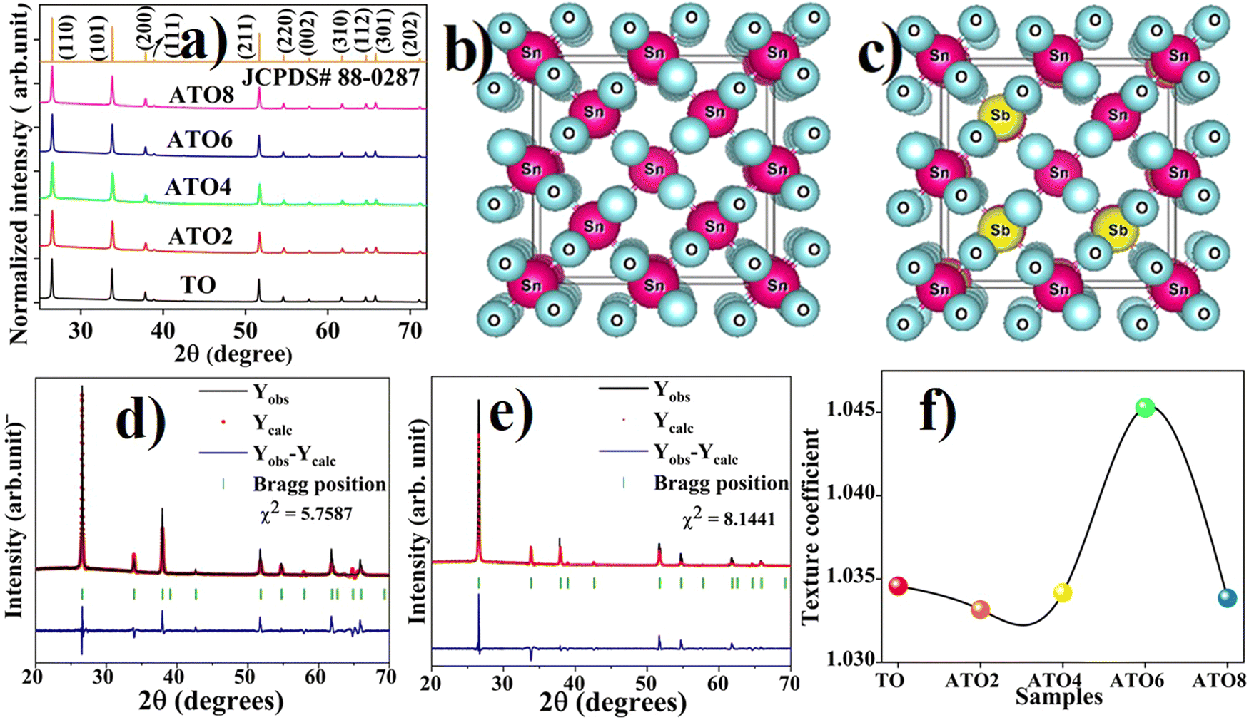
Fig. 1(a) shows the XRD pattern of TO and ATO thin films exhibiting a polycrystalline structure with a tetragonal crystal structure (JCPDS: 41-1445, P42/mnm space group).28 The crystalline structure of pristine and Sb-doped SnO2 systems is shown in Fig. 1(b) and (c). No secondary phase is observed upon Sb substitution into the Sn site of the SnO2 lattice. Moreover, the phase pure crystalline structure of the films confirms that at least 8 wt% of the Sb doping content can occupy the SnO2 lattice without changes in the crystal structure. The absence of Sb-related peaks in the XRD pattern suggests that Sb ions are successfully doped into SnO2 lattices. The Sb substitution also causes a small variation in the peak position toward a higher angle indicating a change in the lattice parameters,8 which causes a change in the interplanar distance values (d).8 The Rietveld refinement was employed to determine the lattice parameters by fitting the XRD pattern to all the films. The refined pattern of the pristine TO and ATO6 thin films is displayed in Fig. 1(d) and (e). TO and ATO thin film Rietveld refinement data exhibited a significant variation in the XRD pattern compared to the standard bulk SnO2 XRD pattern, indicating the thin film nature (Table 1). Also, upon increasing Sb doping from 2 to 6 wt%, the full-width at half-maximum (FWHM) of the diffraction peaks decreases. Beyond this concentration range, the FWHM increases, indicating peak broadening. A variation in d values results in a variation in the crystallite size. Based on the Rietveld refinement approach, lattice parameters of TO and ATO thin films have been calculated and are presented in Table 1. The average crystallite size (D) of the films was estimated using the Scherrer equation expressed as follows:15| |  | (2) |
where θ is the diffraction angle, and β is the full width at half maximum (FWHM). The estimated L values and standard deviations are presented in Table 1. These estimated average crystallite size values well-matched with the reported values.29 The crystallite size of ATO films decreases with an increase in the Sb doping concentration up to 6 wt%; beyond this concentration, the crystallite size slightly increases due to an increase in the lattice defects.
 |
| | Fig. 1 (a) XRD patterns of TO and ATO films and the standard XRD pattern of SnO2. (b) and (c) Crystal structures of undoped and Sb-doped SnO2 systems. Rietveld refinement XRD patterns of (d) TO and (e) ATO6 films. (f) Texture coefficient (TChkl) of the TO and ATO thin films. | |
Table 1 Structural, surface, optical, and electrical resistivity of TO and ATO thin films as a function of substrate temperature and Sb doping concentration
| Parameters |
TO |
ATO2 |
ATO4 |
ATO6 |
ATO8 |
| Lattices (a = b Å) |
4.742 |
4.735 |
4.721 |
4.718 |
4.739 |
| Lattice (c Å) |
3.181 |
3.175 |
3.163 |
3.151 |
3.176 |
|
D (nm) |
50.6 |
44.3 |
42.6 |
36.5 |
43.9 |
| STD (σ) |
19.4 |
33.1 |
40.6 |
62.3 |
69.5 |
| Thickness (nm) |
216 |
224 |
235 |
242 |
256 |
| Roughness (nm) |
16 |
19 |
21 |
24 |
27 |
| Tr. @ (550 nm %) |
79.7 |
92.4 |
93.3 |
93.6 |
86.1 |
|
E
g (eV) |
3.68 |
3.75 |
3.81 |
3.91 |
3.78 |
|
R
s (Ω sqr−1) |
4354 |
85.4 |
39.5 |
22.7 |
271.1 |
|
ρ (×10−4 Ω cm) |
940.6 |
19.41 |
9.274 |
5.51 |
69.45 |
The TO and ATO8 films show the highest crystallite size, an observation that is further supported by FE-SEM and AFM analysis. Significantly, the crystalline SnO2 phase changed into a polycrystalline phase because of the preferred orientation (texture coefficient) of the XRD peaks in a particular plane direction due to variation in grain growth. The TO and ATO thin films texture coefficient (TChkl) was estimated from all the peaks appearing in the XRD patterns using the Harris relationship.30 It is identified that all the films exhibited relatively higher (TChkl) values towards the (200) plane direction. A similar texture behavior was also observed for W-doped nanocrystalline tin oxide thin films.31 Hence, the ATO thin films have strong grain growth in the (200) plane direction. Also, it should be noted that there is a significant variation in TChkl values as a function of Sb doping concentration (Fig. 1(f)). Doping of 2 wt% Sb into the SnO2 lattice led to a decreased TChkl value due to the growth of several smaller grains in many directions during the nucleation process. Further, increasing the Sb doping concentration, the TChkl values increased up to for the ATO6 film and beyond that they decreased. An ATO6 film has a maximum TChkl value of 1.045 compared to other films, indicating strong nucleation and grain growth in this plane direction.31 The ATO8 film shows a decreasing TChkl value indicating the greater influence of structural defects in the film. Interestingly, the preferred orientation along a particular plane direction can effectively control the charge transport properties of the films.28 It is also reported that the Sb substitution in the SnO2 matrix leads to a variation in oxygen vacancy defects in the SnO2 system. Substitution of a high concentration of Sb into the SnO2 system may affect the transport properties due to the influence of oxygen vacancy defects on the mobility of the charge carrier.32
3.2. Surface morphology analysis of the TO and ATO films
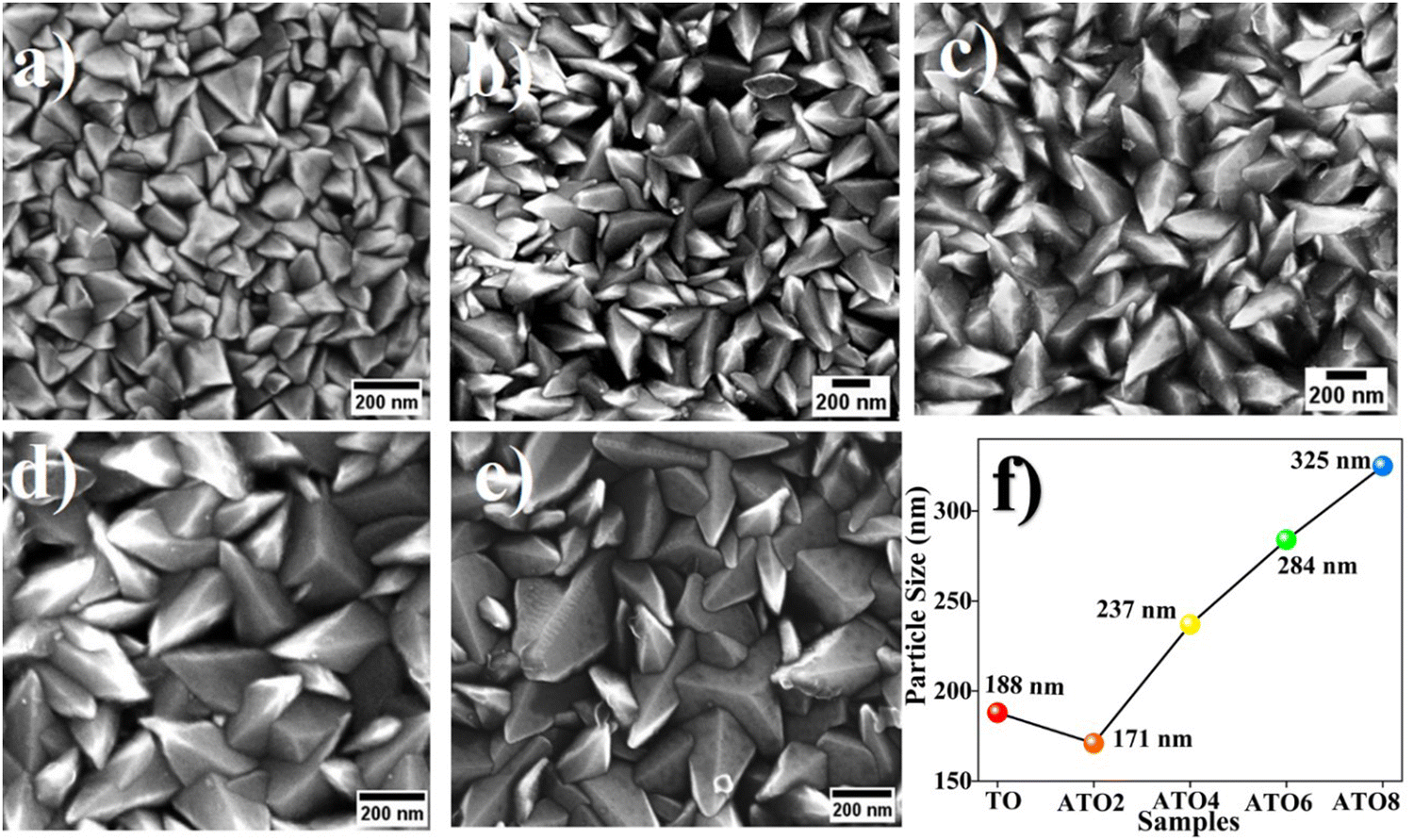
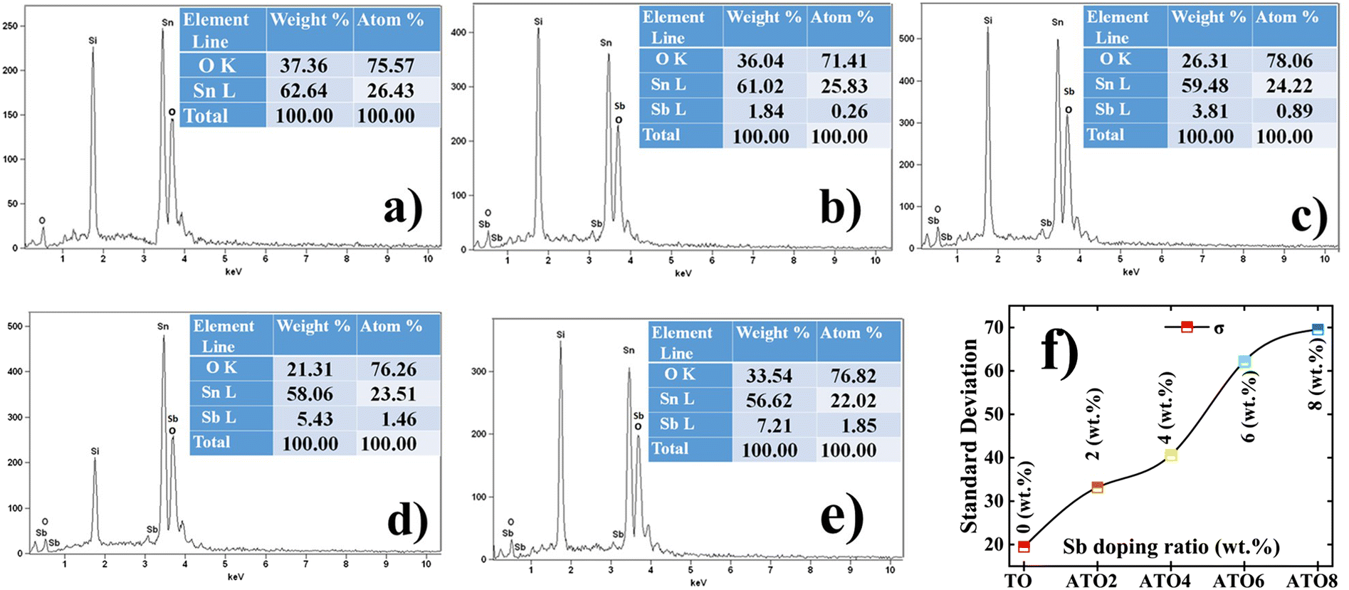
Fig. 2(a)–(e) depict the FE-SEM surface morphology images of the TO and ATO thin films. Polygon-shaped particle formation is observed in all the films.18,32 Substitution of Sb into the Sn site of the SnO2 lattice leads to a significant variation in the surface morphology of the films. The polygon-shaped particles are densely formed over the entire region, and this surface structure is consistent with previous reports.18,32 It is identified that the polygon-shaped particle size increased with increasing Sb-doping concentration. These results not consistent with crystallite size analysis. It is well known that the particles are formed, when more than one similarity oriented grains are combined. Also, the grain growth with strong texture behavior leads to more considerable particle formation when several similar direction grains are compared, as reported by Turgut et al.33 This result is consistent with the XRD analysis of the texture behavior of the film. The particle size of the films was estimated using ImageJ software. It is identified that the particle size increases from 188 nm for the TO film to 325 nm for the ATO8 film with an increase in the Sb concentration leading to enhanced grain growth (Fig. 2(f)). The film deposited at 6 wt% of the Sb (ATO6) dopant consists of relatively homogeneous and nearly uniform particles. The nanocrystalline ATO films are crack-free, which is essential for the sensor because a crack on the film surface may affect the sensitivity. Additionally, the nanostructure enhances the physisorption process, resulting in a better sensing performance of the films. The chemical composition of TO and ATO films was confirmed using EDS analysis, as shown in Fig. 3(a)–(e). The presence of host and donor elements, such as Sn, O, and Sb, is visibly identified from their peaks in the spectra; simultaneously, the Si peak originated from the glass substrate. Glass composition-related other peaks also appeared, but those peaks are unmarked. The elemental composition significantly varies as a function of the Sb doping concentration. A small deviation in the chemical composition was observed for all the films compared to the standard stoichiometric ratio of the SnO2 system.18,32 Slight deviations in the compositional balance of ATO films also resulted from slight variations in spray dynamics during aerosol spraying onto the substrate.
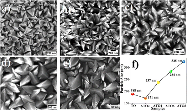 |
| | Fig. 2 FE-SEM surface morphology images of the (a) TO, (b) ATO2, (c) ATO4, (d) ATO6, and (e) ATO8 thin films. (f) ImageJ software estimated particle size from FE-SEM mages of the TO and ATO films. | |
 |
| | Fig. 3 EDS spectra of the Sn, O, and Sb elemental composition ratio of the films: (a) TO, (b) ATO2, (c) ATO4, (d) ATO6, and (e) ATO8 thin films. (f) The variation of the standard deviation with the Sb doping ratio of the TO and ATO films. | |
Hence, Sb substitution significantly impacts the SnO2 system by creating different defects, which can lead to a variation in the surface structural properties. To identify the nucleation and growth process as a function of the Sb-doping ratio of the SnO2 system, the standard deviation (σ) values were estimated using crystallographic data analysis followed by Babar et al.34 An estimated value of σ is shown in Fig. 3(f), and values are also given in Table 1. It is identified that the σ value of the TO film progressively increased with the Sb doping ratio. This confirms that the TO film has strong nucleation and growth in all directions. In contrast, ATO films have strong texture behavior due to the directional-dependent grain growth in a particular film direction, confirming a greater deviation from the TO film. This obtained result was consistent with the results of Turgut et al. showing increasing standard deviation values with increasing Mo doping concentration for SnO2 thin films.35 Importantly, this variation in standard deviation is strongly reflected in the surface features of the films, like increasing particle size and surface roughness.
3.3. Analysis of surface roughness
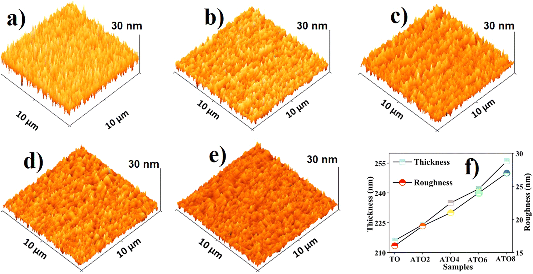
3D surface topography images of spray-deposited TO and ATO thin films are shown in Fig. 4(a)–(e). A granular structure of the film changes to a needle-like structure as the Sb concentration increases.36 The needle-like structure is formed by inhomogeneous grain growth in the perpendicular direction upon increasing Sb substitution. Generally, grain growth in the lateral direction increases the surface roughness, while grain growth in the normal direction (perpendicular to the plane) leads to uniform/dense film formation.37 The surface roughness of the granular film is relatively less than that of the needle-like film.38 The root mean square roughness (RMS) of the TO and ATO films determined from the AFM image results are compared with the stylus profiler instrument results. The RMS roughness increases with an increase in the Sb concentration, which substantially influences the sensing performance. The thickness of the film also plays a vital role in surface behavior, and the surface roughness of the thin film shows a significant influence on the surface charge transfer process.39 A Stylus profiler instrument was used to measure the thickness and roughness of the films and the estimated values are given in Table 1 and also shown in Fig. 4(f). The significant variation in the film thickness/roughness is due to the increasing Sb content. A film with high surface roughness significantly affects the sensing performance due to the low-level surface chemisorption of targeted gases.
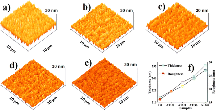 |
| | Fig. 4 3D AFM images of the (a) TO, (b) ATO2, (c) ATO4, (d) ATO6, and (e) ATO8 thin films. (f) The RMS roughness of the films depending on the Sb doping concentration. | |
3.4. Analysis of the optical properties
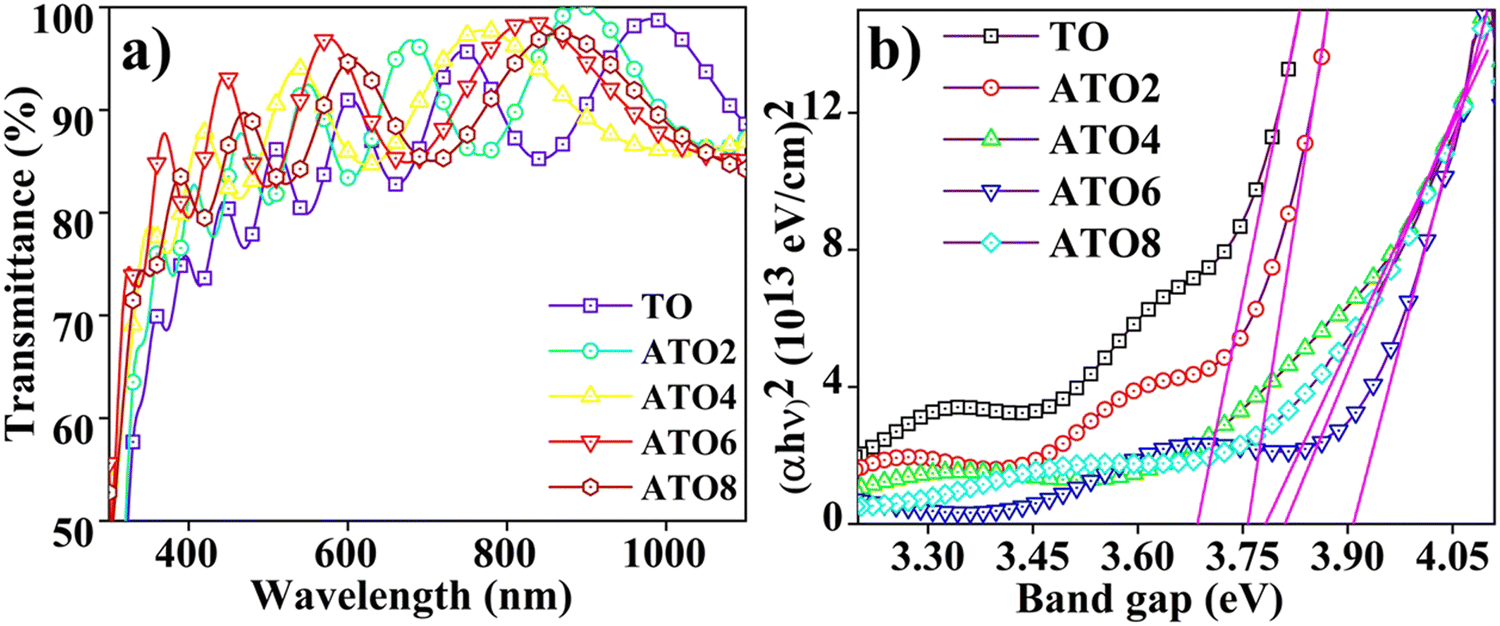
The TO and ATO thin films exhibited higher transmittance in the visible region (Fig. 5(a)), and all the ATO films showed an average transmittance of more than 85% (Table 1). The transmittance of the films improves with an increase in the doping concentration up to 6 wt% and then declines at a higher doping concentration owing to more elevated surface roughness and thickness.40 Film thickness also plays a vital role in transmittance properties, as increased film thickness can improve reflectance or scattering of light.32 Also, the absorption of free carriers by native oxygen vacancies contributes to decreased optical transmittance.41 The optical transmittance of ATO films in the near-infrared region (NIR) decreases because of the excess electron carrier concentration at the conduction band edge, facilitating carrier collision (Moss–Burstein effect).42 The Tauc relationship was used to estimate the TO and ATO films' optical band gap (Eg) values.43 The TO and ATO films' calculated direct bandgap values as a function of Sb concentration are provided in Fig. 5(b) and Table 1. The undoped SnO2 film shows a band gap value of 3.68 eV, which matches previously reported values.21,32 The Eg value increases as a function of the Sb content for up to 6 wt%, which indicates a Fermi level shift near the conduction band owing to an improvement in the free carrier at the bottom of the conduction band. The higher Sb concentration (8 wt%) bandgap value significantly decreased due to the concentration quenching effect near the NIR region,42 which can also significantly affect the free carrier mobility.44 In addition to this, the film roughness also influences the bandgap; an increase in the surface roughness can cause more light scattering, resulting in decreased transmittance.44 The transmittance decreases, eventually decreasing the band gap. Hence, this significant variation in the ATO film bandgap has a substantial role in the charge transfer process of the material.
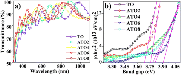 |
| | Fig. 5 (a) Transmittance spectra of TO and ATO films with different Sb contents and (b) Tauc plots of the films as a function of the Sb-doping content. | |
3.5. Electrical resistivity study
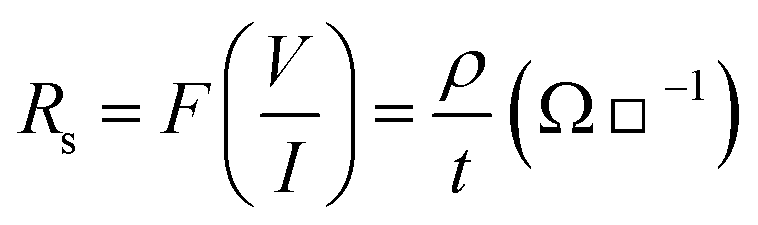
TO and ATO films' room temperature electrical resistivities were measured using a collinear four-point probe method. The sheet resistance (Rs) was estimated using the following relationship:45| |  | (3) |
where sheet resistance Rs is in Ω per square, F is the correction factor (4.532 for square), I is the applied current, V is the measured voltage drop, ρ is the film's resistivity, and t is the thickness of the films. The estimated values of the resistivity and sheet resistance of TO and ATO films are given in Table 1. The film's resistivity decreases up to the 6 wt% of the film (ATO6), indicating perfect substitution of Sb5+ in the Sn4+ site of the SnO2 lattice site. Upon further increasing the doping content (AT08), resistivity increases because of large free-carrier collisions, leading to decreased mobility.46 Hence, the ATO6 film shows a relatively better resistivity than the other deposited films.
3.6. Surface charge state analysis
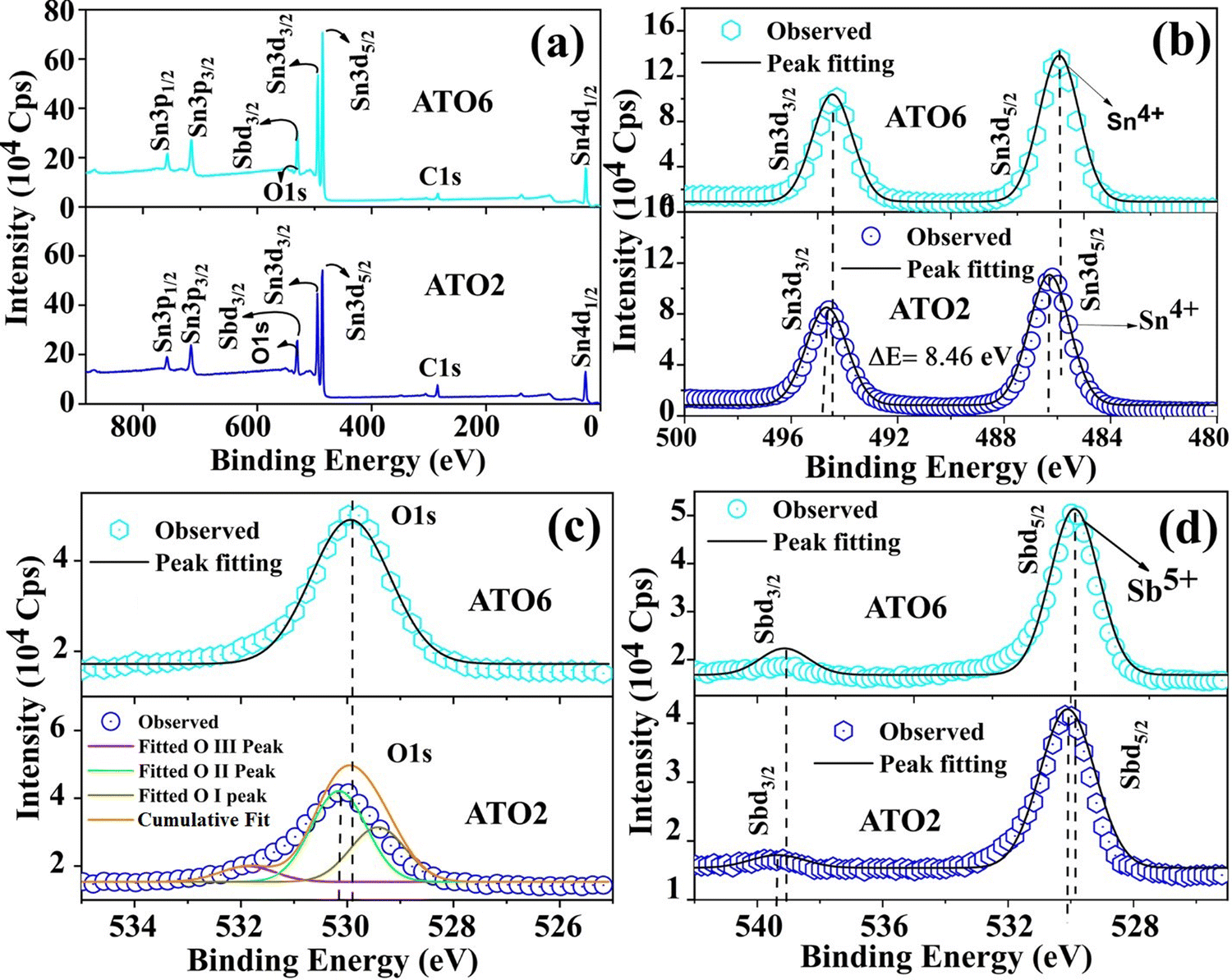
To understand the charge transport mechanism, the XPS measurement was carried out to identify the surface charge states of elements in the ATO thin films. Fig. 6(a) illustrates the survey scan spectra of the selected ATO2 and ATO6 thin films, indicating the presence of the constituent elements such as Sn, O, and Sb.34 The survey scan spectra showed a significant variation in peak intensity and a small peak position variation with Sb doping concentration. The survey spectra also exhibited a C1s peak at 285 eV, corresponding to surface contamination before exposure of the film to the ambient atmosphere.47 To determine the actual charge states of Sn3d, O1s, and Sb3d states, Gaussian peak fitting was performed. The narrow scan spectra with Sn3p3/2 and Sn3p5/2 peaks of the ATO2 and ATO6 thin films are shown in Fig. 6(b). The binding energy peaks observed at 485.8 eV and 494.3 eV confirm the Sn3p5/2 and Sn3p3/2 states, respectively, and the difference of 8.46 eV between these two binding energies confirms that Sn is in the 4+ charge state.34 A small peak shift is observed in the oxidation states of the ATO6 film compared to the ATO2 film.
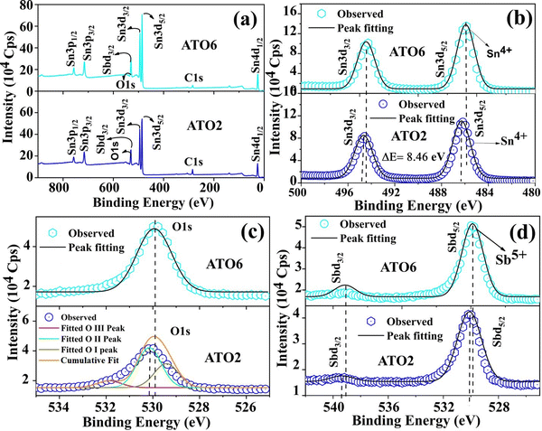 |
| | Fig. 6 The XPS full survey scan spectrum (a), Sn3d narrow scan spectrum (b), O1s narrow scan spectrum (c), and Sb3d narrow scan spectra (d) for ATO420 and ATO450 films. | |
Fig. 6(c) depicts the narrow scan spectra with O1s peaks centered at 530.1 eV for ATO2 and ATO6 thin films. To identify how the oxygen/oxygen-related defects influence the ATO films, the O1s spectrum was deconvoluted into three peaks. The oxidation state of the O 1s spectra deconvoluted for three peaks appear at 530.1 eV (O I), 531.2 eV (O II), and 532.3 eV (O III) binding energies states where indicated in the ATO2 film (Fig. 6(c)).34 The O I peak is due to the formation of oxygen with metal Sn ions (Sn–O bond); the OII peak is due to the oxygen deficiency in the SnO2 film. In contrast, the O III peak is generally attributed to the chemisorbed or dissociated oxygen or hydroxyl groups on the film's surface.47 The ATO6 film exhibited a slight variation in the O1 spectra compared to the ATO2 film. The narrow-scan spectra of Sb3p3/2 and Sb3p5/2 in Fig. 6(d) show binding energy peaks at 539.1 eV and 529.8 eV.34 The observed Sb binding energy values reveal that Sb exists in the Sb5+ charge state. The ATO6 film shows a lower binding energy shift than the ATO2 film. The lower binding energy of Sb5+ ions can effectively enhance the free charge carrier, improving ATO films' electrical transport properties. It has been reported that the perfect doping of Sb5+ into the SnO2 lattice site may increase the free carrier concentration and lead to higher mobility values.34,47
3.7. Thermal stability analysis
Thermal stability is one of the essential properties of metal oxide-based sensors. The thermal stability of TO and ATO films was estimated by measuring the temperature-dependent sheet resistance using the four-probe method. The experiment was carried out at 200 to 400 °C in intervals of 50 °C and different durations of 1, 2, 3, and 4 h. Fig. 7(a)–(e) illustrate the annealing time vs. sheet resistance plot of the TO and ATO films. All the films show different thermal stabilities at different annealing temperatures and durations. The TO, ATO2, and ATO8 films exhibit decreasing sheet resistance upon increasing the annealing temperature up to 300 °C, beyond which the sheet resistance increases. The sheet resistance values of ATO4 and ATO6 films decrease to 350 °C and grow with a further increase in the temperature. In addition, the sheet resistances of all the films increase with the increase in the annealing time (Fig. 7(f)). Also, the sheet resistance of all the films decreases with an increase in the annealing temperature up to 350 °C indicating the semiconducting nature of the films, which is helpful for gas sensing. In contrast, an increase in the sheet resistance with an increase in the annealing temperature and annealing duration indicates metallic-like behavior, adversely affecting the sensing performance.
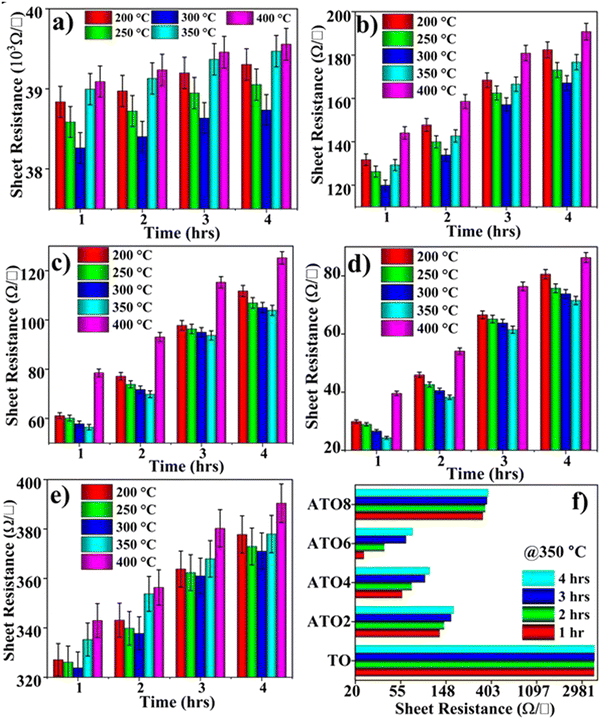 |
| | Fig. 7 Thermal stability studies of the (a) TO, (b) ATO2, (c) ATO4, (d) ATO6, and (e) ATO8 thin films at 200–400 °C with different annealing durations of 1, 2, 3, and 4 h. (f) Comparison of the sheet resistance of the films annealed for different durations at 350 °C. | |
Therefore, the initial decrease in the sheet resistance observed in all the TO and ATO films is ascribed to an increase in the carrier concentration and mobility supported by the thermally generated charge carriers. Films exhibiting metallic-like behavior at higher annealing temperatures show a rapid decline in the electrical properties, mainly attributed to the scattering of the charge carrier.48 At high temperatures, more thermally activated charge carriers can be generated, which undergo scattering and decrease carrier mobility.49 These experimental results reveal that ATO films possess good thermal stability for application as gas-sensing materials.
4. Ethanol gas sensing
4.1. Response study
The ethanol gas sensing performance was studied from 10 to 50 ppm (interval of 10 ppm) gas concentrations at 30 °C. Fig. 8(a) shows the response (S) curves of the TO and ATO film-based gas sensors. The reactions of pristine TO and ATO thin films were characterized based on transient sensing curves, and the determined values are given in Table 2 and in Table S1 in the ESI.† The response behavior of the TO film improves linearly with an increase in the ethanol gas concentration. A similar response behavior is observed for the ATO films. The response of the TO film ranges from 0.2 to 4.7% for 10 to 50 ppm of ethanol gas, respectively. However, the ATO thin films exhibit a relatively higher response than the TO film. Furthermore, the response behavior of ATO films improves upon increasing the Sb concentration up to 6 wt% (ATO6), beyond which the response decreases. The maximum response of 842% was achieved in the ATO6 film toward 50 ppm of ethanol gas concentration at 30 °C (Table 2). This value is relatively high compared to the NiO decorated SnO2 composite thin film-based ethanol gas sensor which exhibits a more heightened response value of 123.7 toward 1000 ppm ethanol at an operating temperature of 250 °C.50 The improved response of the ATO6 film is attributed to its enhanced charge transport behavior, which promotes surface charge carrier interactions with the adsorbed gas molecules. Several researchers also reported that a donor-doped SnO2 thin film exhibited enhanced gas sensing behavior compared to the pristine film due to its improved charge transport properties.2,6,8 Moreover, the appropriate Sb substitution into the Sn site of the SnO2 lattice leads to many surface free charge carriers.30 In contrast, TO and ATO8 films perform poorly when exposed to targeted gas concentrations due to their low charge transport properties.
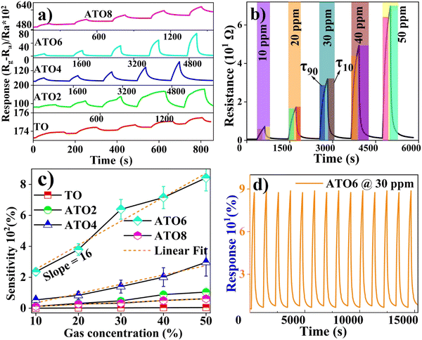 |
| | Fig. 8 (a) Gas sensing behavior of the TO and ATO films towards ethanol gas at 10–50 ppm. (b) Enlarged view of the sensing behavior of the ATO6 film. (c) Sensing plot. (d) Cyclic response study of an ATO6 film towards 50 ppm of ethanol. | |
Table 2 Ethanol gas sensing performance of TO and ATO thin films in comparison with other reported SnO2 system-based ethanol gas sensors
| Materials |
Deposition technique |
Working temperature (°C) |
Target gas (ppm) |
Response time (s) |
Recovery time (s) |
Response S (%) |
Ref. |
| 8 wt% Sb-doped SnO2 |
Spin-coating |
100 °C |
20 |
54 |
54 |
20.6 |
54
|
| 4 wt% Pd-doped SnO2 |
Spin-coating |
RT |
100 |
∼30 |
— |
3.36 |
55
|
| 3 wt% Pt-doped SnO2 |
Spin-coating |
400 |
200 |
∼25 |
— |
1.2 |
56
|
| 2.2 wt% Ce-doped SnO2 |
Co-sputtering |
225 |
100 |
4 |
45 |
5 |
20
|
| 3 wt% Er-doped SnO2 |
Coprecipitation |
240 |
100 |
45 |
40 |
48 |
57
|
| Pd/SnO2 |
Hydrothermal |
300 |
100 |
1.5 |
18 |
— |
58
|
| Fe2O3–SnO2 |
Spin-coating |
300 |
100 |
57.5 |
|
57.5 |
59
|
| TO |
Spray pyrolysis |
RT |
50 |
79 |
32 |
4.7 |
Present work |
| ATO2 |
Spray pyrolysis |
RT |
50 |
127 |
101 |
104 |
| ATO4 |
Spray pyrolysis |
RT |
50 |
205 |
263 |
296 |
| ATO6 |
Spray pyrolysis |
RT |
50 |
259 |
214 |
842 |
| ATO8 |
Spray pyrolysis |
RT |
50 |
86 |
179 |
61 |
The response results of all the films are compared with those of pure SnO2, doped SnO2, and composite materials based on the SnO2 system.8 The response study was conducted three times to confirm the reliability of the sensor, and the transient sensing curves show similar sensing behavior (Fig. S2, ESI†). The transient response times/recovery times of the pristine TO and ATO thin films were obtained from the transient response curves (Fig. 8(b)), and the values are presented in Table 2 and Table S1 (ESI†). The response time/recovery time of the TO and ATO films improved with an increase in the ethanol gas concentration. All the films' response time is higher than the recovery time. The TO thin film exhibited a relatively lower response/recovery time than ATO films due to poor interaction with target gas molecules. However, we inject the same level of targeted ethanol gas molecules but a low level of the gas molecules, only interacting with the TO film surface. This low-level gas molecule interaction leads to low response/recovery times and low gas sensing performance. The TO film exhibited a relatively lower surface roughness and poor surface charge transport behaviors. These could be the main reason for the low-level interaction of the gas molecules. A significant improvement is observed in the response and recovery time of the sensors as a function of the Sb doping process; notably, the ATO6 film shows a relatively better response and recovery time of 259 s and 214 s, respectively, toward 50 ppm of ethanol. The faster recovery time of the film indicates that the adsorption process of oxygen ions in the response process is slower than the desorption of oxygen ions from the air during the recovery process. To decrease the response time, the sensor surface needs to adsorb more ethanol molecules to reach the maximum value in a short time. The ATO thin film-based sensor is superior to previously reported sensors because of its low-level gas detection, fast response/and recovery time, and simple fabrication techniques.20 Vaishnav et al. reported that the maximum sensor response was achieved with 5 wt% of the Sb-doped SnO2 film at a working temperature of 400 °C.51 Li et al. concluded that the improved gas concentration within the experimental gas concentration limits enhanced the sensor response.52 The large variation in the surface nanostructure size generally affects the adsorption of gas molecules. The decreased sensitivity of the ATO8 film is due to large free-carrier collision at higher doping contents of Sb. Fig. 8(c) shows the response values of the TO and ATO films vs. ethanol gas concentration plots. The linear fit of each plot's slope exhibits the sensors' sensitivity. The TO film has very low sensitivity because of a low surface charge carrier interaction with adsorbed ethanol gas.32 In the case of ATO films, the sensitivity of ethanol gas improves as a function of Sb doping up to 6 wt% (ATO6) and decreases after that (Table S1, ESI†). Fig. 8(d) illustrates the cyclic response study of the ATO6 film exposed to a concentration of 50 ppm of ethanol gas at 30 °C. The ATO6 film with cycle response performance up to 15![[thin space (1/6-em)]](https://www.rsc.org/images/entities/char_2009.gif) 000 s for 14 cycles exhibits high cycling stability and a fast response/recovery time towards the targeted gas.
000 s for 14 cycles exhibits high cycling stability and a fast response/recovery time towards the targeted gas.
4.2. Sensing mechanism of the sensor
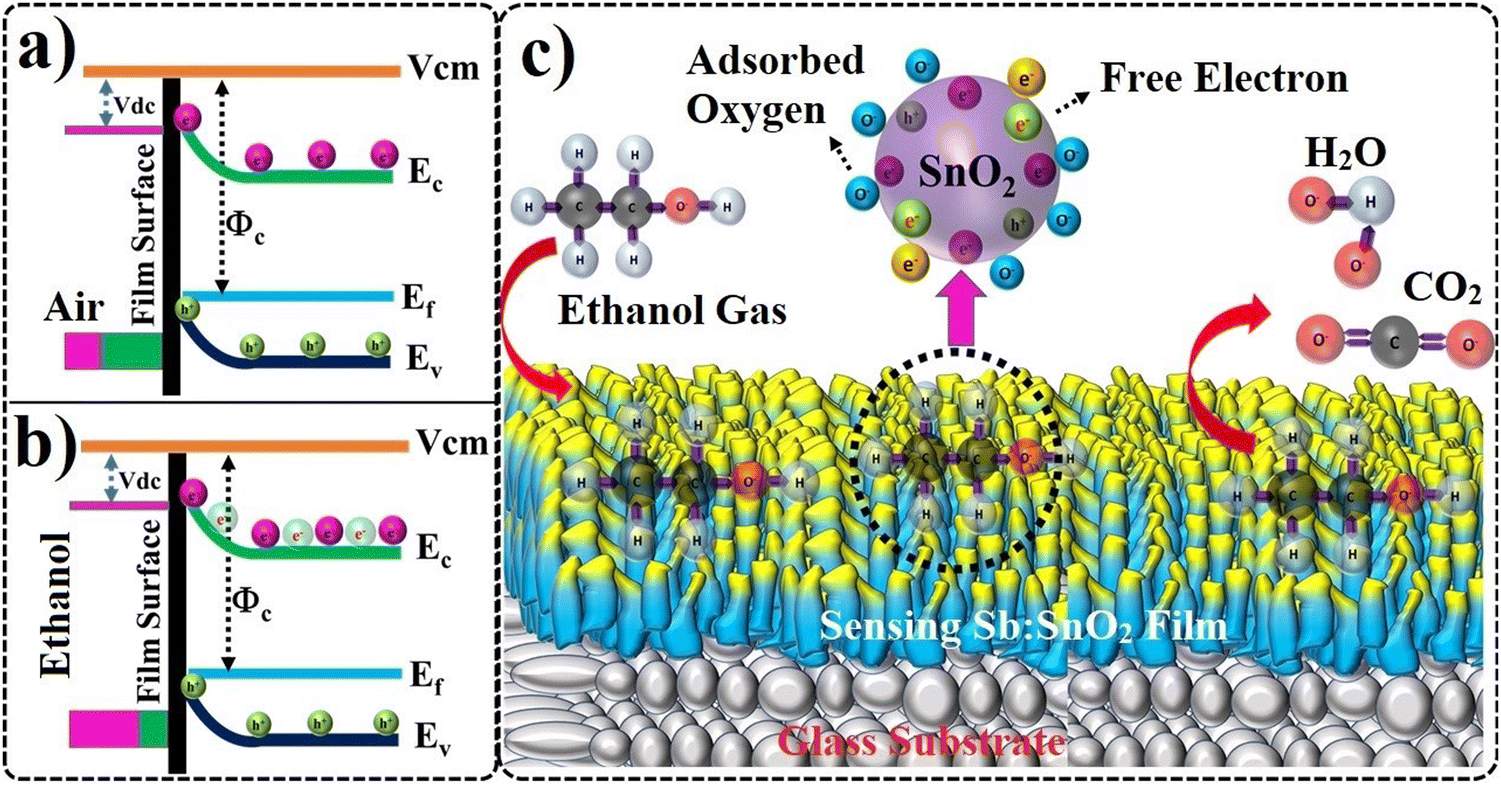
Significant changes in their electrical conductivity generally characterize gas molecules' interaction with metal oxide systems.32 Due to the adsorption process, dry air on the sample surface creates oxygen ions (2O−).52 A sample's electrical resistivity remains mostly the same when exposed to dry air. Furthermore, target gas exposed on the sample surface interacts with adsorbed oxygen ions to create a surface-conducting electron.32,53 The metal oxide's electrical resistance increased or decreased due to its type of semiconducting behavior. In the case of ethanol gas molecules, exposure to n-type materials significantly reduces the resistance. These adsorbed oxygen ions undergo desorption upon exposure to ethanol gas, even at room temperature.2,6,8 Also, the adsorption and desorption of ethanol gas on the sample surface led to a variation in the surface charge carrier concentration, leading to a change in the electrical resistivity of the sample.32Fig. 9(a) and (b) present the ATO film energy band diagram and charge transport processes in the presence of air (a) and ethanol (b). Fig. 9(c) shows a schematic of the sensing mechanism of the ATO film in the presence of ethanol. The free carrier offered by Sb ions leads to a decrease in the resistivity of the films. The low resistive behavior of the ATO film leads to a high surface charge carrier interaction with the targeted gas molecules. As a result, the free carrier interaction with gas molecules also changes the resistance more effectively in the ATO film. The exposure of ethanol gas leads to adsorbed oxygen ions, thus changing the carrier transport properties and increasing the resistance of the films. The film's resistance increases when oxygen ions are adsorbed on a film surface, and the gas molecules capture electrons.8 During the sensing process, ethanol was in contact with the film. After that, it decomposed into CO2 and H2O molecules. Furthermore, these CO2 and H2O gas molecules are removed during evacuation. The resistance value is returned to its original value when the gas is off. During the test, ethanol (target gas) and air (carrier gas) were switched ON/OFF based on their saturation point. The maximum and minimum gas response curves were obtained as a function of ethanol exposure time.
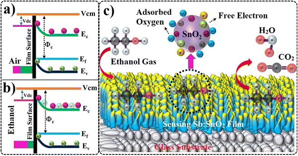 |
| | Fig. 9 Schematic of the energy band diagram along with charge transport processes in the presence of air (a) and ethanol (b). Schematic of the ethanol sensing mechanisms of ATO films (c). | |
4.3. Stability and selectivity tests
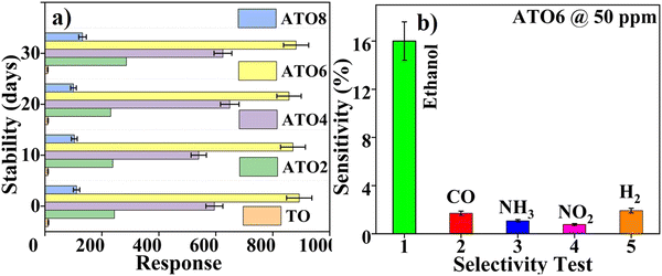
The applicability of TO and ATO thin films, as ethanol sensors, was tested using stability and selectivity studies. The stability test was performed by injecting 50 ppm of ethanol gas towards TO and ATO thin films every 10 days for 30 days to determine their sensing performance (Fig. 10(a)). The TO and ATO films show small variations in their response behaviors with increasing ageing times. In the presence of ethanol gas, the ATO films exhibit slow degradation, while the sensing behavior of ethanol gas is more prominent. We observed a slight decline in TO film sensing behavior upon ethanol gas injection. Moreover, the stability of the ATO films is improved with an increase in the Sb doping concentration up to 6 wt%, beyond which it decreases. Furthermore, selectivity analysis was performed to understand the sensing ability of the film towards ethanol in the presence of other gases. We also compared the sensing behavior of ethanol with that of CO, NH3, H2, and NO2 gases under similar operating conditions. Pristine TO and ATO thin films exhibit much variation in selectivity towards ethanol gas compared to other test gases at a concentration of 50 ppm (Fig. 10(b)). There was a relative increase in the selectivity of ATO films towards ethanol gas compared to other gases, as evidenced by the first response/recovery behavior (Fig. 9(b)). It was found that ATO6 films were more selective towards ethanol gas than CO/NH3/H2/NO2 gases. Free charge carriers facilitated using a doping process led to the high surface charge carrier interaction, which explains the stability and selectivity of the ATO6 film. In addition, the significant surface area interaction of the ATO6 film helps in adsorbing more ethanol, resulting in good selectivity/stability behaviors. Hence, the results demonstrate the excellent performance of ATO6 films for ethanol sensing applications compared with other deposited films.
 |
| | Fig. 10 (a) Stability study of TO and ATO films towards 50 ppm of ethanol gas at 30 °C. (b) Selectivity test of the TO and ATO films towards ethanol, CO, NH3, H2, and NO2 gases injected at 50 ppm at 30 °C. | |
5. Conclusions
Sb-doped SnO2 thin films with a highly dense nanostructure were prepared via the chemical spray pyrolysis method for room temperature ethanol gas sensing application. The impact of the Sb doping content on the structure, surface, optical, and thermal stability properties of SnO2 thin films was systematically investigated. The crystallite size of the films decreases with an increase in the Sb content up to the ATO6 film and beyond that it increases, and this leads to a significant variation in the surface charge transport properties. FE-SEM analysis indicates the formation of polygon-shaped nanostructured particles with dense film formation, which positively impacts the surface charge transport properties. The maximum resistance stability was achieved in the ATO6 thin film up to 350° at 4 h. The ATO films showed good sensing performance compared to the pristine SnO2 film due to their improved charge transport properties. The ATO6 film exhibited a maximum response of 842% and a response/recovery time of 259/214 s at 30 °C towards a concentration of 50 ppm of ethanol gas. The ATO6 film exhibited good selectivity for ethanol gas sensing at 50 ppm concentration compared to other CO, NH3, H2, and NO2 gases. Hence, the results obtained in this study indicate the applicability of the ATO film for ethanol sensing at room temperature.
Conflicts of interest
There are no conflicts to declare.
Acknowledgements
Dr Ramarajan R. thankfully acknowledges the UGC Government of India for the financial assistance (Dr D. S. Kothari Postdoctoral Fellowship Program: award letter number with data: F.4-2/2006(BSR)/PH/20-21/0152). All the authors acknowledge the Surface Engineering Division, CSIR-NAL, and the Department of Physics, IISc Bengaluru, for helping with the fabrication and testing of the gas sensor.
References
- X. Zhou, S. Lee, Z. Xu and J. Yoon, Chem. Rev., 2015, 115, 7944–8000 CrossRef CAS PubMed.
- Z. Merati and J. Basiri Parsa, Appl. Surf. Sci., 2018, 435, 535–542 CrossRef CAS.
- S. Weichenthal, R. Kulka, P. Bélisle, L. Joseph, A. Dubeau, C. Martin, D. Wang and R. Dales, Environ. Res., 2012, 118, 118–123 CrossRef CAS.
-
T. Stockwell, T. Chikritzhs, H. Holder, E. Single, M. Elena, D. Jernigan and D. Dawson, World Health Organ, 2000, pp. 1–193 Search PubMed.
- M. N. A. M. Yusoff, N. W. M. Zulkifli, B. M. Masum and H. H. Masjuki, RSC Adv., 2015, 5, 100184–100211 RSC.
- D. Degler, U. Weimar and N. Barsan, ACS Sens., 2019, 4(9), 2228–2249 CrossRef CAS.
- Y. Liu, S. Xiao and K. Du, Adv. Mater. Interfaces, 2021, 8, 1–21 Search PubMed.
- E. P. Nascimento, H. C. T. Firmino, A. M. C. Santos, H. B. Sales, V. D. Silva, D. A. Macedo, G. A. Neves, E. S. Medeiros and R. R. Menezes, J. Am. Ceram. Soc., 2021, 104, 1297–1308 CrossRef CAS.
- H. Tian, H. Fan, M. Li and L. Ma, ACS Sens., 2016, 1, 243–250 CrossRef CAS.
- S. Cong, T. Sugahara, T. Wei, J. Jiu, Y. Hirose, S. Nagao and K. Suganuma, Adv. Mater. Interfaces, 2016, 3, 1–8 CAS.
- D. H. Kim, J. S. Jang, W. T. Koo, S. J. Choi, H. J. Cho, M. H. Kim, S. J. Kim and I. D. Kim, ACS Sens., 2018, 3, 1164–1173 CrossRef CAS PubMed.
- J. L. Solis, A. Hoel, L. B. Kish, C. G. Granqvist, S. Saukko and V. Lantto, J. Am. Ceram. Soc., 2001, 84, 1504–1508 CrossRef CAS.
- Y. Liu, J. Parisi, X. Sun and Y. Lei, J. Mater. Chem. A, 2014, 2, 9919–9943 RSC.
- Y. Kong, Y. Li, X. Cui, L. Su, D. Ma, T. Lai, L. Yao, X. Xiao and Y. Wang, Nano Mater. Sci., 2022, 4, 339–350 CrossRef CAS.
- S. H. Saeedabad, G. S. Selopal, S. M. Rozati, Y. Tavakoli and G. Sberveglieri, J. Electron. Mater., 2018, 47, 5165–5173 CrossRef CAS.
- B. I. Park, J. S. Park, S. Yu, S. H. Cho, J. Y. Byun, J. Oh and S. Y. Lee, Acta Mater., 2020, 186, 20–28 CrossRef CAS.
- M. S. Mamabolo, Z. P. Tshabalala, H. C. Swart, G. E. Mphaphuli, T. K. Hillie and D. E. Motaung, Surf. Interfaces, 2022, 31, 101954 CrossRef CAS.
- I. Cho, K. Kang, D. Yang, J. Yun and I. Park, ACS Appl. Mater. Interfaces, 2017, 9, 27111–27119 CrossRef CAS.
- Y. Zou, S. Chen, J. Sun, J. Liu, Y. Che, X. Liu, J. Zhang and D. Yang, ACS Sens., 2017, 2, 897–902 CrossRef CAS.
- Y. C. Liang, C. M. Lee and Y. J. Lo, RSC Adv., 2017, 7, 4724–4734 RSC.
- M. Yuasa, T. Kida and K. Shimanoe, ACS Appl. Mater. Interfaces, 2012, 4, 4231–4236 CrossRef CAS.
- N. Noor, C. K. T. Chew, D. S. Bhachu, M. R. Waugh, C. J. Carmalt and I. P. Parkin, J. Mater. Chem. C, 2015, 3, 9359–9368 RSC.
- C. Marichy, N. Donato, M. G. Willinger, M. Latino, D. Karpinsky, S. H. Yu, G. Neri and N. Pinna, Adv. Funct. Mater., 2011, 21, 658–666 CrossRef CAS.
- A. A. Abokifa, K. Haddad, J. Fortner, C. S. Lo and P. Biswas, J. Mater. Chem. A, 2018, 6, 2053–2066 RSC.
- S. Shao, R. Koehn, H. Wu, T. Wu and W. F. Rao, New J. Chem., 2016, 40, 5523–5530 RSC.
- Y. Wang, C. Liu, L. Wang, J. Liu, B. Zhang, Y. Gao, P. Sun, Y. Sun, T. Zhang and G. Lu, Sens. Actuators, B, 2017, 240, 1321–1329 CrossRef CAS.
- M. S. Kiruba, A. S. Jose, K. Prajwal, P. Chowdhury and C. Harish Barshilia, Sens. Actuators, B, 2020, 310, 127830 CrossRef.
- K. Suematsu, M. Sasaki, N. Ma, M. Yuasa and K. Shimanoe, ACS Sens., 2016, 1, 913–920 CrossRef CAS.
-
B. D. Cullity and S. R. Stock, Elements of X-ray Diffraction, Prentice-Hall, 3rd edn, 2001 Search PubMed.
- R. Ramarajan, M. Kovendhan, K. Thangaraju and D. Paul Joseph, Thin Solid Films, 2020, 704, 137988 CrossRef CAS.
- A. C. Abhyankar, M. Kumar and A. Kumar, ACS Appl. Mater. Interfaces, 2015, 7, 35713580 Search PubMed.
- S. N. Sujatha Lekshmy, V. S. N. Anitha, P. V. Thomas and K. Joy, J. Am. Ceram. Soc., 2014, 97, 3184–3191 CrossRef CAS.
- G. Turgut, E. F. Keskenler, S. Aydin, E. Sönmez, S. Doǧan, B. Düzgün and M. Ertuǧrul, Superlattices Microstruct., 2013, 56, 107–116 CrossRef CAS.
- A. R. Babar, S. S. Shinde, A. V. Moholkar, C. H. Bhosale, J. H. Kim and K. Y. Rajpure, J. Semicond., 2011, 32, 053001–053005 CrossRef.
- G. Turgut and E. Sönmez, Superlattices Microstruct., 2014, 69, 175–186 CrossRef CAS.
- K. Murakami, K. Nakajima and S. Kaneko, Thin Solid Films, 2007, 515, 8632–8636 CrossRef CAS.
- Z. W. Chen, Z. Jiao, M. H. Wu, C. H. Shek, C. M. L. Wu and J. K. L. Lai, Prog. Mater. Sci., 2011, 56, 901–1029 CrossRef CAS.
- G. Turgut, Thin Solid Films, 2015, 594, 56–66 CrossRef CAS.
- T. G. Conti, A. J. Chiquito, R. O. Da Silva, E. Longo and E. R. Leite, J. Am. Ceram. Soc., 2010, 93, 3862–3866 CrossRef CAS.
- V. Consonni, G. Rey, H. Roussel and D. Bellet, J. Appl. Phys., 2012, 111, 033523 CrossRef.
- H. Peelaers, E. Kioupakis and C. G. Van De Walle, Phys. Rev. B: Condens. Matter Mater. Phys., 2015, 92, 235201 CrossRef.
- E. Shanthi, V. Dutta, A. Banerjee and K. L. Chopra, J. Appl. Phys., 1980, 51, 6243–6251 CrossRef CAS.
- J. Tauc, Phys. Status Solidi, 1966, 15, 627–637 CrossRef CAS.
- S. C. Dixon, D. O. Scanlon, C. J. Carmalt and I. P. Parkin, J. Mater. Chem. C, 2016, 4, 6946–6961 RSC.
- Q. Gao, H. Jiang, C. Li, Y. Ma, X. Li, Z. Ren, Y. Liu, C. Song and G. Han, J. Alloys Compd., 2013, 574, 427–431 CrossRef CAS.
- B. Bissig, T. Jager, L. Ding, A. N. Tiwari and Y. E. Romanyuk, APL Mater., 2015, 3, 062802 CrossRef.
- R. Ramanathan, S. Nagarajan, V. Bonu, P. Patel, S. Jamdar, H. C. Barshilia and R. C. Mallik, ACS Appl. Nano Mater., 2023, 6, 7873–7886 CrossRef CAS.
- R. Ramarajan, M. Kovendhan, K. Thangaraju, D. P. Joseph and R. R. Babu, Appl. Surf. Sci., 2019, 487, 1385–1393 CrossRef CAS.
- R. Ramarajan, Superlattices Microstruct., 2019, 135, 106274 CrossRef CAS.
- L. Zhang, J. He and W. Jiao, Sens. Actuators, B, 2019, 281, 326–334 CrossRef CAS.
- V. S. Vaishnav, P. D. Patel and N. G. Patel, Thin Solid Films, 2005, 490, 94–100 CrossRef CAS.
- Y. X. Li, Z. Guo, Y. Su, X. B. Jin, X. H. Tang, J. R. Huang, X. J. Huang, M. Q. Li and J. H. Liu, ACS Sens., 2017, 2, 102–110 CrossRef CAS PubMed.
- Y. Sohn, J. Am. Ceram. Soc., 2014, 97, 1303–1310 CrossRef CAS.
- S. Shao, R. Koehn, H. Wu, T. Wu and W.-F. Rao, New J. Chem., 2016, 40, 5523–5530 RSC.
- S. Shao, H. Wu, S. Wang, Q. Hong, R. Koehn, T. Wu and W. F. Rao, J. Mater. Chem. C, 2015, 3, 10819–10829 RSC.
- S. Shao, H. Wu, F. Jiang, S. Wang, T. Wu, Y. Lei, R. Koehn and W. F. Rao, RSC Adv., 2016, 6, 22878–22888 RSC.
- G. Singh, Virpal and R. C. Singh, Sens. Actuators, B, 2019, 282, 373–383 CrossRef CAS.
- S. Liu, L. Xiao, S. Xu and G. Yu, Sens. Actuators, B, 2018, 255, 2002–2010 CrossRef.
- S.-P. Chang, K. S. Choi and S. Park, Sens. Actuators, B, 2017, 238, 871–879 CrossRef.
|
| This journal is © The Royal Society of Chemistry 2024 |
Click here to see how this site uses Cookies. View our privacy policy here. 
 Open Access Article
 This Open Access Article is licensed under a Creative Commons Attribution-Non Commercial 3.0 Unported Licence
 a,
Selvakumar
Nagarajan
b,
Surya
Sathiyamoorthy
c,
Balaji
Manavaimaran
a,
Selvakumar
Nagarajan
b,
Surya
Sathiyamoorthy
c,
Balaji
Manavaimaran