
 Open Access Article
 This Open Access Article is licensed under a
 Creative Commons Attribution 3.0 Unported Licence
Inkjet-printed Ce-doped SnOx electron transport layer for improved performance of planar perovskite solar cells†
Dongli
Lu
 a,
Mahboubeh
Jamshidi
b,
Chaochao
Dun
c,
Jeffrey J.
Urban
c,
James M.
Gardner
b and
Liubov
Belova
*a
a,
Mahboubeh
Jamshidi
b,
Chaochao
Dun
c,
Jeffrey J.
Urban
c,
James M.
Gardner
b and
Liubov
Belova
*a
aDepartment of Materials Science and Engineering, KTH Royal Institute of Technology, 10044 Stockholm, Sweden. E-mail: lyuba@kth.se
bDepartment of Chemistry, Applied Physical Chemistry, KTH Royal Institute of Technology, 10044 Stockholm, Sweden
cThe Molecular Foundry, Lawrence Berkeley National Laboratory, Berkeley, CA 94720, USA
First published on 22nd June 2024
Abstract
Planar perovskite solar cells (PSCs) based on low-temperature solution-processed SnO2 electron transport layers (ETLs) usually suffer from energy losses within SnO2 ETLs or at SnO2/perovskite interfaces. Doping is an effective strategy to modify the properties of SnO2 and reduce such energy losses. Herein, Ce ions are incorporated into solution-processed SnOx and Ce-doped SnOx ETLs are fabricated for planar PSCs via inkjet printing. The Ce-doped SnOx ETL shows enhanced conductivity and improved energy level alignment with the perovskite layer, which can facilitate charge extraction and transport capabilities. Ce doping also effectively passivates the surface defects of SnOx. The photoluminescence characterization reveals that the carrier recombination is suppressed within the perovskite film. As a result, an improved power conversion efficiency (PCE) of 15.77% is obtained for the planar PSC with a Ce-doped SnOx ETL, compared to that of 14.66% for the undoped device. Furthermore, this work demonstrates a sustainable fabrication method which has great potential for the upscaling of PSCs.
Introduction
Tin oxide (SnO2) has been utilized as an effective electron transport layer (ETL) for perovskite solar cells (PSCs) because of its high mobility, chemical and optical stability, and favorable energy band alignment with perovskite.1,2 The feasibility of low-temperature solution fabrication process makes it compatible with roll-to-roll production processes and flexible PSCs.3 However, low-temperature solution-processed SnO2 is prone to suffering from defects and high electron transport resistance at ETL/perovskite interfaces within planar PSCs.4,5 To date, one of the strategies for improving power conversion efficiency (PCE) and stability of SnO2 based PSCs is to reduce energy losses within SnO2 ETLs or at ETL/perovskite interfaces, i.e., modifying the properties of SnO2 and passivating the ETL/perovskite interfaces.6Doping of SnO2 is a commonly used approach to adjust the properties of SnO2 and is easily compatible with a low-temperature solution processing. Metal-ion doping (e.g., Zn, Al, La, Cu, Ga, Y, Sb, and Li) can usually improve the electronic properties of SnO2, such as enhancing the conductivity and enabling a better energy level alignment with perovskite, which facilitates the electron extraction and transport capability and inhibits charge recombination, leading to improved PCE and stability.7–15 For example, Wang et al. doped SnO2 with gadolinium ions, which passivated oxygen defects at the SnO2 surface and optimized the energy level matching between the SnO2 ETL and the perovskite layer, and thus achieved an improved PCE with a reduced hysteresis.16 Ren et al. reported that the low-temperature solution-processed Nb-doped SnO2 ETL outperformed the pristine SnO2 ETL, originating from improved surface morphology, higher electron mobility, larger electrical conductivity, and enhanced electron extraction.17 Zirconium doping upshifted the energy levels of SnO2 and Zr-doped SnO2 showed improved alignment of the conduction band maximum (ECBM) with perovskite layers, in combination with enhanced conductivity and decreased surface defect density, which improved the electron extraction/transport properties, increased the carrier lifetime, and suppressed the charge recombination rate, contributing to the improved PCE of PSCs with marginal hysteresis.18 In addition, organic or inorganic compounds as functional materials were doped or introduced into SnO2 ETLs, such as sulfur-doped graphite carbon nitride,19 3-(formamidinothio)-1-propanesulfonic acid,20 black phosphorus quantum dots,21 tetrabutylammonium iodide,22 phytic acid dipotassium,23 graphdiyne oxide,24 lead sulfide quantum dots,25 poly(vinylpyrrolidone),26 NH4·Cl,27 and tyrosine.28 These functional additives not only modify SnO2 ETLs to enhance the electron extraction and transport capabilities, but also passivate SnO2 ETLs or/and ETL/perovskite interfaces for suppressing nonradiative charge recombination, which can eventually contribute to improving the crystal growth and quality of perovskite layers. Lee et al. incorporated oxidized black phosphorus quantum dots (O-BPs) into SnO2−x to passivate oxygen vacancies in SnO2−x, and thus unfavorable phase formation at FAPbI3/SnO2 interface was highly suppressed.29 Wang et al. modified SnO2 by using CoCl2·6H2O, leading to a favorable energy level alignment and a significant suppressed interfacial recombination at the ETL/perovskite interface.30
The rare earth element Ce has been used to dope TiO2 ETLs to improve the performance of PSCs.31–34 Chen et al. reported that Ce doping enlarged the band gap, upshifted the Fermi level, and reduced the surface defect density of the TiO2 ETL, thus increasing the open-circuit voltage (VOC) and final PCE of PSCs.31 Ce ions are also incorporated into other functional layers within PSCs, such as perovskite films,35,36 NiOx hole transport layers,37,38 and indium oxide transparent electrodes,39 to enhance the efficiency of PSCs. However, doping of Ce ions into SnO2 ETLs has not been reported yet.
Regarding the manufacturing process of these doped or modified SnO2 ETLs, almost all the processes involved the use of spin coating which is not compatible with large-scale manufacturing of PSCs. There are only very few published reports focused on the scaling up of the fabrication of doped SnO2 ETLs.40 As a low-cost, waste-free, contactless, and maskless deposition method with digital control on printed patterns, inkjet printing has great potential for large-scale manufacturing of PSCs.41 Herein, we modified SnOx by Ce doping for use as ETLs, prepared through a scalable inkjet printing process. Compared with the pristine SnOx, Ce-doped SnOx showed increased conductivity and improved energy band alignment with the perovskite layer. Ce doping also passivated the surface defects of SnOx. The photoluminescence results exhibited the suppression of the carrier recombination within the perovskite film upon Ce doping. We fabricated planar PSCs using Ce-doped SnOx ETLs and achieved an improved PCE for the doped devices, compared to the undoped ones.
Results and discussion
To investigate the effects of Ce doping on the film quality and properties of the SnOx thin films, SnOx doped with various Ce concentrations was prepared via an inkjet printing process, and the physical properties were analyzed. Fig. 1a and b show the top-view scanning electron microscopy (SEM) images of pristine SnOx and doped SnOx with a Ce content of 2.5 at% (molar ratio of Ce to Sn ions). Other SEM images of 5 at%, 7.5 at%, and 10 at% Ce doped SnOx are displayed in Fig. S1 (ESI†). Note that the large 100 nm-scale dome-shaped structures are the large grains of the FTO substrates under the SnOx films (Fig. S1d, ESI†). The resulting pristine and doped SnOx thin films were compact and dense with no pinholes. There was no obvious difference observed in the surface morphology between pristine SnOx and Ce-doped SnOx. X-ray diffraction (XRD) patterns were obtained for the pristine and doped SnOx thin films, shown in Fig. 1c (and Fig. S2, ESI†). Both pristine and Ce-doped SnOx showed an amorphous structure with no diffraction peaks detected. This is also the reason that the SEM surface images are lacking “crisp” well-defined features. The amorphous films have a smooth morphology without sharp features.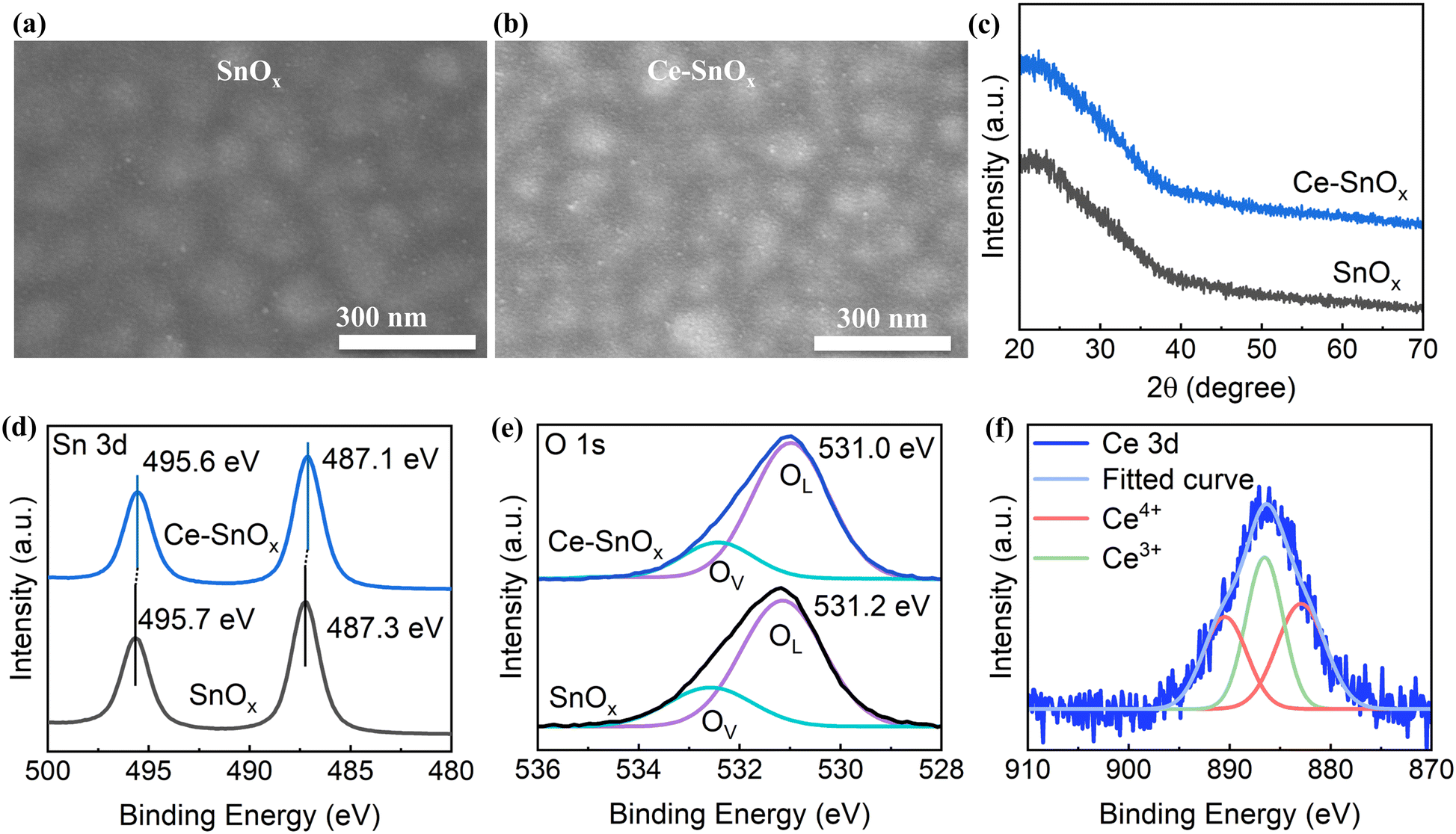 | ||
| Fig. 1 (a) and (b) Top-view SEM images, (c) XRD patterns, (d) Sn 3d XPS, and (e) O 1s XPS spectra of pristine and 2.5 at% Ce-doped SnOx. (f) Ce 3d XPS spectra of 2.5 at% Ce-doped SnOx. | ||
X-ray photoelectron spectroscopy (XPS) measurements were conducted to investigate the chemical states of pristine and Ce-doped SnOx. As seen in the Sn 3d XPS spectrum of SnOx (Fig. 1d), the two peaks at 495.7 eV and 487.3 eV were assigned to Sn 3d3/2 and Sn 3d5/2, respectively. The O 1s XPS spectrum of SnOx exhibited a peak at 931.2 eV (Fig. 1e). Upon Ce doping, the peaks in both Sn 3d and O 1s spectra moved to lower binding energy regions, indicating a possible chemical interaction between Ce and SnOx.16,42 The results also suggested the presence of Sn4+ oxidation states in SnOx and Ce doped SnOx. The peak in the Ce 3d XPS spectrum was resolved into three components representing Ce3+ and Ce4+ oxidation states (Fig. 1f). This result confirmed that Ce ions were successfully incorporated into the host SnOx lattice system. Furthermore, the O 1s XPS peak was deconvoluted into two peaks, one representing the lattice oxygen (OL) in SnOx and the other one originating from the oxygen vacancies or chemisorbed hydroxyl groups (OV). As the Ce doping concentration increased from 0 to 2.5 at%, the ratio of OV to total oxygen decreased from 24.11% to 19.40% (Table S1, ESI†). Thus, the surface oxygen defects of SnOx were passivated upon introducing Ce ions, thereby reducing recombination losses at ETL/perovskite interfaces within PSCs.
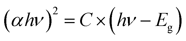
The optical properties of pristine and Ce-doped SnOx samples were also investigated by ultraviolet-visible (UV/Vis) absorption measurements. As displayed in Fig. 2a, the transmittance of both pristine and Ce-doped SnOx was above 80% in the visible light region, which verified the transparency of pristine and Ce-doped SnOx as ETLs for planar PSCs. The transmittance and absorption (Fig. S3, ESI†) changed slightly upon Ce doping. The Tauc's relationship was used to determine the optical band gap (Eg) of SnOx and Ce-doped SnOx, which is described using a formula:
 | (1) |
 | (2) |
 | ||
| Fig. 2 (a) Transmittance, (b) Tauc's plots, (c) and (d) UPS spectra, and (e) valence band XPS spectra of pristine SnOx and 2.5 at% Ce-doped SnOx. (f) Energy band diagram of PSCs based on SnOx and 2.5 at% Ce-doped SnOx ETLs. | ||
The electrical properties of pristine and Ce-doped SnOx thin films were also studied. The conductivity of SnOx increased at first and then decreased when the Ce doping concentration increased from 0 to 10 at% (Fig. S4, ESI†). The conductivity of 2.5 at% Ce-doped SnOx was estimated to be 7.57 × 10⁻⁵ S cm−1 (Fig. 3a), which was about 2.6 times higher than that of pristine SnOx (2.96 × 10⁻⁵ S cm−1). This enhancement originated from the increase in the electron density as well as the passivation of the surface defects in SnOx upon Ce doping.42,45 The improved electrical conductivity of Ce-doped SnOx can boost the charge transfer at ETL/perovskite interfaces, leading to improved short-circuit current density (JSC). The steady-state photoluminescence (PL) and time-resolved photoluminescence (TRPL) measurements were performed to investigate the charge transfer dynamics and examine the perovskite film quality. The perovskite films deposited on Ce-doped SnOx exhibited stronger PL intensities than that deposited on pristine SnOx (Fig. 3b and Fig. S5, ESI†), which indicated that the carrier recombination in Ce–SnOx/perovskite films was effectively suppressed.46 This was further verified by the TRPL results (Fig. 3c). The TRPL decay curves were fitted with a bi-exponential decay function:
 | (3) |
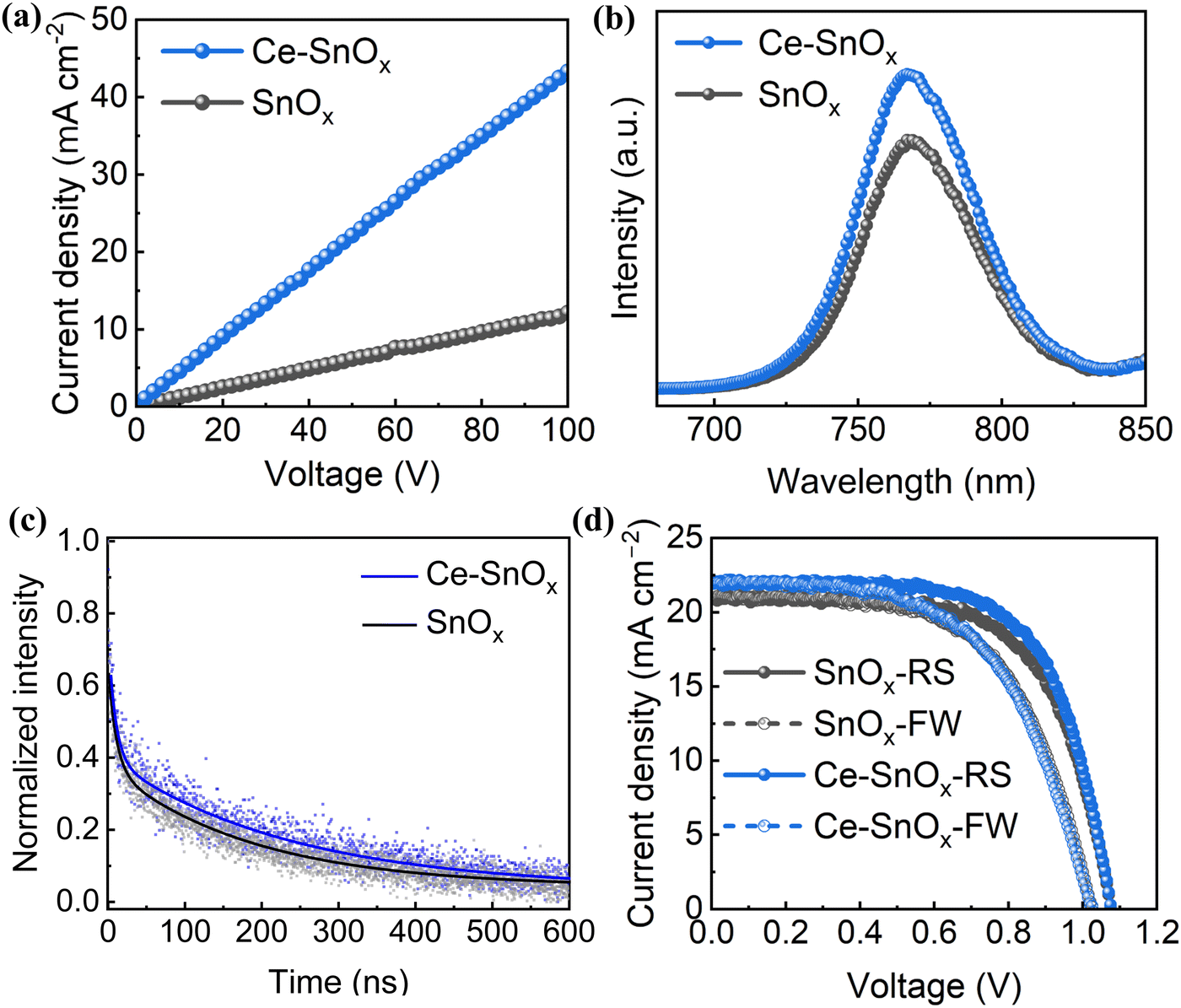 | ||
| Fig. 3 (a) Current–voltage curves for calculating the conductivity of SnOx and 2.5 at% Ce-doped SnOx. (b) PL and (c) normalized TRPL spectra of FTO/SnOx/perovskite and FTO/Ce–SnOx/perovskite. (d) J–V characteristics of the cells with pristine SnOx and 2.5 at% Ce-doped SnOx ETLs. | ||
PSCs with pristine and Ce-doped SnOx ETLs were fabricated to study the effect of Ce doping on the device performance. The current density–voltage (J–V) curves and photovoltaic parameters, i.e., VOC, JSC, fill factor (FF), and PCE are shown in Fig. 3d and Table 1, respectively. An optimum PCE of 15.77% was achieved for the cell with a 2.5 at% Ce-doped SnOx ETL, higher than 14.66% for the cell with pristine SnOx ETL. A significantly improved average PCE of 15.05 ± 0.58% was also delivered by the Ce-doped SnOx (2.5 at%) ETLs compared to 13.87 ± 0.40% for pristine SnOx ETLs (Table S3 and Fig. S6, ESI†), originating from the improvement in all three photovoltaic parameters VOC, JSC, and FF. The improved performance was attributed to enhanced electron extraction and transport and suppressed carrier recombination at ETL/perovskite interfaces, originating from reduced surface defects, enhanced conductivity, and improved energy band alignment between the ETL and the perovskite layer. Further optimization can be carried out to boost the efficiency to higher levels through optimizing each functional layer and interfaces within the PSC devices. The achieved efficiency of 15.77% is still competitive in comparison with the reported values of 13.08% and 18.8% realized by similar inkjet-printed SnO2 ETLs.50,51 In addition, this work provides some insights to ionic doping of SnOx ETLs via a scalable inkjet printing method.
| ETL | Scan direction | PCE (%) | V OC (V) | J SC (mA cm−2) | FF (%) |
|---|---|---|---|---|---|
| SnOx | reverse | 14.66 | 1.08 | 20.96 | 65.0 |
| 2.5 at% Ce–SnOx | reverse | 15.77 | 1.08 | 21.98 | 66.4 |
Conclusions
In summary, inkjet-printed Ce-doped SnOx was successfully fabricated as an effective electron transport layer for planar PSCs. Ce-doped SnOx showed enhanced conductivity and improved energy band alignment with the perovskite layer, contributing to facilitating charge extraction and transport capabilities. Upon Ce doping, the surface defects of SnOx were also passivated. The photoluminescence characterization revealed that the perovskite film deposited on Ce-doped SnOx exhibited a longer decay lifetime, representing the suppression of the carrier recombination within the perovskite film. Consequently, planar PSCs with Ce-doped SnOx (2.5 at%) ETLs delivered an improved PCE of 15.77%, compared to those devices with undoped SnOx ETLs (14.66%). Moreover, this work demonstrated a sustainable and scalable inkjet printing method for the fabrication of efficient planar PSCs.Experimental
Materials
All chemicals were used as received without further modifications. Tin(IV) acetate (Sn(CH3CO2)4) and cerium(III) nitrate hexahydrate (Ce(NO3)3·6H2O, 99.99%) were purchased from Sigma-Aldrich (Darmstadt, Germany). Lead iodide (PbI2, 99.99%) and lead bromide (PbBr2, >98.0%) were purchased from TCI (Tokyo, Japan). Formamidinium iodide (FAI, CH(NH2)2I, >98%) and methylammonium bromide (MABr, CH3NH3Br, >98%) were purchased from Dyenamo (Stockholm, Sweden) and Sigma-Aldrich (Darmstadt, Germany), respectively. Spiro-OMeTAD (99.8%) was purchased from Borun New Material Technology (Ningbo, China). Bis(trifluoromethane)sulfonimide lithium salt (LiTFSI, 99.95%), FK209 (Co(III) TFSI salt, 98%) and 4-tert-butylpyridine (TBP, 98%) were obtained from Sigma-Aldrich (Darmstadt, Germany).Set-up of inkjet printer
A piezoelectric drop-on-demand inkjet system was designed for the printheads from XaarJet in our lab.52,53 Inkjet printing of pristine and Ce-doped SnOx thin films was performed under ambient conditions by employing XJ126/80 printheads which possess 126 active nozzles and can yield a drop volume of 80 pL. A customized waveform was used to form and eject droplets. The printing frequency was set as 283.46 Hz, and the printing resolution was 360 dpi.Inkjet printing of pristine and Ce-doped SnOx thin layers
The ink for printing SnOx thin films was prepared by dissolving tin(IV) acetate in a mixture of 2-propanol and propylene glycol (9/1, v/v) to form a 0.05 M precursor solution. A small amount of ethanolamine was added to improve the acetate solubility. The precursor ink was then inkjet-printed onto substrates which were pre-heated at 60 °C. The as-printed thin films were dried at 60 °C for 5 min and afterwards were annealed inside a furnace at 220 °C for 1 h. Ce-doped SnOx thin films were fabricated in a similar process to pristine SnOx thin films. The only difference lied in the preparation of the precursor ink. A certain amount of a 0.25 M Ce(NO3)3 solution, consisting of Ce(NO3)3·6H2O dissolved in a mixture of 2-propanol and propylene glycol (9/1, v/v), was added to a 0.05 M tin acetate solution prepared as described above. The amount of the added Ce(NO3)3 solution was determined based on the desired doping level, e.g., 50 μL for 2.5 at%. Then, the mixed solution was used for inkjet printing of Ce-doped SnOx thin films. The inkjet printing and post-treatment processes were the same as the fabrication process of pristine SnOx thin films.Device fabrication
FTO glass substrates (13 Ω sq−1, Sigma–Aldrich) were cut into pieces with the dimension of 25 × 15 mm. Each piece was etched at the edge through dripping 2 M HCl aqueous solution onto Zn powder. These substrates were successively sonicated in a detergent solution (5% deconex in water), deionized water, acetone, and 2-propanol for 15 min. Before inkjet printing, FTO substrates were pre-heated at 500 °C for 30 min and afterwards cooled down to room temperature. Compact SnOx or Ce-doped SnOx ETLs were fabricated via inkjet printing as described above. Then, the perovskite layers were fabricated following the procedure reported previously.54 The perovskite precursor was prepared by dissolving PbI2, FAI, PbBr2, and MABr in a mixed solvent (N,N-dimethylformamide/dimethyl sulfoxide = 4/1, v/v) to form a 1.3 M Pb precursor solution. The molar ratio of PbI2/FAI/PbBr2/MABr was 1.1/1/0.2/0.2. Seventy-five μL of the perovskite precursor was spin-coated at 4500 rpm for 30 s. During the spin coating, 125 μL of chlorobenzene was dripped onto the perovskite film at 15 s. The as-deposited perovskite film was immediately dried at 100 °C for 30 min. A hole transport layer was spin-coated at 4000 rpm for 30 s with a precursor consisting of 85.8 mg Spiro-OMeTAD, 35 μL LiTFSI solution (0.6 M), 33.8 μL TBP, and 10 μL FK 209 solution (0.2 M) dissolved in 1 mL chlorobenzene. Finally, an 80 nm-thick Au electrode was thermally evaporated (Edwards Auto 306) onto the substrates.Characterization
The morphology of the pristine and Ce-doped SnOx thin films was studied using a combined focused ion beam/scanning electron microscope (FIB/SEM, FEI Nova 600 Nanolab, FEI Company, Eindhoven, The Netherlands). XRD patterns were obtained employing an X-ray diffractometer (Siemens D5000, Siemens, Munich, Germany) with a Cu Kα radiation (λ = 1.5406 Å). The XPS and UPS measurements were conducted using the K-alpha XPS/UPS system manufactured by Thermo Scientific. For XPS analysis, the spectra were obtained using a monochromatized Al Kα line with a photon energy (hν) of 1486.6 eV. For UPS analysis, a He1 ultraviolet light source with an energy of 21.22 eV was employed. The valence band photoelectron signal originated from the top 2–3 nm of the sample's surface, and the electronic work function of the material's surface was measured. The UV/Vis absorption and transmittance spectra were obtained using a Lambda 750 spectrophotometer. The conductivity of thin films was measured according to the report55 and the details of the measurement were shown in Fig. S7 (ESI†). Current–voltage (I–V) characteristics were collected using a Keithley 2400 instrument. The steady-state PL of perovskite films was investigated using Fluorolog FL 3-22 spectrometer at room temperature (Horiba Jobin Yvon, Longjumeau, France), equipped with a double excitation monochromator, a single emission monochromator (HR320) and a R928P PMT detector. A continuous xenon lamp (450 W) was used for steady state measurements. A supercontinuum laser (Fianium WhiteLase) was employed as a source for the TRPL. For all photoluminescence measurements the excitation wavelength was 500 nm, and the detection wavelength was 765 nm. The active area of the solar cells was defined by a mask of 0.152 cm2 and was illuminated under an AM 1.5 G solar simulator (Newport 91160-1000) with an incident light density of 100 mW cm−2. J–V characteristics of the PSC devices were recorded at a scan rate of 125 mV s−1, using a Keithley 2400 unit.Data availability
The data supporting this article have been included as part of the ESI.†Conflicts of interest
There are no conflicts to declare.Acknowledgements
The authors sincerely acknowledge the valuable discussions with Dr. Jinghua Guo and Dr. Feipeng Yang. This research was funded by China Scholarship Council (No. 201700260217) and Jernkontoret (Stiftelsen Jernkontorsfonden för Bergsvetenskaplig Forskning and Stiftelsen Prvtziska fonden nr 2). Work at the Molecular Foundry was supported by the Office of Science, Office of Basic Energy Sciences, of the U. S. Department of Energy under Contract No. DE-AC02-05CH11231. JG and MJ gratefully acknowledge the support of the Swedish government through the strategic research area STandUP for ENERGY and from Energimyndigheten (Swedish Energy Agency, grant number: 49278-1).References
- S. Y. Park and K. Zhu, Adv. Mater., 2022, 34, 2110438 CrossRef CAS PubMed.
- Q. Jiang, L. Zhang, H. Wang, X. Yang, J. Meng, H. Liu, Z. Yin, J. Wu, X. Zhang and J. You, Nat. Energy, 2016, 2, 16177 CrossRef.
- D. Richards, D. Burkitt, R. Patidar, D. Beynon and T. Watson, Mater. Adv., 2022, 3, 8588–8596 RSC.
- K. Wei, J. Deng, L. Yang, C. Zhang, M. Huang, X. Cai, X. Zhang and J. Zhang, Adv. Energy Mater., 2023, 13, 2203448 CrossRef CAS.
- J. Tian, J. Wu, R. Li, Y. Lin, J. Geng, W. Lin, Y. Wang, Q. Ouyang, Z. Wu, W. Sun, L. Li, Z. Lan and Y. Lin, Nano Energy, 2023, 118, 108939 CrossRef CAS.
- L. Zhang, C. Fu, S. Wang, M. Wang, R. Wang, S. Xiang, Z. Wang, J. Liu, H. Ma, Y. Wang, Y. Yan, M. Chen, L. Shi, Q. Dong, J. Bian and Y. Shi, Adv. Funct. Mater., 2023, 33, 2213961 CrossRef CAS.
- H. Ye, Z. Liu, X. Liu, B. Sun, X. Tan, Y. Tu, T. Shi, Z. Tang and G. Liao, Appl. Surf. Sci., 2019, 478, 417–425 CrossRef CAS.
- P. Sakthivel, S. Foo, M. Thambidurai, P. C. Harikesh, N. Mathews, R. Yuvakkumar, G. Ravi and C. Dang, J. Power Sources, 2020, 471, 228443 CrossRef CAS.
- X. Zhou, W. Zhang, X. Wang, P. Lin, S. Zhou, T. Hu, L. Tian, F. Wen, G. Duan, L. Yu, Y. Xiang, B. Huang and Y. Huang, Appl. Surf. Sci., 2022, 584, 152651 CrossRef CAS.
- H. Chen, D. Liu, Y. Wang, C. Wang, T. Zhang, P. Zhang, H. Sarvari, Z. Chen and S. Li, Nanoscale Res. Lett., 2017, 12, 238 CrossRef PubMed.
- Z. Ma, W. Zhou, Z. Xiao, H. Zhang, Z. Li, J. Zhuang, C. Peng and Y. Huang, Org. Electron., 2019, 71, 98–105 CrossRef CAS.
- J. Song, W. Zhang, D. Wang, K. Deng, J. Wu and Z. Lan, Sol. Energy, 2019, 185, 508–515 CrossRef CAS.
- Y. Bai, Y. Fang, Y. Deng, Q. Wang, J. Zhao, X. Zheng, Y. Zhang and J. Huang, ChemSusChem, 2016, 9, 2686–2691 CrossRef CAS PubMed.
- G. Yang, H. Lei, H. Tao, X. Zheng, J. Ma, Q. Liu, W. Ke, Z. Chen, L. Xiong, P. Qin, Z. Chen, M. Qin, X. Lu, Y. Yan and G. Fang, Small, 2017, 13, 1601769 CrossRef PubMed.
- M. Park, J.-Y. Kim, H. J. Son, C.-H. Lee, S. S. Jang and M. J. Ko, Nano Energy, 2016, 26, 208–215 CrossRef CAS.
- R. Wang, J. Wu, S. Wei, J. Zhu, M. Guo, Q. Zheng, M. Wei and S. Cheng, J. Power Sources, 2022, 544, 231870 CrossRef CAS.
- X. Ren, D. Yang, Z. Yang, J. Feng, X. Zhu, J. Niu, Y. Liu, W. Zhao and S. F. Liu, ACS Appl. Mater. Interfaces, 2017, 9, 2421–2429 CrossRef CAS PubMed.
- Y. W. Noh, J. H. Lee, I. S. Jin, S. H. Park and J. W. Jung, Nano Energy, 2019, 65, 104014 CrossRef CAS.
- W. Cao, J. Zhang, K. Lin, L. Qiu, J. Li, Y. Dong, J. Wang, D. Xia, R. Fan and Y. Yang, Sol. RRL, 2021, 5, 2100058 CrossRef CAS.
- C. Wang, J. Wu, X. Liu, S. Wang, Z. Yan, L. Chen, G. Li, X. Zhang, W. Sun and Z. Lan, J. Alloys Compd., 2021, 886, 161352 CrossRef CAS.
- B. Gu, Y. Du, B. Chen, R. Zhao, H. Lu, Q. Xu and C. Guo, ACS Appl. Mater. Interfaces, 2022, 14, 11264–11272 CrossRef CAS PubMed.
- H. Wang, J. Yuan, J. Xi, J. Du and J. Tian, J. Phys. Chem. Lett., 2021, 12, 9142–9148 CrossRef CAS PubMed.
- C. Liu, M. Guo, H. Su, P. Zhai, K. Xie, Z. Liu, J. Zhang, L. Liu and H. Fu, Appl. Surf. Sci., 2022, 588, 152943 CrossRef CAS.
- L. Yao, M. Zhao, L. Liu, S. Chen, J. Wang, C.-J. Zhao, Z. Jia, S. Pang, X. Guo and T. Jiu, Mater. Chem. Front., 2021, 5, 6913–6922 RSC.
- L. He, H. Su, Z. Li, H. Liu and W. Shen, Adv. Funct. Mater., 2023, 33, 2213963 CrossRef CAS.
- D. Wang, S.-C. Chen and Q. Zheng, J. Mater. Chem. C, 2019, 7, 12204–12210 RSC.
- J. Liang, Z. Chen, G. Yang, H. Wang, F. Ye, C. Tao and G. Fang, ACS Appl. Mater. Interfaces, 2019, 11, 23152–23159 CrossRef CAS PubMed.
- C. Yu, B. Zhang, G. Wang, J. Wang, J. Zhang, P. Chen, C. Li and Y. Duan, Appl. Phys. Lett., 2022, 121, 073501 CrossRef CAS.
- J. H. Lee, S. Lee, T. Kim, H. Ahn, G. Y. Jang, K. H. Kim, Y. J. Cho, K. Zhang, J.-S. Park and J. H. Park, Joule, 2023, 7, 380–397 CrossRef CAS.
- P. Wang, B. Chen, R. Li, S. Wang, N. Ren, Y. Li, S. Mazumdar, B. Shi, Y. Zhao and X. Zhang, ACS Energy Lett., 2021, 6, 2121–2128 CrossRef CAS.
- K. Chen, H. Zhang, H. Tong, L. Wang, L. Tao, K. Wang, Y. Zhang and X. Zhou, Int. J. Hydrogen Energy, 2021, 46, 5677–5688 CrossRef CAS.
- J. Jin, H. Li, W. Bi, C. Chen, B. Zhang, L. Xu, B. Dong, H. Song and Q. Dai, Sol. Energy, 2020, 198, 187–193 CrossRef CAS.
- H. Lu, J. Zhuang, Z. Ma, W. Zhou, H. Xia, Z. Xiao, H. Zhang and H. Li, RSC Adv., 2019, 9, 1075–1083 RSC.
- R. Xu, Y. Li, S. Feng, J. Wang, J. Zhang, X. Zhang, C. Bian, W. Fu, Z. Li and H. Yang, J. Mater. Sci., 2020, 55, 5681–5689 CrossRef CAS.
- Z. Song, W. Xu, Y. Wu, S. Liu, W. Bi, X. Chen and H. Song, Small, 2020, 16, 2001770 CrossRef CAS PubMed.
- D. Hu, H. Tang, X. Zhang, Z. Li, X. Zhu and T. Zhu, Sol. RRL, 2023, 7, 2201129 CrossRef CAS.
- K. Zhao, Y. Zhao, Y. Tan, K. Hu and Z.-S. Wang, ACS Appl. Energy Mater., 2021, 4, 9038–9045 CrossRef CAS.
- F. P. Gokdemir Choi, H. Moeini Alishah and S. Gunes, Appl. Surf. Sci., 2021, 563, 150249 CrossRef CAS.
- S. An, P. Chen, F. Hou, Q. Wang, H. Pan, X. Chen, X. Lu, Y. Zhao, Q. Huang and X. Zhang, Sol. Energy, 2020, 196, 409–418 CrossRef CAS.
- E. Halvani Anaraki, A. Kermanpur, M. T. Mayer, L. Steier, T. Ahmed, S.-H. Turren-Cruz, J. Seo, J. Luo, S. M. Zakeeruddin, W. R. Tress, T. Edvinsson, M. Grätzel, A. Hagfeldt and J.-P. Correa-Baena, ACS Energy Lett., 2018, 3, 773–778 CrossRef CAS.
- B. Parida, A. Singh, A. K. Kalathil Soopy, S. Sangaraju, M. Sundaray, S. Mishra, S. Liu and A. Najar, Adv. Sci., 2022, 9, 2200308 CrossRef PubMed.
- Y. Wang, Y. Li, C. Li, C. Wang, Q. Zhou, L. Liang, Z. Zhang, C. Liu, W. Yu, X. Yu and P. Gao, Small, 2024, 2402531 CrossRef PubMed.
- J. Tauc and A. Menth, J. Non-Cryst. Solids, 1972, 8–10, 569–585 CrossRef CAS.
- S. Song, G. Kang, L. Pyeon, C. Lim, G.-Y. Lee, T. Park and J. Choi, ACS Energy Lett., 2017, 2, 2667–2673 CrossRef CAS.
- P. S. Archana, A. Gupta, M. M. Yusoff and R. Jose, Appl. Phys. Lett., 2014, 105 Search PubMed.
- Q. Jiang, Y. Zhao, X. Zhang, X. Yang, Y. Chen, Z. Chu, Q. Ye, X. Li, Z. Yin and J. You, Nat. Photonics, 2019, 13, 460–466 CrossRef CAS.
- Y. Li, L. Meng, Y. Yang, G. Xu, Z. Hong, Q. Chen, J. You, G. Li, Y. Yang and Y. Li, Nat. Commun., 2016, 7, 10214 CrossRef CAS PubMed.
- J. Fu, J. Zhang, T. Zhang, L. Yuan, Z. Zhang, Z. Jiang, Z. Huang, T. Wu, K. Yan, L. Zhang, A. Wang, W. Ji, Y. Zhou and B. Song, ACS Nano, 2023, 17, 2802–2812 CrossRef CAS PubMed.
- F. Cai, J. Lin, W. Pan, S. Zhu, W. Li, Y. Du, J. Liu, M. Yang and J. Wu, ACS Appl. Energy Mater., 2022, 5, 8501–8509 CrossRef CAS.
- A. H. Ghahremani, D. Ratnayake, A. Sherehiy, D. O. Popa and T. Druffel, Energy Technol., 2021, 9, 2100452 CrossRef CAS.
- V. Rohnacher, F. Ullrich, H. Eggers, F. Schackmar, S. Hell, A. Salazar, C. Huck, G. Hernandez-Sosa, U. W. Paetzold, W. Jaegermann and A. Pucci, Adv. Mater. Technol., 2021, 6, 2000282 CrossRef CAS.
- M. Fang, Doctoral thesis, KTH Royal Institute of Technology, 2012.
- Y. Wu, Doctoral thesis, KTH Royal Institute of Technology, 2010.
- W. Zhang, P. Liu, A. Sadollahkhani, Y. Li, B. Zhang, F. Zhang, M. Safdari, Y. Hao, Y. Hua and L. Kloo, ACS Omega, 2017, 2, 9231–9240 CrossRef CAS PubMed.
- C. Chen, W. Zhang, J. Cong, M. Cheng, B. Zhang, H. Chen, P. Liu, R. Li, M. Safdari, L. Kloo and L. Sun, ACS Energy Lett., 2017, 2, 497–503 CrossRef CAS.
Footnote |
| † Electronic supplementary information (ESI) available. See DOI: https://doi.org/10.1039/d4ma00094c |
| This journal is © The Royal Society of Chemistry 2024 |