 Open Access Article
Creative Commons Attribution 3.0 Unported Licence
Characterization of reactively sputter deposited CuCrO2 thin films using Cu and Cr targets
Akash Hari
Bharath
 * and
Kalpathy B.
Sundaram
Department of Electrical and Computer Engineering, University of Central Florida, Orlando, FL 32826, USA. E-mail: akash.hari.bharath@ucf.edu
First published on 22nd October 2024
Abstract
In this research, single phase delafossite CuCrO2 thin films were successfully synthesized using dual sputtering technique. A DC source was employed for the copper target, whereas the chromium target was sputtered using an RF source with oxygen acting as the reactive gas. The films were sputtered on a quartz substrate at 400 °C. The sputtering power for chromium was maintained at 100 W, while the power for copper ranged from 10 W to 40 W. Following deposition, the films were annealed in a nitrogen environment for 10 hours at 800 °C. XRD examination confirmed that single-phase CuCrO2 was achieved with a copper target power of 20 W. The findings of the XRD investigation were further validated by XPS analysis. Cu![[thin space (1/6-em)]](https://www.rsc.org/images/entities/char_2009.gif) :
:![[thin space (1/6-em)]](https://www.rsc.org/images/entities/char_2009.gif) Cr at% composition ratio of 1
Cr at% composition ratio of 1![[thin space (1/6-em)]](https://www.rsc.org/images/entities/char_2009.gif) :
:![[thin space (1/6-em)]](https://www.rsc.org/images/entities/char_2009.gif) 1
1![[thin space (1/6-em)]](https://www.rsc.org/images/entities/char_2009.gif) :
:![[thin space (1/6-em)]](https://www.rsc.org/images/entities/char_2009.gif) 04 was obtained when deposited at a power of 20 W. SEM grain sizes ranged from 100 nm to 150 nm optical studies indicated an optical transmission of 57.5% and a bandgap of 3.08 eV. The single-phase film demonstrated a resistivity of 28.6 Ω cm.
04 was obtained when deposited at a power of 20 W. SEM grain sizes ranged from 100 nm to 150 nm optical studies indicated an optical transmission of 57.5% and a bandgap of 3.08 eV. The single-phase film demonstrated a resistivity of 28.6 Ω cm.
Introduction
Transparent conducting oxides (TCOs) are wide-bandgap semiconductors known for their good optical transmittance in the visible spectrum and high electrical conductivity.1,2 Due to these characteristics, they are commonly employed in optical devices like LEDs, displays, solar cells, and sensors.3–6 p-Type and n-type TCOs have the potential to be utilized in touch panels for applications in smartphones and hospitals.7 Because of their excellent conductivity, n-type TCOs are commonly employed as electrodes.8 Numerous studies have been carried out on n-type TCOs, like Al-doped ZnO (AZO),9–12 Sc-doped ZnO,13,14 and Sn-doped In2O3 (ITO).15,16 However, the limited research on p-type TCOs hinders the advancement of transparent electronics.17–19 Transparent electronics with active devices need a combination of p- and n-type semiconductor layers. As a result, they require a p-type counterpart.Synthesizing p-type TCOs has proven to be challenging. This difficulty arises because holes are deeply localized at the O-2p oxygen level. The metallic atoms valence orbitals atoms are at much higher energy levels compared to the O-2p levels, complicating the creation of effective p-type TCOs.20,21 Research indicates that metal oxides possess considerably fewer valence band electrons compared to metals. While doping has been explored as a potential solution, the presence of highly electronegative oxygen ions impedes hole mobility due to the large energy barrier required for hole delocalization.22–24 The concept of chemical modulation of the valence band (CMVB) could be utilized to address this issue.20 Incorporating cations like Cu+, which form strong covalent bonds with oxygen ions, can effectively elevate the oxygen 2p energy level. This reduction in Coulombic attraction between holes and oxygen ions facilitates enhanced hole mobility within the crystal lattice.22 Additionally, the closed shell of Cu 3d10 helps to avoid coloration, thereby preserving optical transparency.25
Films produced using the CMVB concept are referred to as delafossites. Ag+ or Cu+ are employed as cations in this process. Research has shown that films incorporating Ag+ cations generally display very high electrical resistivity (104–106 Ω cm).26 The extremely low carrier mobility is caused by the energy misalignment between the O 2p and Ag 4d orbitals.27 Cu-based delafossites are obtained by incorporating Cu+ cations. These Cu-based delafossites, with a general formula of CuMO2 (where M represents trivalent cations like Cr3+, In3+, Ga3+, Sc3+, and Y3+), have demonstrated promising properties.28 P-type TCOs, especially Cu-based delafossites, have seen a recent surge in attention.29–31 Cu-based delafossites have been shown to have fairly high optical transparency (60–85%).25,32
CuCrO2 is part of the Cu-based delafossite family and is widely studied for its photovoltaic, optical, and electrical characteristics.33–35 It possesses a high bandgap and demonstrates excellent optical transparency along with high hole mobility.2,36 Therefore, p-type delafossite CuCrO2 was chosen as the material for this research. In the past, there have been a few studies on CuCrO2 films. Tripathi et al. have utilized atomic layer deposition (ALD) technique. In their work, they have used copper 2,2,6,6-tetramethyl-3,5-heptanedionate (Cu(thd)2) and chromium acetyl acetonoate (Cr(acac)3) as the precursors.37 The deposited films were later annealed at 600–800 °C in a rapid thermal annealing furnace in Ar atmosphere. Typically, deposition rates are very slow in ALD method. Chiba et al. synthesized CuCrO2 through RF magnetron sputtering using a stoichiometric CuCrO2 ceramic target.38
In this work, CuCrO2 thin films were synthesized using dual-target RF magnetron sputtering using Cu and Cr targets. This dual-target technique provides the flexibility of adjusting the composition of the films and allows precise control over the material ratio by varying the sputtering power of each target. Additionally, it ensures excellent adhesion over large surface areas without the need for specialized precursors, which are often required for chemical vapor deposition.39
Experimental
Deposition of CuCrO2 thin films
CuCrO2 thin films were deposited using a dual-target magnetron reactive sputtering, with an AJA International ultra-high vacuum system equipped with both DC and RF power sources. High-purity copper and chromium targets (99.99% purity) were sputtered onto quartz substrates cleaned using acetone, methanol, and deionized water, followed by drying with nitrogen gas. Ultra-high purity oxygen was used as the reactive gas with a flow rate of 1 sccm, while the argon flow rate was 20 sccm. Due to the tool's limitation to a single DC power source, the chromium target was operated under RF power (13.56 MHz) at a constant power of 100 W, while the copper target was operated under DC power with varying power levels from 10 W to 40 W. The deposition was initiated upon reaching a base pressure of 5 × 10⁻⁷ torr. The thickness of all the samples was around 2000 Å. To ensure uniform film thickness, the substrate holder was rotated at a constant speed of 20 rpm. The deposition pressure was held constant at 10 mTorr, whereas the substrate temperatures during deposition were kept at 300 °C and 400 °C. Post-deposition annealing was performed in a tube furnace under a nitrogen atmosphere for 10 hours at 800 °C. During the annealing process, the gas flow rate was regulated at 300 sccm. Even though the films were annealed for 4 hours and 8 hours, it was found that post-deposition annealing the films for 10 hours at 800 °C exhibited optimal properties. Table 1 summarizes the deposition parameters utilized in this study.| Deposition parameter | Specification |
|---|---|
| Base pressure | 5 × 10⁻⁷ torr |
| Deposition pressure | 10 mTorr |
| Sputtering gas/flow rate | Ar/20 sccm |
| Reactive gas/flow rate | O2/1 sccm |
| Cu power | 10 W, 20 W, 30 W and 40 W |
| Cr power | 100 W |
| Substrate temperature | 300 °C and 400 °C |
| Thickness of deposited film | 200 nm |
| Annealing temperature | 800 °C |
| Annealing time | 4, 8, and 10 hours |
| Annealing gas and flow rate | N2 at 300 sccm |
Film characterization
The films thickness was determined using a Veeco Dektak 150 surface profilometer. X-ray diffraction analysis (XRD) analysis was conducted using the PANalytical Empyrean XRD system with a Cu radiation source operating at 45 kV and 40 mA. Diffraction patterns were recorded in the 2θ range of 25°–70°, and phase information was analyzed using HighScore Plus software version 4.5. The composition of the film was analyzed using ESCALAB 250 Xi + X-ray photoelectron spectroscopy (XPS) equipped with a monochromatic Al Kα source (1486.7 eV). Prior to XPS measurements, an inbuilt EX06 ion source was used for ion milling to remove surface oxygen. Thermo Fischer Scientific Avantage software was employed for XPS peak fitting and analysis. Surface morphology was analyzed using a Zeiss Ultra-55 scanning electron microscope (SEM). Optical transmission across wavelengths from 200 to 800 nm was analyzed using a Cary 100 UV-Vis spectrometer, and the band gap of the films was determined using the Tauc plot technique. The conductivity type of the annealed films was assessed using the hot probe method, and electrical resistivity was measured using the 4-point probe method.Results and discussion
Deposition rate studies
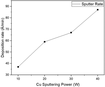
Fig. 1 shows the deposition rate trend at 400 °C substrate temperature for various copper sputtering power levels. It is observed that as the sputtering power applied to the copper target increased, the sputtering rate also increased. While films deposited at 10 W exhibited a lower deposition rate of approximately 37 Å min−1, those produced at 40 W demonstrated a significantly higher rate of 87 Å min−1. The increase in the sputtering rate is due to the fact that higher sputtering power releases more copper atoms from the target.40 Based on the deposition rates, the duration of sputtering was adjusted to attain a thickness of around 2000 Å for all the samples.XRD analysis
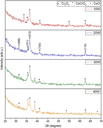
The films were deposited at 300 °C and 400 °C. Since the films annealed for 4 hours and 8 hours in N2 ambiance after deposition did not show any significant peaks pertaining to the CuCrO2 phase, all post-deposition was done for 10 hours. Films prepared by depositing at 300 °C and subsequently annealing at 800 °C, using a copper sputtering power of 10 W, exhibited a more Cr2O3-rich phase. A mixed phase of Cr2O3 and CuCrO2 was shown in the film when the power to the copper target was raised to 20 W. A film rich in the CuO phase was produced by raising the power to 30 W. As these films did not yield optimal results, only the films deposited at 400 °C were subjected to further characterization.The XRD diffractograms of films deposited with different Cu sputtering powers at 400 °C substrate temperature and then annealed at 800 °C are shown in Fig. 2. The amorphous quartz peak observed in all films between 18° and 25° was removed by adjusting the 2θ range. The as-deposited films displayed no diffraction peaks, indicating their amorphous nature. This absence of identifiable peaks was due to insufficient thermal energy during deposition, which impeded crystallization. However, all annealed films showed distinct diffraction peaks, indicating they were nanocrystalline in structure. Films deposited with a copper power of 10 W exhibited peaks corresponding to CuCrO2, along with some peaks associated with Cr2O3. When the copper power was raised to 20 W, the Cr2O3 peaks disappeared, resulting in a single-phase CuCrO2 film. The diffraction peaks for this film were consistent with the delafossite CuCrO2 structure (ICDD: 98-016-3253). The diffraction peaks observed at 2θ angles of 31.37°, 35.65°, 36.5°, 41.14°, and 62.63° were indexed to the (006), (101), (012), (104), and (110), respectively. Eqn (1) describes the chemical reaction involved in the formation of CuCrO2.41
| Cu2O(s) + Cr2O3(s) → 2CuCrO2(s) | (1) |
The films single-phase structure changed to a two-phase structure when the Cu sputtering power was raised to 30 W and 40 W, most likely as a result of the films increasing Cu concentration. At 30 W, peaks corresponding to CuO began to appear, and these peaks became more pronounced at 40 W. This trend indicates a shift from a Cr2O3-rich phase at lower power levels to a CuO-rich phase at higher powers. Therefore, it can be concluded that a single-phase delafossite structure of CuCrO2 thin films was achieved at a Cu sputtering power of 20 W, with no detectable peaks of CuO or Cr2O3.
XPS analysis
Fig. 3 presents the XPS analysis of the single-phase CuCrO2 thin film. The spectrometer's built-in copper sample was utilized for automatic calibration of the binding energy. The film's survey spectrum, displayed in Fig. 3a, confirms the presence of peaks corresponding solely to Cu, Cr, and O. The individual core level spectra for Cu-2p, Cr-2p, and O-1s are illustrated in Fig. 3b–d. Table 2 details the oxidation states, full-width half maximum (FWHM), satellite peak position, peak positions, and associated binding energies for the CuCrO2 film.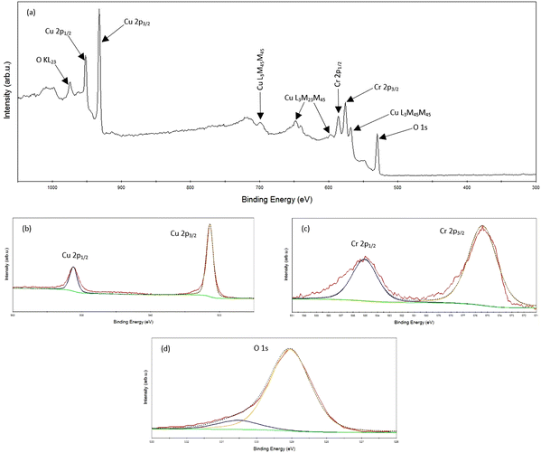 | ||
| Fig. 3 XPS spectra of the CuCrO2 film deposited with a copper sputtering power of 20 W: (a) survey spectrum; (b) Cu-2p state; (c) Cr-2p state; (d) O-1s state. | ||
| Peak | Oxidation state | Binding energy (eV) | Satellite peak (eV) | FWHM (eV) |
|---|---|---|---|---|
| Cu 2p3/2 | Cu1+ | 931.40 | — | 1.18 |
| Cu 2p1/2 | Cu1+ | 951.20 | — | 1.28 |
| Cr 2p3/2 | Cr3+ | 575.40 | — | 2.76 |
| Cr 2p1/2 | Cr3+ | 585.06 | — | 2.45 |
There are two phases of copper chromium oxide: CuCrO2 (delafossite structure) and CuCr2O4 (spinel structure).41,42 Previous studies have established that copper exhibits a +2 oxidation state in CuCr2O4 and a +1 oxidation state in CuCrO2.43 The satellite peaks differentiate between the core level spectra of Cu1+ and Cu2+ species. Specifically, satellite peaks are absent for the Cu1+ species but present for the Cu2+ species.44–46
XPS analysis of the Cu 2p core level spectrum (Fig. 3b) reveals peaks at binding energies of 951.2 eV and 931.4 eV, corresponding to the Cu 2p3/2 and Cu 2p1/2 states, respectively. The absence of satellite peaks in the 940–950 eV region indicates the lack of Cu2+ species in the film. The Cr 2p core level spectrum (Fig. 3c) exhibits a doublet with peaks at 585.06 eV and 575.04 eV, attributed to the Cr 2p1/2 and Cr 2p3/2 states, respectively. The O 1s core level spectrum (Fig. 3d) reveals a peak at 529.05 eV, which is associated with lattice oxygen in CuCrO2.34 A peak detected at 530.53 eV corresponds to chemisorbed oxygen. These findings collectively suggest that the predominant oxidation states of copper and chromium cations are +1 and +3, respectively. The observed peak positions are consistent with previous studies.46,47
The Cu![[thin space (1/6-em)]](https://www.rsc.org/images/entities/char_2009.gif) :
:![[thin space (1/6-em)]](https://www.rsc.org/images/entities/char_2009.gif) Cr at% ratio of films obtained using different copper sputtering powers were studied. Films sputtered with a Cu sputtering power of 10 W exhibited a ratio of 1
Cr at% ratio of films obtained using different copper sputtering powers were studied. Films sputtered with a Cu sputtering power of 10 W exhibited a ratio of 1![[thin space (1/6-em)]](https://www.rsc.org/images/entities/char_2009.gif) :
:![[thin space (1/6-em)]](https://www.rsc.org/images/entities/char_2009.gif) 1.29. As anticipated, the copper content increased with higher sputtering power. The highest Cu
1.29. As anticipated, the copper content increased with higher sputtering power. The highest Cu![[thin space (1/6-em)]](https://www.rsc.org/images/entities/char_2009.gif) :
:![[thin space (1/6-em)]](https://www.rsc.org/images/entities/char_2009.gif) Cr at% ratio of 1
Cr at% ratio of 1![[thin space (1/6-em)]](https://www.rsc.org/images/entities/char_2009.gif) :
:![[thin space (1/6-em)]](https://www.rsc.org/images/entities/char_2009.gif) 0.57 was observed in the film deposited at a copper power of 40 W. Notably, the single-phase CuCrO2 film exhibited a nearly stoichiometric ratio of 1
0.57 was observed in the film deposited at a copper power of 40 W. Notably, the single-phase CuCrO2 film exhibited a nearly stoichiometric ratio of 1![[thin space (1/6-em)]](https://www.rsc.org/images/entities/char_2009.gif) :
:![[thin space (1/6-em)]](https://www.rsc.org/images/entities/char_2009.gif) 1.04. The film sputtered with a copper power of 30 W had a ratio of 1
1.04. The film sputtered with a copper power of 30 W had a ratio of 1![[thin space (1/6-em)]](https://www.rsc.org/images/entities/char_2009.gif) :
:![[thin space (1/6-em)]](https://www.rsc.org/images/entities/char_2009.gif) 0.73. These results validate the successful synthesis of a pure-phase delafossite CuCrO2.
0.73. These results validate the successful synthesis of a pure-phase delafossite CuCrO2.
Morphology studies
SEM images of the films deposited at 400 °C substrate temperature employing different copper sputtering powers are shown in Fig. 4a–d. The images were taken at a magnification of 50 K X. The images reveal distinct grains, confirming the nano-crystallinity previously observed in the XRD analysis. A systematic increase in grain size was observed with an increase in sputtering power. Films sputtered with a copper power of 10 W exhibited an average grain size of 99.2 nm. Single-phase CuCrO2 films deposited at 20 W exhibited an average grain size of 110.05 nm. Increasing the sputtering power to 30 W and 40 W resulted in larger grain sizes of 132.81 nm and 153.62 nm, respectively.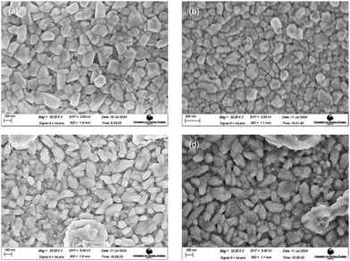 | ||
| Fig. 4 SEM images of films deposited with a copper sputtering power of (a) 10 W, (b) 20 W, (c) 30 W and (d) 40 W. | ||
Optical studies
 | (2) |
 | (3) |
| Copper sputtering power (W) | Bandgap (eV) |
|---|---|
| 10 | 3.15 |
| 20 | 3.08 |
| 30 | 2.98 |
| 40 | 2.89 |
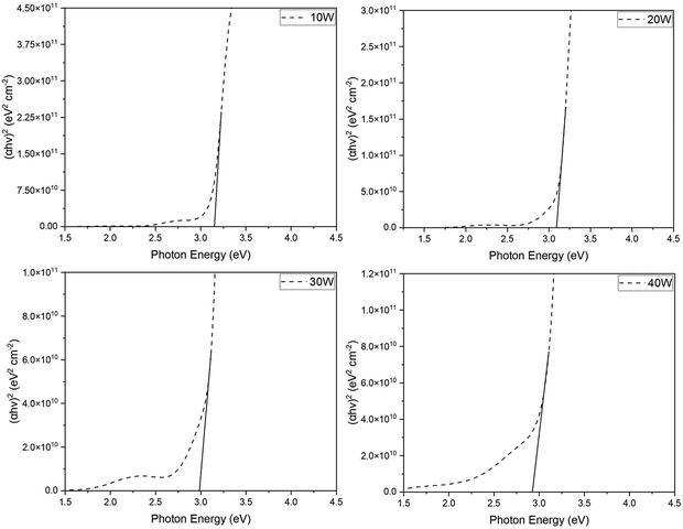
As seen in Fig. 6 and summarized in Table 3, the optical bandgap reduces as copper sputtering power increases. The film deposited at the lowest copper power of 10 W exhibited the highest optical bandgap of 3.15 eV. Conversely, the film deposited at 40 W displayed the lowest optical bandgap at 2.89 eV. The observed reduction in optical bandgap in the corresponding films may be attributed to the fact that Cr2O3 is reported to have a higher bandgap than CuO, which was observed in these films.59–62 The single-phase CuCrO2 thin film exhibited an optical bandgap of 3.08 eV, aligning with previously reported values.63–67
Electrical studies
Electrical studies were conducted on all the films deposited at 400 °C to see how the variance in copper sputtering power affected the films electrical resistance. The observed p-type conductivity in copper-based delafossites, including CuCrO2, CuInO2, and CuGaO2, is attributed to intrinsic defects within the copper lattice, such as interstitial oxygen ions and/or copper vacancies.68,69 The hot probe test further verified this, indicating p-type behavior in all the films.The film with the highest resistivity, measuring around 726 Ω cm, was seen in the film deposited with a copper sputtering power of 10 W. The high resistivity of the film is due to the presence of Cr2O3 in these films. Cr2O3 is a dielectric material known for its high electrical resistivity.70,71 In contrast, the film deposited at 20 W demonstrated the lowest resistivity of 28.6 Ω cm. This low resistivity is attributed to the single-phase property of the delafossite CuCrO2 structure, as verified by the XRD analysis. Among all copper-based delafossites, CuCrO2 shows the lowest resistivity.25 Increasing the sputtering power to 30 W and 40 W resulted in higher resistivities of 56.2 Ω cm and 101.8 Ω cm, respectively. This increase is associated with the formation of a two-phase composition comprising CuO and CuCrO2, deviating from the single-phase structure. Previous reports indicate that CuO can exhibit increased resistivity, reaching up to 104 Ω cm at annealing temperatures above 650 °C.1 However, the films sputtered with a power of 30 W and 40 showed significantly low resistivity, most likely due to the coexistence of the CuO and CuCrO2 phases.
Conclusion
In this work, Cu and Cr targets were successfully used to deposit single phase delafossite CuCrO2 thin films using dual sputtering technique. By varying copper sputtering power while maintaining chromium power at 100 W, followed by annealing at 800 °C in an N2 atmosphere, the morphological, electrical, structural, and optical properties of the films were investigated and documented. XRD analysis confirmed the formation of Cr2O3-rich and CuO-dominant phases at lower and higher copper sputtering powers, respectively. Optimal conditions for single-phase CuCrO2 were achieved at a copper sputtering power of 20 W, supported by XPS analysis indicating the absence of Cu2+. Near-stoichiometric Cu![[thin space (1/6-em)]](https://www.rsc.org/images/entities/char_2009.gif) :
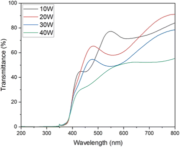
:![[thin space (1/6-em)]](https://www.rsc.org/images/entities/char_2009.gif) Cr ratios were obtained at this power. SEM images revealed an increase in grain size with higher sputtering power. Optical transmission studies showed a decrease in transmittance with increasing copper content. The single-phase CuCrO2 film had a bandgap of 3.08 eV and an average optical transmission of around 57.5%. The film deposited at 20 W had the lowest resistivity of 28.6 Ω cm. This low resistivity highlights its potential as a promising material for transparent electronics, including thin-film transistors and diodes.
Cr ratios were obtained at this power. SEM images revealed an increase in grain size with higher sputtering power. Optical transmission studies showed a decrease in transmittance with increasing copper content. The single-phase CuCrO2 film had a bandgap of 3.08 eV and an average optical transmission of around 57.5%. The film deposited at 20 W had the lowest resistivity of 28.6 Ω cm. This low resistivity highlights its potential as a promising material for transparent electronics, including thin-film transistors and diodes.
Data availability
All the references/data used for this research are mentioned on the reference section of the paper.Conflicts of interest
There are no conflicts to declare.Acknowledgements
The authors would like to acknowledge the NSF MRI: ECCS: 1726636 and MCF-AMPAC facility, MSE, and CECS for the XPS use.References
- L. Hu, et al., Design strategy for p-type transparent conducting oxides, J. Appl. Phys., 2020, 128(14), 140902 CrossRef CAS.
- J. Robertson, et al., Electronic Structure of p-Type Conducting Transparent Oxides, Thin Solid Films, 2002, 411, 96–100 CrossRef CAS.
- A. Stadler, Transparent Conducting Oxides-An Up-To-Date Overview, Materials, 2012, 5(4), 661–683 CrossRef PubMed.
- J.-H. Lan, et al., Patterning of transparent conducting oxide thin films by wet etching for a-Si:H TFT-LCDs, J. Electron. Mater., 1996, 25, 1806–1817 CrossRef CAS.
- A. K. Saikumar, S. D. Nehate and K. B. Sundaram, Review—RF Sputtered Films of Ga2O3, ECS J. Solid State Sci. Technol., 2019, 8(7), Q3064 CrossRef CAS.
- S. Nehate, A. K. Saikumar and K. B. Sundaram, A review of recent developments in aluminum gallium oxide thin films and devices, Crit. Rev. Solid State Mater. Sci, 2021, 538–569 Search PubMed.
- T.-W. Chiu, et al., Antibacterial property of CuCrO2 thin films prepared by RF magnetron sputtering deposition, Vacuum, 2013, 87, 174–177 CrossRef CAS.
- A. K. Saikumar, S. Sundaresh and K. B. Sundaram, Preparation and characterization of p-type copper gallium oxide (CuGaO2) thin films by dual sputtering using Cu and Ga2O3 targets, ECS J. Solid State Sci. Technol., 2022, 11(6), 065010 CrossRef CAS.
- F. Shan and Ys Yu, Band gap energy of pure and Al-doped ZnO thin films, J. Eur. Ceram. Soc., 2004, 24, 1869–1872 CrossRef CAS.
- F. Maldonado and A. Stashans, Al-doped ZnO: Electronic, electrical and structural properties, J. Phys. Chem. Solids, 2010, 71(5), 784–787 CrossRef CAS.
- J. R. Phelps, et al., Comparison of RF and High Impulse Magnetron Sputtered Gallium-Doped Zinc Oxide Thin Films, Coatings, 2023, 13(1), 71 CrossRef CAS.
- B. P. Shantheyanda, K. B. Sundaram and N. S. Shiradkar, Studies on the effect of hydrogen doping during deposition of Al: ZnO films using RF magnetron sputtering, Mater. Sci. Eng., B, 2012, 177(20), 1777–1782 CrossRef CAS.
- S. C. Dixon, et al., Transparent conducting n-type ZnO:Sc – synthesis, optoelectronic properties and theoretical insight, J. Mater. Chem. C, 2017, 5(30), 7585–7597 RSC.
- M. Samadi, et al., Recent progress on doped ZnO nanostructures for visible-light photocatalysis, Thin Solid Films, 2016, 605, 2–19 CrossRef CAS.
- H. R. Fallah, et al., The effect of annealing on structural, electrical and optical properties of nanostructured ITO films prepared by e-beam evaporation, Mater. Res. Bull., 2007, 42(3), 487–496 CrossRef CAS.
- J. George and C. S. Menon, Electrical and optical properties of electron beam evaporated ITO thin films, Surf. Coat. Technol., 2000, 132(1), 45–48 CrossRef CAS.
- S. Sundaresh, A. H. Bharath and K. B. Sundaram, Synthesis and Characterization of Radio-Frequency-Sputtered Delafossite Copper Indium Oxide (CuInO2) Thin Films, ECS J. Solid State Sci. Technol., 2023, 12(4), 043010 CrossRef CAS.
- A. K. Saikumar, et al., Preparation and Characterization of Radio Frequency Sputtered Delafossite p-type Copper Gallium Oxide (p-CuGaO2) Thin Films, ECS J. Solid State Sci. Technol., 2022, 11(2), 023005 CrossRef.
- A. H. Bharath, A. K. Saikumar and K. B. Sundaram, Deposition and Optical Characterization of Sputter Deposited p-Type Delafossite CuGaO2 Thin Films Using Cu2O and Ga2O3 Targets, Materials, 2024, 17(7), 1609 CrossRef CAS PubMed.
- H. Kawazoe, et al., P-type electrical conduction in transparent thin films of CuAlO < SUB > 2 </SUB >, Nature, 1997, 389, 939–942 CrossRef CAS.
- G. Hautier, et al., Identification and design principles of low hole effective mass p-type transparent conducting oxides, Nat. Commun., 2013, 4(1), 2292 CrossRef PubMed.
- A. N. Banerjee and K. K. Chattopadhyay, Recent developments in the emerging field of crystalline p-type transparent conducting oxide thin films, Prog. Cryst. Growth Charact. Mater., 2005, 50(1), 52–105 CrossRef CAS.
- R. Afre, et al., Transparent Conducting Oxide Films for Various Applications: A Review, Rev. Adv. Mater. Sci., 2019, 53, 79–89 Search PubMed.
- K. Zhang, et al., P-type transparent conducting oxides, J. Phys. Cond. Matter., 2016, 28, 383002 CrossRef PubMed.
- M. Moreira, et al., A review on the p-type transparent Cu–Cr–O delafossite materials, J. Mater. Sci., 2022, 57(5), 3114–3142 CrossRef CAS.
- R. Nagarajan, et al., p-Type conductivity in the delafossite structure, Int. J. Inorg. Mater., 2001, 3(3), 265–270 CrossRef CAS.
- M. F. Iozzi, et al., Structural and electronic properties of transparent conducting delafossite: a comparison between the AgBO2 and CuBO2 families (B = Al, Ga, In and Sc, Y), RSC Adv., 2015, 5(2), 1366–1377 RSC.
- R.-S. Yu and Y.-C. Lee, Effects of annealing on the optical and electrical properties of sputter-deposited CuGaO2 thin films, Thin Solid Films, 2018, 646, 143–149 CrossRef CAS.
- M. Han, et al., Structural, optical and electrical properties of delafossite CuGaO2 films grown by sol–gel method, Eighth International Conference on Thin Film Physics and Applications, 2013, SPIE Search PubMed.
- J. Ahmed and Y. Mao, Synthesis, characterization and electrocatalytic properties of delafossite CuGaO2, J. Solid State Chem., 2016, 242, 77–85 CrossRef CAS.
- Z. Xu, et al., Remarkable Photocurrent of P-type Dye-sensitized Solar Cell Achieved by Size Controlled CuGaO2 Nanoplates, J. Mater. Chem. A, 2013, 2968–2976 Search PubMed.
- N. Zhang, J. Sun and H. Gong, Transparent p-type semiconductors: copper-based oxides and oxychalcogenides, Coatings, 2019, 9(2), 137 CrossRef.
- L. Bottiglieri, Out of stoichiometry CuCrO2 as transparent p-type semiconductor for photovoltaics and transparent electronics, 2022, Université Grenoble Alpes Search PubMed.
- F. Lin, et al., Magnetic, electrical and optical properties of p-type Fe-doped CuCrO2 semiconductor thin films, J. Alloys Compd., 2013, 581, 502–507 CrossRef CAS.
- L. Deng, et al., Improved ferromagnetic behavior and novel near-infrared photoluminescence in Mg/Mn-codoped CuCrO2 ceramics, J. Mater. Sci., 2016, 51, 7491–7501 CrossRef CAS.
- X. Nie, S.-H. Wei and S. Zhang, Bipolar Doping and Band-Gap Anomalies in Delafossite Transparent Conductive Oxides, Phys. Rev. Lett., 2002, 88, 066405 CrossRef PubMed.
- T. Tripathi and M. Karppinen, Structural optical and electrical transport properties of ALD-fabricated CuCrO2 films, Phys. Procedia, 2015, 75, 488–494 CrossRef CAS.
- H. Chiba, T. Kawashima and K. Washio, Optical and structural properties of CuCrO2 thin films on c-face sapphire substrate deposited by reactive RF magnetron sputtering, Mater. Sci. Semicond. Process., 2017, 70, 234–238 CrossRef CAS.
- A. K. Saikumar, et al., Properties of RF Magnetron-Sputtered Copper Gallium Oxide (CuGa2O4) Thin Films, Coatings, 2021, 11(8), 921 CrossRef CAS.
- M.-T. Le, et al., Effect of sputtering power on the nucleation and growth of Cu films deposited by magnetron sputtering, Mater. Trans., 2010, 51(1), 116–120 CrossRef CAS.
- V. Novikov, et al., Solution Combustion Synthesis of nanoscale Cu-Cr-O spinels: Mechanism, properties and catalytic activity in CO oxidation, Ceram. Int., 2017, 43(15), 11733–11742 CrossRef CAS.
- J. Schorne-Pinto, et al., Thermodynamic and structural properties of CuCrO2 and CuCr2O4: experimental investigation and phase equilibria modeling of the Cu–Cr–O system. The, J. Phys. Chem. C, 2021, 125(27), 15069–15084 CrossRef CAS.
- H.-Y. Chen and K. Chang, Influence of post-annealing conditions on the formation of delafossite-CuCrO2 films, ECS J. Solid State Sci. Technol., 2013, 2(3), P76 CrossRef CAS.
- H.-Y. Chen, W.-J. Yang and K. Chang, Characterization of delafossite-CuCrO2 thin films prepared by post-annealing using an atmospheric pressure plasma torch, Appl. Surf. Sci., 2012, 258(22), 8775–8779 CrossRef CAS.
- S. Wu, et al., Effect of deposition atmosphere on the structure and properties of Mg doped CuCrO2 thin films prepared by direct current magnetron sputtering, Thin Solid Films, 2015, 595, 124–128 CrossRef CAS.
- J. Crêpellière, et al., Transparent conductive CuCrO2 thin films deposited by pulsed injection metal organic chemical vapor deposition: Up-scalable process technology for an improved transparency/conductivity trade-off, J. Mater. Chem. C, 2016, 4(19), 4278–4287 RSC.
- L. Bottiglieri, et al., Out of stoichiometry CuCrO2 films as a promising p-type TCO for transparent electronics, Mater. Adv., 2021, 2(14), 4721–4732 RSC.
- J. Singh, et al., Structural, optical and electrical characterization of epitaxial Cr2O3 thin film deposited by PLD, Mater. Res. Express, 2019, 6(10), 106406 CrossRef CAS.
- T. Ivanova, M. Surtchev and K. Gesheva, Characterization of CVD chromium oxide thin films, Phys. Status Solidi (a), 2001, 184(2), 507–513 CrossRef CAS.
- M. Julkarnain, et al., Optical properties of thermally evaporated Cr2O3 thin films, Canad. J. Chem. Eng. Technol., 2012, 3(4), 81–85 Search PubMed.
- S. Baturay, et al., Modification of electrical and optical properties of CuO thin films by Ni doping, J. Sol-Gel Sci. Technol., 2016, 78, 422–429 CrossRef CAS.
- A. Chen, et al., Nonlinear optical properties of laser deposited CuO thin films, Thin Solid Films, 2009, 517(15), 4277–4280 CrossRef CAS.
- O. Diachenko, et al., Structural and optical properties of CuO thin films synthesized using spray pyrolysis method, Coatings, 2021, 11(11), 1392 CrossRef CAS.
- S. Sundaresh, A. H. Bharath and K. B. Sundaram, Effect of Annealing Temperature on Radio Frequency Sputtered p-Type Delafossite Copper Chromium Oxide (CuCrO2) Thin Films and Investigation of Diode Characteristics Forming Transparent pn-Heterojunction, Coatings, 2023, 13(2), 263 CrossRef CAS.
- J. Tauc, R. Grigorovici and A. Vancu, Optical properties and electronic structure of amorphous germanium, Phys. Status Solidi (b), 1966, 15(2), 627–637 CrossRef CAS.
- E. Davis and N. Mott, Conduction in non-crystalline systems V. Conductivity, optical absorption and photoconductivity in amorphous semiconductors, Philos. Mag., 1970, 22(179), 0903–0922 CrossRef CAS.
- R. Sánchez-Alarcón, et al., Ultrasonic spray-pyrolyzed CuCrO2 thin films, J. Phys. D: Appl. Phys., 2016, 49(17), 175102 CrossRef.
- X. Zhou, et al., Structural, electrical, optical and magnetic properties of p-type Cu (Cr1−xMnx)O2 thin films prepared by pulsed laser deposition, J. Alloys Compd., 2014, 614, 221–225 CrossRef CAS.
- M. Al-Kuhaili and S. Durrani, Optical properties of chromium oxide thin films deposited by electron-beam evaporation, Opt. Mater., 2007, 29(6), 709–713 CrossRef CAS.
- M. Julkarnain, et al., Temperature effect on the electrical properties of chromium oxide (Cr2O3) thin films, J. Optoelectron. Adv. Mater., 2011, 13(5), 485 CAS.
- M. Dahrul and H. Alatas, Preparation and optical properties study of CuO thin film as applied solar cell on LAPAN-IPB Satellite, Proc. Environ. Sci., 2016, 33, 661–667 CrossRef CAS.
- H. Wang, et al., Preparation of CuO nanoparticles by microwave irradiation, J. Cryst. Grow., 2002, 244(1), 88–94 CrossRef CAS.
- H.-Y. Chen, K. Chang and C.-C. Yang, Characterization of transparent conductive delafossite-CuCr1−xO2 films, Appl. Surf. Sci., 2013, 273, 324–329 CrossRef CAS.
- D. Shin, et al., Electronic structure of CuCrO2 thin films grown on Al2O3 (001) by oxygen plasma assisted molecular beam epitaxy, J. Appl. Phys., 2012, 112(11), 113718 CrossRef.
- R.-S. Yu and C. Tasi, Structure, composition and properties of p-type CuCrO2 thin films, Ceram. Int., 2014, 40(6), 8211–8217 CrossRef CAS.
- S. Sundaresh, A. H. Bharath and K. B. Sundaram, Effect of Cu2O Sputtering Power Variation on the Characteristics of Radio Frequency Sputtered p-Type Delafossite CuCrO2 Thin Films, Coatings, 2023, 13(2), 395 CrossRef CAS.
- R.-S. Yu and D.-H. Hu, Formation and characterization of p-type semiconductor CuCrO2 thin films prepared by a sol–gel method, Ceram. Int., 2015, 41(8), 9383–9391 CrossRef CAS.
- J. Ahmed, et al., Sol–gel synthesis, structural characterization and bifunctional catalytic activity of nanocrystalline delafossite CuGaO2 particles, J. Alloys Compd., 2016, 688, 1157–1161 CrossRef CAS.
- T. Onuma, et al., Correlation between blue luminescence intensity and resistivity in β-Ga2O3 single crystals, Appl. Phys. Lett., 2013, 103(4), 041910 CrossRef.
- A. Mahmood, et al., Dielectric properties of thin Cr2O3 films grown on elemental and oxide metallic substrates, Phys. Rev. Mater., 2018, 2(4), 044401 CrossRef CAS.
- L. D. L. S. Valladares, et al., Crystallization and electrical resistivity of Cu2O and CuO obtained by thermal oxidation of Cu thin films on SiO2/Si substrates, Thin Solid Films, 2012, 520(20), 6368–6374 CrossRef CAS.
| This journal is © The Royal Society of Chemistry 2024 |

