
 Open Access Article
 This Open Access Article is licensed under a Creative Commons Attribution-Non Commercial 3.0 Unported Licence
The damage mechanism in copper studied using in situ TEM nanoindentation†
Dong
Wang
ab,
Zhenyu
Zhang
 *a,
Dongdong
Liu
*a,
Xingqiao
Deng
*c,
Chunjing
Shi
d,
Yang
Gu
e,
Xiuqing
Liu
e,
Xiaoyu
Liu
e and
Wei
Wen
f
*a,
Dongdong
Liu
*a,
Xingqiao
Deng
*c,
Chunjing
Shi
d,
Yang
Gu
e,
Xiuqing
Liu
e,
Xiaoyu
Liu
e and
Wei
Wen
f
aState Key Laboratory of High-performance Precision Manufacturing, Dalian University of Technology, Dalian 116024, China. E-mail: zzy@dlut.edu.cn; 1765360478@qq.com
bBeijing Spacecraft Manufacturing Co., Ltd., China Academy of Space Technology, Beijing 100094, China
cSchool of Mechanical and Electrical Engineering, Chengdu University of Technology, Chengdu 610059, China. E-mail: dengxingqiao19@cdut.edu.cn
dSchool of Mechanical Engineering, Hangzhou Dianzi University, Hangzhou 310018, China
eOffice of Research and Development, Hainan University, Haikou 570228, China
fSchool of Mechanical and Electrical Engineering, Hainan University, Haikou 570228, China
First published on 3rd January 2024
Abstract
Copper (Cu) has a soft-plastic nature, which makes it susceptible to damages from scratching or abrasive machining, such as lapping and polishing. It is a challenge to control these damages as the damage mechanism is elusive. Nonetheless, controlling damages is essential, especially on the atomic surfaces of Cu. To interpret the damage mechanism, in situ transmission electron microscopy (TEM) nanoindentation was performed using a cube-corner indenter with a radius of 57 nm at a loading speed of 5 nm s−1. Experimental results showed that damages originate from dislocations, evolve to stack faults, and then form broken crystallites. When the indentation depth was 45 nm at a load of 20 μN, damages comprised dislocations and stacking faults. After increasing the depth to 67 nm and load to 30 μN, the formation of broken crystallites initiated; and the critical depth was 67 nm. To validate the damage mechanism, fixed-abrasive lapping, mechanical polishing, and chemical mechanical polishing (CMP) were conducted. Firstly, a novel green CMP slurry containing silica, hydrogen peroxide, and aspartic acid was developed. After CMP, a surface roughness Ra of 0.2 nm was achieved with a scanning area of 50 μm × 50 μm; and the thickness of the damaged layer was 3.1 nm, which included a few micro-stacking faults. Lapping and mechanical polishing were carried out using a silicon carbide plate and cerium slurry, with surface roughness Ra values of 16.42 and 1.74 nm, respectively. The damaged layer of the former with a thickness of 300 nm comprised broken crystallites, dislocations, and stacking faults and that of the latter with a thickness of 33 nm involved several stacking faults. This verifies that the damage mechanism derived from in situ TEM nanoindentation is in agreement with lapping and polishing. These outcomes propose new insights into understanding the origin of damages and controlling them, as well as obtaining atomic surfaces using a novel green CMP technique for soft-plastic metals.
Introduction
Copper materials are widely used in high-precision and cutting-edge technologies, such as electronic information, military defense, aerospace, and new energy, owing to their excellent electrical conductivity, thermal conductivity, and processability.1–7 However, copper exhibits processing characteristics such as low hardness, significant plastic deformation, susceptibility to temperature effects, high adhesion, easy wear, and susceptibility to surface scratches.8–11 These characteristics make copper materials prone to substantial damage and defects on the surface during high-precision processing. Besides, the crystalline structure of the subsurface of the workpiece changes after high-precision processing, especially in terms of thermal, stress, and aging deformation. Consequently, the processing quality and precision of copper cannot be guaranteed, and this can adversely affect the dimensional accuracy and mechanical properties of copper devices, especially impacting their service life.12–14 Therefore, to minimize the impact of processing damage on material properties and service life, it is essential to study the formation and evolution of damage during high-precision processing.In high-precision machining, various types of tools and machining processes are employed. The cutting depth and load generated by these machining processes are different, resulting in distinct surface damages (damage depth, damage structure, and damage forms).15–17 For example, the stresses induced during grinding operations can attain levels in the gigapascal (GPa) range and the damage depth is of the micron level. However, the stresses produced by CMP remained at the megapascal (MPa) scale and the depth of the damage was at a nano level.18,19 Scholars discovered a certain correlation between the generated damages and the cutting depth. Consequently, the concept of minimum cutting thickness was proposed.20,21 Cutting parameters, including cutting depth, are the key factors influencing the cutting thickness. Therefore, scholars investigated the variations of cutting force, surface roughness, plastic deformation layer, and subsurface damage depth with changes in processing conditions. For example, Wang et al.22 studied the structural distribution and evolution of subsurface defects during single-crystal copper nano-cutting processes. By analyzing dislocation evolution and atomic migration, the formation mechanisms of chips and machined surfaces were explored.
Apart from studying the influence of cutting parameters on damage, scholars have also explored the formation and evolution of damaged structures through experiments and simulations.23,24 Among them, molecular dynamic simulations provide an effective method for investigating subsurface defects and their evolution mechanisms. In the process of molecular dynamics simulation for high-precision machining, pioneering research mainly focuses on defect nucleation, dislocation emission, and defect evolution. Zimmerman et al.25 analyzed dislocation emission during nanoscale indentation and simulated the nucleation and motion of dislocations. Inamura et al.26 studied the mechanism of chip formation and slip deformation in crystalline copper materials, indicating that chip formation is primarily caused by macroscopic shear slip deformation during nanomachining processes. Besides, in situ TEM is also an advanced technique used to study the deformation mechanisms of copper. For example, Voisin et al.27 presented for the first time direct, experimental observations of the nucleation, motion, and interaction of defects and cracks during deformation of pure copper at strain rates between 103 and 104 s−1. The deformation mechanism was analyzed at different strain rates. Kiener et al.28 investigated the mechanical properties of multiple slip oriented single crystal Cu(100) compression samples to shed light on size-dependent yield and hardening behavior at small scales using in situ TEM. Moreover, nanoindentation and scratching could be regarded as a type of high-precision machining with a negative rake angle. Depending on the angle, chips or plows can form in front of the diamond tip.29 Molecular dynamics simulations have also shown similarities between nanoscale scratching and high-precision machining. Therefore, nanoindentation and scratching have been widely used to predict the forces, specific energy, and microstructure of various materials.30–33 For instance, after nanoindentation, sub-surface features such as dislocation loops and shear bands can be observed in single-crystal copper.34 However, the damage detection technology in actual high-precision machining limits our full understanding of the damage evolution process. Experimental measurements of the relationship between the cutting depth and the microstructure and structural evolution of the workpiece are necessary but do not exist in the literature.
In this work, in situ TEM nanoindentation was performed to research the origin and evolution of damage. The damage mechanisms were analyzed. Three types of processing techniques, lapping, mechanical polishing, and chemical mechanical polishing, were used to obtain the copper surfaces with varying cutting depths to elucidate the damage mechanism. In the experimental process, a fixed-point positioning sampling method was employed to detect and analyze the surface and subsurface defects and damages, which helped establish the corresponding relationship between the defect types and cutting depths. Furthermore, the correlation between processing damage and cutting depths was established.
Materials and methods
Materials
The copper specimens that were employed to study damage structure evolution in this study were generously supplied by the China Academy of Engineering Physics. These specimens exhibited dimensions measuring 100 mm × 50 mm × 10 mm. In order to create the lapping and polishing samples, these specimens were meticulously sectioned into square wafers measuring 20 mm × 20 mm × 10 mm, utilizing a wire-cutting tool. For the production of lapping, mechanical polishing, and chemical mechanical polishing samples, a meticulous procedure was followed. Three specimens were skillfully affixed onto a polishing plate to ensure a uniform distribution. The wafer refinement process was effectively executed utilizing an automated, pressure-based polish-grinding apparatus known as the UNIPOL-1200S, manufactured by Shenyang Kejing Auto-Instrument Co., Ltd. in China.Experimental methods
In situ indentation was employed to study the damage-formation mechanism during machining processes. Before indentation, an indentation specimen measuring 10 μm in length, 5 μm in width, and 2 μm in thickness was prepared using a focused ion beam (FIB) cutting technique. Subsequently, this TEM specimen was carefully mounted onto a copper (Cu) grid to undergo further thinning through FIB technology. The specimen's thickness was reduced to 100 nm, achieving the desired thickness for TEM characterization. This thinning process was accomplished using a sequence of three electron beams, each operating at different voltages and current settings: first at 30 kV and 120 pA, then at 30 kV and 50 pA, and finally at 5 kV and 20 pA. In situ TEM nanomechanical testing was performed utilizing a PI 95 TEM PicoIndenter (Bruker, Germany) employing a load control mode, and a cube-corner indenter with a tip radius measuring 57 nm. The load rate was 5 nm s−1.The surface damage behavior induced by the three processes, namely consolidated abrasive lapping, mechanical polishing, and chemical mechanical polishing was investigated to validate the damage mechanism of copper material during high-precision machining, in the consolidated abrasive lapping process, the SiC lapping plate was affixed to the spindle to grind copper wafers. Various grades of lapping plates with different grit sizes (2000 and 4000) were utilized, which enhanced the surface accuracy of the samples. The duration of the lapping for each grit size was 2 and 4 minutes, respectively. The lapping process was conducted with the lapping pressure carefully adjusted to 20 kPa, ensuring optimal conditions. Simultaneously, the rotational speed of the lapping plate was precisely set to 70 rpm, following the programmed specifications. Deionized water was used as the lapping slurry. Subsequently, the wafers underwent a thorough cleansing process utilizing deionized water, followed by a drying procedure employing compressed nitrogen.
For the mechanical polishing step, the SiC lapping plate was employed as a replacement for ceria polishing slurry at a concentration of 1 wt%, resulting in an improvement in the quality of surface quality. Both the samples and the polishing spindle were set to rotate at a speed of 100 rpm. A consistent pressure of 0.2 MPa was applied, and the polishing slurry flow rate was maintained at 5 mL min−1. The total polishing duration was 5 minutes. Post-polishing, any residual polishing slurry on the surface was effectively removed using deionized water to ensure thorough cleansing. Subsequently, the surface was carefully dried using nitrogen to create optimal conditions.
For the chemical mechanical polishing step, a novel slurry was developed to achieve an exceptionally smooth surface. This slurry composition comprised 1 wt% silica abrasive, 2 wt% hydrogen peroxide, and 0.45 wt% aspartic acid. During the CMP process, wafers were rotated at a rate of 70 rpm. A pressure of 20 kilopascals was applied, and the slurry was delivered at a flow rate of 8 milliliters per minute. The entire polishing operation lasted for 10 minutes.
Characterization
The surfaces that underwent lapping and polishing were meticulously analyzed utilizing advanced scientific instruments. The optical microscope (MX 40, Olympus, Japan) was employed to scrutinize the processed surfaces. For a comprehensive evaluation of polishing surface quality, a three-dimensional optical surface profilometer (Zygo NewView 9000, USA) was utilized. The damage incurred on the surfaces as a result of the lapping and polishing procedures was thoroughly examined using the Titan Themis G3 environmental transmission electron microscope (ETEM, Thermo Fisher Scientific, USA). In order to safeguard the processing wafers while preparing the TEM samples, conductive silver adhesives were carefully applied to their surfaces. Afterward, the lapping and polishing surfaces were utilized to prepare cross-sectional TEM specimens employing the focused ion beam technique (Helios G4 UX, Thermo Fisher Scientific, USA).Results
In situ TEM nanoindentation was performed to interpret the damage mechanism of the copper surface during machining. Fig. 1 shows a series of video snapshots during in situ nanoindentation of single-crystal copper nanoplates under a range of applied loads. Prior to indentation, the sample surface remained flat. As depicted in Fig. 1(a), upon applying a load of 20 μN with a depth of 45 nm, slight irreversible plastic deformation occurred on the sample surface, along with the appearance of a minor zigzag in the load–displacement curve (Fig. 1(d)). These features are attributed to dislocation and stacking fault formation, sudden stress release, and instantaneous load drop.35 TEM imaging confirmed that plastic deformation occurred in the indentation area without the formation of new grains at 20 μN, as shown in Fig. 1(a). Continuing to increase the load to 30 μN, Fig. 1(b) marks the onset of small grain formation within the single crystal, observed at the tip of the diamond indenter. A nano-sized grain is evident within the sample, indicated by the blue dashed line in Fig. 1(b), and a sudden load drop was observed in the load–displacement curve, indicating grain breakage in the single-crystal nanoplate at a depth of 67 nm under 30 μN. Further increasing the load to 80 μN, corresponding to a displacement of 219 nm, as shown in Fig. 1(c), the nanoplate experienced severe plastic deformation accompanied by the generation of new grains. Moreover, the serrated features observed on the load–displacement curve are a result of significant grain fragmentation. With further increases in the load, plastic deformation primarily occurred during the ‘ab’ stage, accompanied by grain fracture. In the ‘bc’ stage, due to excessive loading, the entire nanoplate sample undergoes overall elastic deformation, along with plastic deformation. The stiffness during the ‘bc’ stage is greater than that during the ‘ab’ stage. Finally, during the ‘cd’ stage, the plastic deformation of the sample further increases, and severe irreversible plastic deformation occurs in the indentation area. Loading was concluded when the displacement reached 900 nm.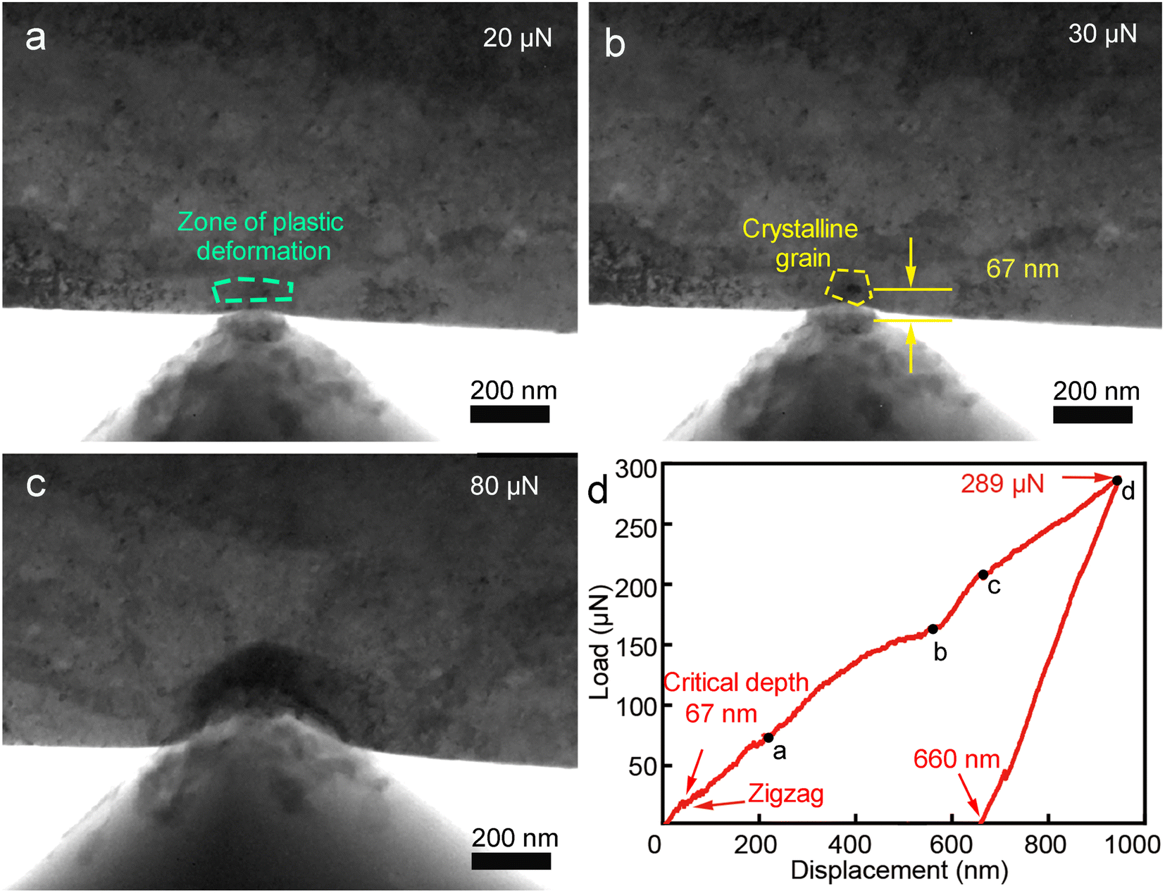 | ||
| Fig. 1 Snapshots of TEM images of the nanoindentation area at sequential loads of (a) 20, (b) 30, and (c) 80 μN; (d) load–displacement curve of nanoindentation. | ||
As stress levels escalated, the damaged area witnessed an initial onset of dislocation motion and the emergence of stacking faults. Subsequently, grain fracture took place. Stress during the sample loading process was meticulously calculated. As illustrated in Fig. 1(d), grain fracture occurred in monocrystalline nanoplate when the load reached 30 μN, corresponding to a displacement of 67 nm. In the realm of nanoindentation experiments, the equation employed to calculate the stress is as follows36
| Sp = P/Ac | (1) |
‘P’ represents the peak load, while ‘Ac’ denotes the projected area of contact. It is important to note that the indenter used in nanoindentation features a cube-corner tip, and the value of ‘Ac’ is explicitly expressed as37
 | (2) |
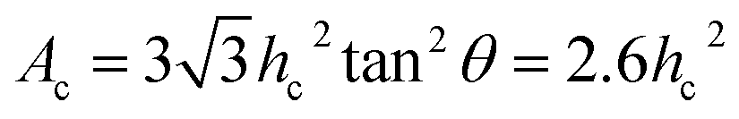
To further substantiate the above experimental results, a high-resolution observation of the damaged area was conducted. Fig. 2 presents an analysis of the damage structure of single-crystal copper nanoplates under different loads during the in situ nanoindentation process. As shown in Fig. 2(a), before indentation, the sample surface remained single-crystalline, with a 2 nm amorphous layer originating from the FIB processing damage. Moreover, the inset of Fig. 2 further illustrates that the sample presents a monocrystalline state before indentation. In Fig. 2(b), the crystal plane on the vertical surface is (220), indicating that the loading direction is 〈220〉 orientation. In Fig. 2(c), when a load of 20 μN was applied, upon magnification of the indented area, a high density of dislocations can be observed beneath the indentation. These dislocations are distributed within a semi-spherical three-dimensional plastic deformation zone, indicating severe plastic deformation in the region near the center of the indenter. This plastic deformation zone has also been observed in other metals and alloys, consistent with the traditional nanoindentation plasticity theories.38–40 Further magnification of the region near the indenter center revealed a significant number of stacking faults with a width of 3 to 4 atomic plane spacings (Fig. 2(d)). As the load increases to 30 μN, high-resolution characterization of the damaged surface, as shown in Fig. 2(e), revealed a larger grain on the upper right side of the indented area, as marked by the yellow dotted line. Further, the fast Fourier transform (FFT) pattern presents multiple sets of diffraction spots (inset of Fig. 2(e)). This suggests that at 30 μN, the damage mechanism in the indented area transitions from stacking faults to grain fragmentation. When the load reaches 80 μN, structural characterization of the damaged region, as shown in Fig. 2(f), reveals multiple fractured grains at the center of the indentation. The FFT pattern shows polycrystalline characteristics (inset of Fig. 2(f)). This indicates that with increasing stress, larger grains further undergo fragmentation and transform into smaller grains, namely, grain refinement.
 | ||
| Fig. 2 HRTEM images of the damage evolution process at sequential loads of (a and b) 0, (c and d) 20, (e) 30, and (f) 80 μN. The insets of (a), (e), and (f) show the respective FFT patterns. | ||
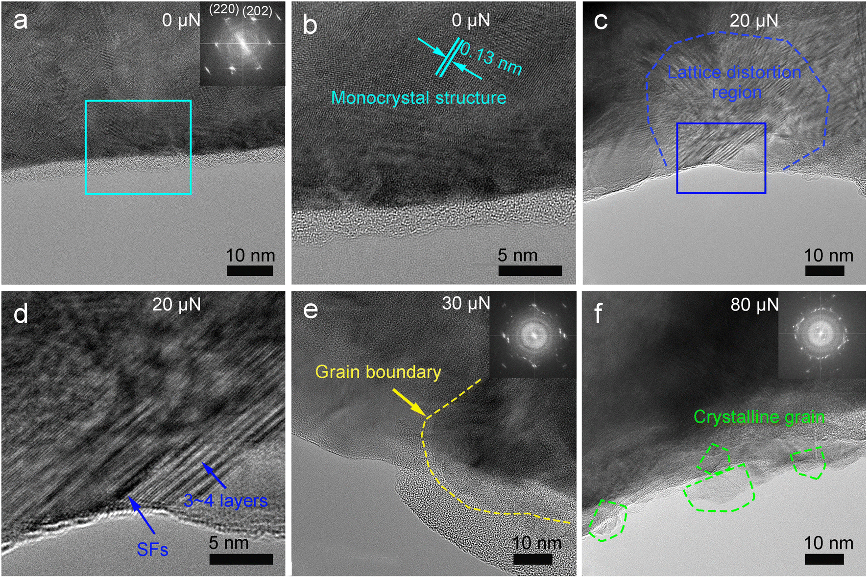
To validate the machining damage mechanism, three typical processing techniques, lapping, mechanical polishing, and chemical mechanical polishing, were conducted. Fig. 3 illustrates the surface quality and topographical characteristics after consolidated abrasive lapping, mechanical polishing, and CMP processes. As depicted in Fig. 3(a), after lapping, numerous intersecting scratches were evident, characterized by a relatively significant depth. Surface roughness measurements were conducted using a 3D optical profilometer. The surface roughness parameters, namely Ra (arithmetic mean height), Rq (root mean square height), and Rz (maximum height) were determined to be 16.42 nm, 21.01 nm, and 165.79 nm, respectively. These measurements were obtained over a scan area of 50 μm × 50 μm (Fig. 3(d)). Upon completion of polishing with ceria slurry, a remarkable reduction in the number and intensity of scratches was observed (Fig. 3(b)). Additionally, an assessment of the surface quality was carried out, revealing surface roughness of Ra, Rq, and Rz of 1.74 nm, 2.63 nm, and 28.79 nm, respectively. Afterward, utilizing an innovative polishing slurry, an exemplarily smooth copper surface was successfully obtained without scratches. The treated surface displayed an immaculate mirror-like smoothness, devoid of any indications of scratch-induced harm or corrosion marks. The surface roughness parameters for the polished copper, specifically Ra, Rq, and Rz, were measured to be 0.20 nm, 0.26 nm, and 1.65 nm, respectively, over a scanning area of 50 μm × 50 μm.
 | ||
| Fig. 3 Optical images of the copper wafer after (a) lapping with consolidated abrasive, (b) mechanical polishing with ceria slurry, and (c) polishing with a novel CMP slurry. Surface roughness and morphologies measured using a ZYGO profilometer after (d) lapping, (e) mechanical polishing, and (f) CMP. | ||
Directly observing surface damage provides compelling evidence for surface processing. TEM technique could be utilized to scrutinize sub-surface damage as well as surface defects.41,42Fig. 4 presents the TEM results for lapping with consolidated abrasive. In Fig. 4(a), the TEM investigation unveiled that the thickness of the lapping-induced damaged layer was 300 nm. Before lapping, the copper sample demonstrated a remarkably monocrystalline state, as visually depicted in the inset of Fig. 4(a). Nevertheless, following the lapping procedure, a transition from a monocrystalline pattern to a polycrystalline state was observed in Fig. 4(b), which indicates grain breakage happening during lapping. The damaged area was further analyzed to gain deeper insights into the damage types that arose from the lapping process. In the lower leftmost region of the damage site, monocrystal structural breakage occurred due to the presence of high abrasive stress. This resulted in the emergence of conspicuous moiré fringes and grain boundaries, as indicated by the green arrows and dotted line in Fig. 4(b). These fringes originate from the overlapping and intersection of two crystalline grains.43 Additionally, within the fractured crystal grains (Fig. 4(c)), regions of severe lattice distortion became apparent. Moving further into the interior of the damaged layer, as the abrasive stress diminishes, a distinct dislocation becomes discernible, clearly delineated by the yellow square (Fig. 4(d)). The inverse fast Fourier transform (IFFT) image, focusing on the region indicated by the yellow square in Fig. 4(b), unveils the presence of edge dislocations within the inner zone of the damaged layer.
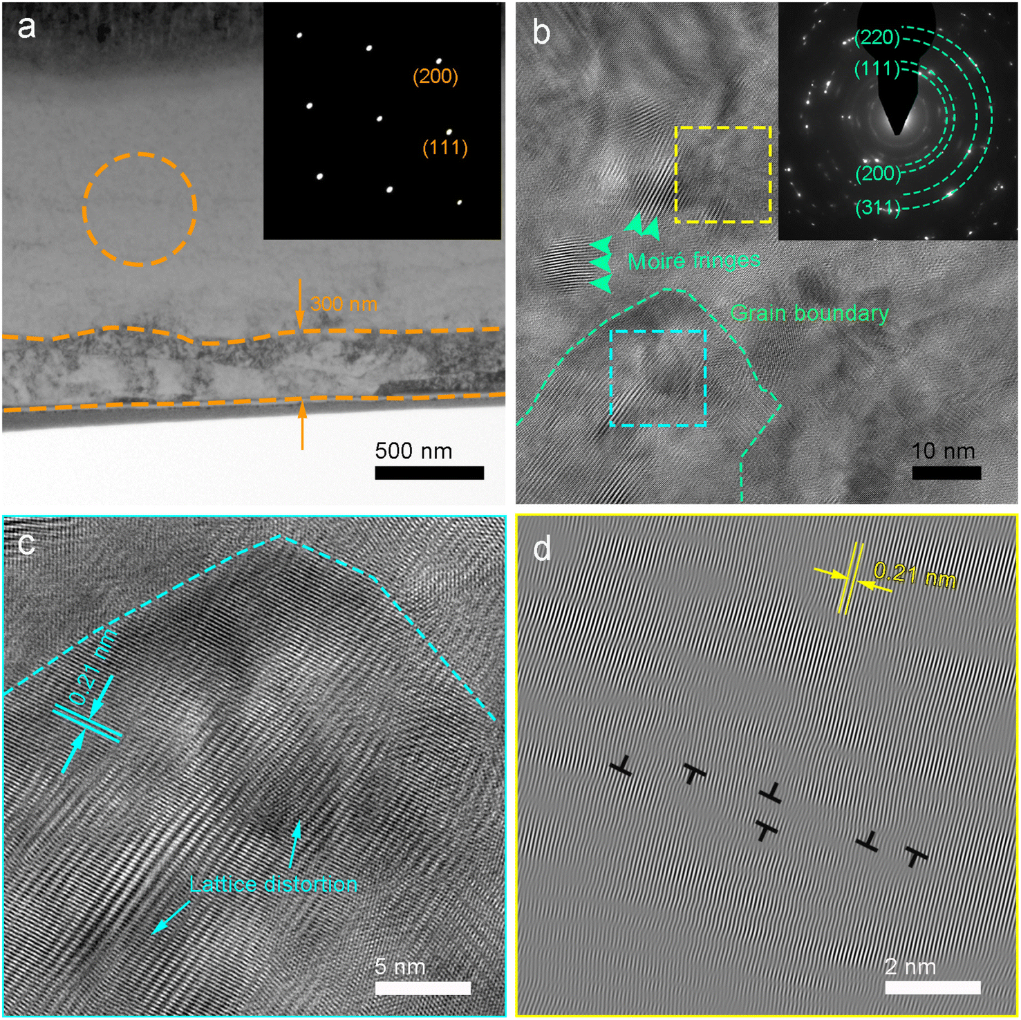 | ||
| Fig. 4 TEM characterization of copper subsurface after lapping. (a) A low magnification TEM image of subsurface damage, (b) an enlarged TEM image of the damaged area, (c and d) high-resolution TEM images obtained to visualize the damaged area, with distinct damage types corresponding to specific zones marked by cyan (c) and yellow (d) squares. The insets in (a) and (b) are their SAED patterns. | ||
In short, the damaged layer encompasses a variety of components, namely moiré fringes, grain boundaries, and edge dislocations. Within the outermost portion of the damage layer, the predominant form of damage consists of fractured grains. Nevertheless, by delving deeper into the damaged layer, defects assume a more significant role.
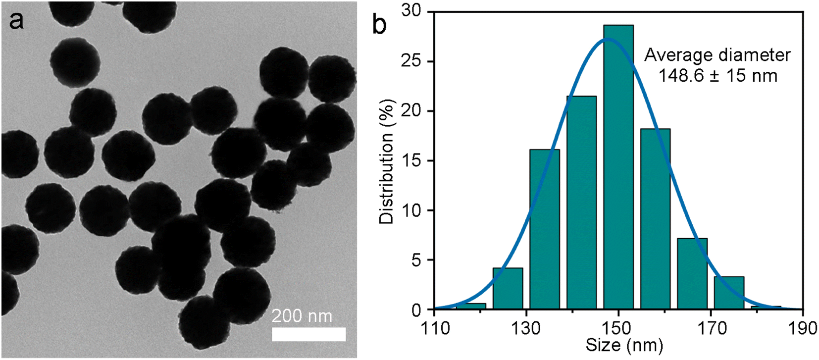
Mechanical polishing is a precision polishing technology, that mainly relies on very fine polishing powder or polishing slurry lapping, rolling action, removing a layer of extremely thin material on the surface of the sample until the required smoothness is reached.44Fig. 5(a) shows the TEM image of ceria abrasive particles, indicating uniform dispersion of ceria. Particle size statistics revealed a normal distribution for ceria particles, with an average abrasive diameter of 148 nm (Fig. 5(b)).
 | ||
| Fig. 5 (a) TEM image and (b) particle size distribution of CeO2 abrasives. | ||
After performing mechanical polishing, the investigation of subsurface damage at the atomic scale was performed using TEM. A low magnification TEM image presents a cross-sectional perspective of a mechanically polished surface, demonstrating a measured damage layer thickness of 33 nanometers (Fig. 6(a)). Additionally, the polished surface retained its monocrystalline structure (inset in Fig. 6(c)). Furthermore, the structure of the damage layer was observed. As depicted in Fig. 6(b), sporadic defects, including twin structures and stacking faults, were evident in the inner region. Notably, the width of these twin structures was measured at approximately 4.23 nm. The formation of an ordered periodic structure, as demonstrated in Fig. 6(d), was initiated through the alignment of the AB-type structure of two (111) planes within the superficial region, resulting from the vast stacking fault structure. In short, as the depth of the damage layer increases, the stress experienced by the sample gradually decreases, and the defect density also decreases accordingly.
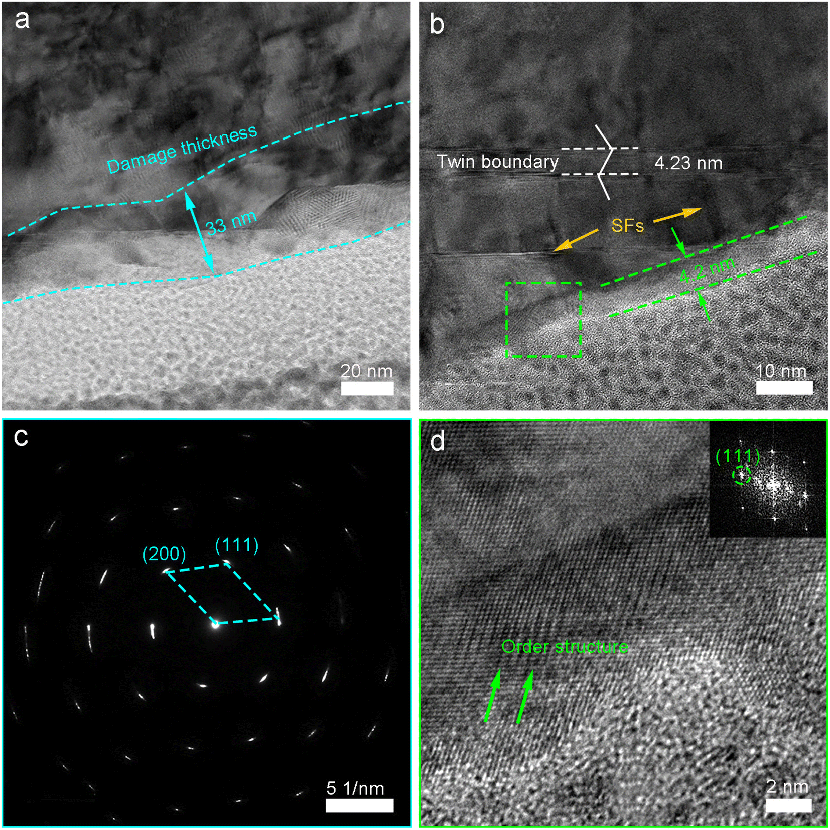 | ||
| Fig. 6 (a) TEM characterization of the copper subsurface after mechanical polishing. (a) The low magnification TEM image of subsurface damage, (b) enlarged TEM image of the damaged area, (c) a SAED pattern of (a), and (d) HRTEM image of the green square in (b). | ||
After conducting CMP, a TEM cross-section sample was meticulously prepared by employing FIB technology, enabling an in-depth analysis of the damage incurred during the polishing process. As illustrated in Fig. 7(a), a protective layer was strategically employed to shield the damaged layer from the potentially deleterious effects of the ion beam. Within the subsurface realm of the copper sample, a remarkable preservation of its single-crystal state was observed, as vividly presented in the inset of Fig. 7(b). Subsequently, upon scrutinizing the damaged area with precision, it was determined that the thickness of the damaged layer on the polished copper wafer was measured at a mere 3.1 nm, as depicted in Fig. 7(b). Furthermore, diverse damaged areas at distinct locations were meticulously characterized, revealing the presence of stacking faults composed of single-layer atoms, as impeccably exemplified in Fig. 7(c). Fig. 7(d) offers valuable insights into the core structure of twins, each measuring approximately 2 nm in length. To comprehensively assess the stress introduced by the polishing process, a microstrain analysis was conducted on the high-resolution TEM image employing geometric phase analysis (GPA) techniques, as elaborated in prior studies.45,46 The strain maps meticulously charted the variations along [11![[1 with combining macron]](https://www.rsc.org/images/entities/char_0031_0304.gif) ] and [200] directions (Fig. 7(b)). Within these strain maps, regions colored blue denoted compressive strain, whereas red and green regions signified tensile strain and an absence of strain, respectively. Notably, a conspicuous variation in strain was particularly pronounced along the [11] direction, whereas the [200] direction exhibited a notable lack of substantial stress distribution (εxx in Fig. 7(e)). It is worth mentioning the presence of a considerable degree of compressive stress between the (11) planes (εyy in Fig. 7(f)). The findings highlight that the CMP technology generates processing stress, notably manifesting in a direction parallel to the wafer's surface.
] and [200] directions (Fig. 7(b)). Within these strain maps, regions colored blue denoted compressive strain, whereas red and green regions signified tensile strain and an absence of strain, respectively. Notably, a conspicuous variation in strain was particularly pronounced along the [11] direction, whereas the [200] direction exhibited a notable lack of substantial stress distribution (εxx in Fig. 7(e)). It is worth mentioning the presence of a considerable degree of compressive stress between the (11) planes (εyy in Fig. 7(f)). The findings highlight that the CMP technology generates processing stress, notably manifesting in a direction parallel to the wafer's surface.
 | ||
| Fig. 7 TEM characterization of the copper subsurface after chemical mechanical polishing. (a) A low-magnification cross-sectional TEM image of subsurface and surface damage, (b) enlarged TEM image of the damaged area, (c and d) HRTEM images of different structure defects in different damaged regions, strains maps (e) εxx and (f) εyy obtained by GPA. The inset in (b) shows the SAED pattern of (b). | ||
Discussion
Nanoindentation is a common technology that is used to study the deformation mechanisms. Since Nix and Gao et al.47 proposed the geometric necessity dislocation (GND) based on single crystal metal materials in 1998, the study of the universal model and nanoindentation mechanism has attracted extensive attention. Nanoindentation offers significant potential in unraveling the intricate atomic rearrangements occurring under stress. This potential spans from comprehending defect evolution within small material volumes to tracking the movement and formation of specific imperfections, such as lattice dislocations or shear bands.48 In high-precision machining, the formation of subsurface and surface damage in workpieces is primarily caused by the interaction between the cutting edge on the trailing cutting face and the workpiece, involving contact, compression, and shearing actions.49 Although experimental conditions (e.g., the stress level, indenter shape, grain morphology of the polishing agent, etc.) were different during high-precision machining, researchers typically widely adopt the slip-line field theory to establish cutting models and calculate cutting forces.50 Meanwhile, scholars have observed that in high-precision machining processes, the normal force plays a crucial role in influencing material plastic deformation and damage formation. Hence, nano-indentation experiments can also be employed to investigate the formation and evolution of damage during the mechanical machining process.In high-precision machining, the processing precision of consolidated abrasive lapping, mechanical polishing, and chemical mechanical polishing gradually improves. As a result, the cutting depth and load generated by these processing techniques decrease step by step, leading to significantly different surface damage, damage depth, damage structure, and damage forms.51 During the lapping process of the consolidated abrasive, the stress on the copper surface exceeds the GPa level.18 When an external load is applied to a sample, in the actual crystal, the dislocation's slip encounters numerous resistances. As a dislocation with a Burgers vector moves within the crystal, it transitions from one symmetric position to the other symmetric position. When the dislocation is at these symmetric positions, it is in equilibrium, with lower energy. However, between the symmetric positions, the energy increases, which creates resistance to the dislocation's movement. Therefore, as the dislocation moves, a force is needed to overcome the lattice resistance and surpass the energy barrier, and this force is known as the Peierls force. It represents the shear stress required for the onset of dislocation slip, and the equation for Peierls force is as follows,52
 | (3) |
 | (4) |
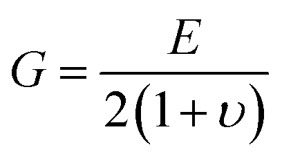
The lattice constant of single crystal copper is 0.361 nm, and its elastic modulus ‘E’ in the 〈110〉 crystal direction within the {111} plane is 137 GPa.54 The corresponding Poisson's ratio ‘ν’ is 0.33. The ratio between the slip plane ‘h’ and the Burgers vector ‘b’ for the {111}〈110〉 slip system is 1.41.55 According to eqn (3) and (4), the Peierls stress is calculated to be 0.28 MPa. Consequently, before the emergence of new grains, dislocation motion must have occurred. Furthermore, in order to confirm that crystal slip processes occur before grain fragmentation, a further calculation of the critical shear stress was conducted. The critical shear stress is the minimum shear stress required to initiate slip within a slip system. According to existing literature, the critical shear stress for the activation of {111}〈110〉 slip system is reported to be 170 MPa,56 a value significantly lower than the average stress experienced in the indentation region. In summary, during the single-crystal nanoindentation process, dislocation motion occurs first, leading to the formation of stacking faults and subsequently resulting in the fracture of crystalline grains.
Cutting depth is a crucial parameter that affects the quality of machining surfaces and the structure of the damage layer. According to the above experimental results, a relationship between the cutting depth and the damage generated during precision machining is established. The cutting depth for different processes was calculated, with specific details explained in the ESI.† The surface damage layer produced by the lapping process contains defects such as lattice distortions, broken grains, and edge dislocations. The surface of the sample was subjected to higher lapping stress, resulting in more severe damage, with a large number of broken grains in the damaged layer. The subsurface, on the other hand, experiences lower lapping stress, leading to relatively lower damage, characterized by the presence of numerous crystal defects such as high-density stacking faults in the damaged layer (Fig. 8). During the mechanical polishing process, the stress on the copper surface exceeds the MPa level.19 The damaged layer contains a significant amount of dislocation structures, and the density of dislocations decreases with increasing depth of the damaged layer. Moreover, in chemical mechanical polishing, copper atoms are collectively removed under mechanical and chemical action, forming micro-stacking faults composed of only a few atomic layers on the surface (Fig. 8). In high-precision machining, severe damage caused by broken grains significantly affects the surface quality and material mechanical properties of copper devices. It is essential to avoid such damage in practical machining processes. The in situ nanoindentation technique, employed in this study, determines the critical depth required for grain breakage to be 67 nm.
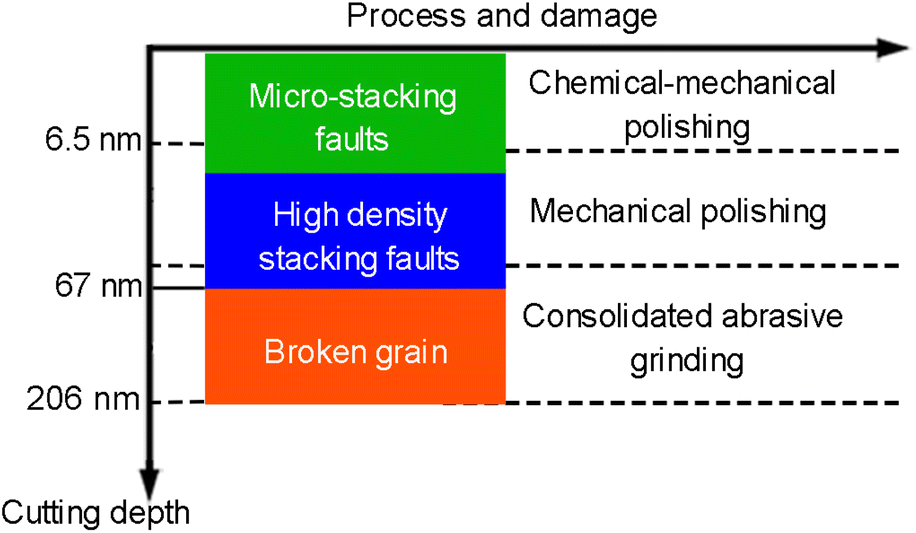 | ||
| Fig. 8 Diagram of damage evolution under different process conditions. | ||
Conclusions
In summary, in situ TEM nanoindentation was employed to investigate the machining damage mechanism. TEM results showed that damages originate from dislocations, evolving to stack faults, and then causing broken crystallites. Moreover, the critical depth required for the transformation of defects such as dislocations and stacking faults into fractured grains was 67 nm, corresponding to an indentation stress of 2.57 GPa. The surface quality and damaged structure of the copper surface were investigated separately using three different techniques, namely consolidated abrasive lapping, mechanical polishing, and chemical mechanical polishing based on the differences in processing precision. Results indicate that the surface roughness after processing with lapping, mechanical polishing, and chemical mechanical polishing techniques were 16.42 nm, 1.74 nm, and 0.20 nm, respectively, within a measured area of 50 μm × 50 μm. Through TEM analysis, we revealed that the structure within the subsurface damage evolves from fractured grain structures to dislocation and micro-twin structures. This research can provide a theoretical foundation for controlling damage in high-precision machining.Author contributions
Dong Wang: investigation, formal analysis, data curation. Zhenyu Zhang: funding acquisition, visualization, project administration, conceptualization, supervision. Dongdong Liu: investigation, formal analysis. Xingqiao Deng: formal analysis, visualization, data curation. Chunjing Shi: investigation, formal analysis. Yang Gu: formal analysis, data curation. Xiuqing Liu: formal analysis, validation. Xiaoyu Liu: investigation, formal analysis. Wei Wen investigation, formal analysis.Conflicts of interest
The authors declare that they have no known competing financial interests or personal relationships that could have appeared to influence the work reported in this paper.Acknowledgements
This work was supported by the National Key Research and Development Program of China (2018YFA0703400), and the Changjiang Scholars Program of the Chinese Ministry of Education.References
- T. H. Fang, W. L. Li, N. R. Tao and K. Lu, Science, 2011, 331, 1587–1590 CrossRef CAS PubMed.
- Y. F. Shen, L. Lu, Q. H. Lu, Z. H. Jin and K. Lu, Scr. Mater., 2005, 52, 989–994 CrossRef CAS.
- Y. T. Zhu and X. L. Wu, Mater. Today Nano, 2018, 2, 15–20 CrossRef.
- T. Kvackaj, A. Kovacova, R. Kocisko, J. Bidulska, L. Lityńska-Dobrzyńska, P. Jenei and J. Gubicza, Mater. Charact., 2017, 134, 246–252 CrossRef CAS.
- L. Lu, Y. Shen, X. Chen, L. Qian and K. Lu, Science, 2004, 304, 422–426 CrossRef CAS PubMed.
- S. J. Kim, Y. I. Kim, B. Lamichhane, Y. H. Kim, Y. Lee, C. R. Cho, M. Cheon, J. C. Kim, H. Y. Jeong, T. Ha, J. Kim, Y. H. Lee, S. G. Kim, Y. M. Kim and S. Y. Jeong, Nature, 2022, 603, 434–438 CrossRef CAS PubMed.
- X. Zeng, P. He, M. Hu, W. Zhao, H. Chen, L. Liu, J. Sun and J. Yang, Nanoscale, 2022, 14, 16003–16032 RSC.
- Q. Mao, Y. Zhang, Y. Guo and Y. Zhao, Commun. Mater., 2021, 2, 46 CrossRef CAS.
- K. H. Z. Gahr, Wear, 1981, 74, 353–373 CrossRef CAS.
- L. Lu, R. Schwaiger, Z. W. Shan, M. Dao, K. Lu and S. Suresh, Acta Mater., 2005, 53, 2169–2179 CrossRef CAS.
- B. Goh and J. Choi, Surf. Interfaces, 2021, 26, 101388 CrossRef CAS.
- X. Meng, W. Wu, B. Liao and H. Dai, Ceram. Int., 2022, 48, 17034–17045 CrossRef CAS.
- S. J. Zhang, S. To, S. J. Wang and Z. W. Zhu, Int. J. Mach. Tools Manuf., 2015, 91, 76–95 CrossRef.
- S. Yin, P. Cavaliere, B. Aldwell, R. Jenkins, H. Liao, W. Li and R. Lupoi, Addit. Manuf., 2018, 21, 628–650 CAS.
- W. K. Neo, A. S. Kumar and M. Rahman, Int. J. Adv. Manuf. Technol., 2012, 63, 465–480 CrossRef.
- S. Agarwal and P. V. Rao, Int. J. Mach. Tools Manuf., 2008, 48, 698–710 CrossRef.
- S. Sharma and A. Meena, J. Manuf. Process., 2020, 50, 345–365 CrossRef.
- W. L. Li, N. R. Tao and K. Lu, Scr. Mater., 2008, 59, 546–549 CrossRef CAS.
- X. Han, Z. Jin, Q. Mu, Y. Yan and P. Zhou, J. Mater. Process. Technol., 2022, 307, 117689 CrossRef CAS.
- N. Ikawa, S. Shimada and H. Tanaka, Nanotechnology, 1992, 3, 6–9 CrossRef.
- Z. Kou, Y. Wan, Y. Cai, X. Liang and Z. Liu, Procedia Manuf., 2015, 1, 501–511 CrossRef.
- Q. Wang, Q. Bai, J. Chen, Y. Sun, Y. Guo and Y. Liang, Appl. Surf. Sci., 2015, 344, 38–46 CrossRef CAS.
- D. Ulutan and T. Ozel, Int. J. Mach. Tools Manuf., 2011, 51, 250–280 CrossRef.
- H. Huang and Y. C. Liu, Int. J. Mach. Tools Manuf., 2003, 43, 811–823 CrossRef.
- O. Rodríguez de la Fuente, J. A. Zimmerman, M. A. González, J. de la Figuera, J. C. Hamilton, W. W. Pai and J. M. Rojo, Phys. Rev. Lett., 2002, 88, 036101 CrossRef.
- T. Inamura, N. Takezawa, K. Yamada and K. Shibuya, CIRP Ann., 2006, 55, 51–54 CrossRef.
- T. Voisin, M. D. Grapes, T. T. Li, M. K. Santala, Y. Zhang, J. P. Ligda, N. J. Lorenzo, B. E. Schuster, G. H. Campbell and T. P. Weihs, Mater. Today, 2020, 33, 10–16 CrossRef CAS.
- D. Kiener and A. M. Minor, Acta Mater., 2011, 59, 1328–1337 CrossRef CAS.
- M. Efe, B. Gwalani, J. Tao, M. Song, T. C. Kaspar, A. Devaraj and A. Rohatgi, Appl. Surf. Sci., 2021, 562, 150132 CrossRef CAS.
- P. Ranjan, A. Owhal, D. Chakrabarti, S. U. Belgamwar, T. Roy and R. Balasubramaniam, Mater. Today Commun., 2022, 32, 103980 CrossRef CAS.
- J. J. Zhang, T. Sun, Y. D. Yan, Y. C. Liang and S. Dong, Appl. Surf. Sci., 2008, 254, 4774–4779 CrossRef CAS.
- Y. Gao and H. M. Urbassek, Appl. Surf. Sci., 2014, 317, 6–10 CrossRef CAS.
- C. Liu, Z. Zhuang, J. Chen, W. S. Yip and S. To, Surf. Interfaces, 2023, 40, 103126 CrossRef CAS.
- Q. Wang, C. Zhang, M. Wu and J. Chen, China Mech. Eng., 2019, 30, 1959–1966 Search PubMed.
- J. H. Lee, I. Kim, D. M. Hulbert, D. Jiang, A. K. Mukherjee, X. Zhang and H. Wang, Acta Mater., 2010, 58, 4891–4899 CrossRef CAS.
- R. Saha and W. D. Nix, Acta Mater., 2002, 50, 23–38 CrossRef CAS.
- D. Liu, Z. Zhang, L. Chen, D. Wang, J. Cui, K. Chang and D. Guo, Nanoscale, 2021, 13, 7169–7175 RSC.
- Y. L. Chiu and A. H. W. Ngan, Acta Mater., 2002, 50, 2677–2691 CrossRef CAS.
- Z.-Y. Nie, Y. Sato, S. Ogata, M. J. Duarte, G. Dehm, J. Li, E. Ma, D.-G. Xie and Z.-W. Shan, Acta Mater., 2022, 232, 117944 CrossRef CAS.
- A. Hosseinzadeh, A. Radi, J. Richter, T. Wegener, S. V. Sajadifar, T. Niendorf and G. G. Yapici, J. Manuf. Process., 2021, 68, 788–795 CrossRef.
- T. W. Pfeifer, J. A. Tomko, E. Hoglund, E. A. Scott, K. Hattar, K. Huynh, M. Liao, M. Goorsky and P. E. Hopkins, J. Appl. Phys., 2022, 132(7), 075112 CrossRef CAS.
- A. L. Clauser, R. Giulian, Z. D. McClure, K. O. Sarfo, C. Ophus, J. Ciston, L. Árnadóttir and M. K. Santala, Scr. Mater., 2020, 188, 44–49 CrossRef CAS.
- C. Jin, E. C. Regan, A. Yan, M. Iqbal Bakti Utama, D. Wang, S. Zhao, Y. Qin, S. Yang, Z. Zheng, S. Shi, K. Watanabe, T. Taniguchi, S. Tongay, A. Zettl and F. Wang, Nature, 2019, 567, 76–80 CrossRef CAS.
- A. Kubota, S. Nagae and S. Motoyama, Diamond Relat. Mater., 2020, 101, 107644 CrossRef CAS.
- Z. Chen, F. Li, Q. Huang, F. Liu, F. Wang, S. P. Ringer, H. Luo, S. Zhang, L.-Q. Chen and X. Liao, Sci. Adv., 2020, 6, eabc7156 CrossRef CAS.
- J. J. P. Peters, R. Beanland, M. Alexe, J. W. Cockburn, D. G. Revin, S. Zhang and A. M. Sánchez, Ultramicroscopy, 2015, 157, 91–97 CrossRef CAS PubMed.
- W. D. Nix and H. Gao, J. Mech. Phys. Solids, 1998, 46, 411–425 CrossRef CAS.
- C. A. Schuh, Mater. Today, 2006, 9, 32–40 CrossRef CAS.
- I. Inasaki, CIRP Ann., 1987, 36, 463–471 CrossRef CAS.
- N. Fang, J. Mech. Phys. Solids, 2003, 51, 715–742 CrossRef.
- H. Zhou, W. Jiang, J. Ji, X. Ren, Z. Zhu and C. Zhang, Int. J. Adv. Manuf. Technol., 2022, 119, 855–864 CrossRef.
- Y. Kamimura, K. Edagawa, A. M. Iskandarov, M. Osawa, Y. Umeno and S. Takeuchi, Acta Mater., 2018, 148, 355–362 CrossRef CAS.
- M. Domingo-Espin, J. M. Puigoriol-Forcada, A.-A. Garcia-Granada, J. Llumà, S. Borros and G. Reyes, Mater. Des., 2015, 83, 670–677 CrossRef CAS.
- H. Liang, C. H. Woo, H.-C. Huang, A. H. W. Ngan and T. Yu, Comput. Model. Eng. Sci., 2004, 6, 105–114 Search PubMed.
- Y. Kamimura, K. Edagawa and S. Takeuchi, Acta Mater., 2013, 61, 294–309 CrossRef CAS.
- M. J. Pfetzing, S. Brinckmann, S. R. Dey, F. Otto, A. Hartmaier and G. Eggeler, Mater. Sci.Eng. Technol., 2011, 42, 219–223 Search PubMed.
Footnote |
| † Electronic supplementary information (ESI) available. See DOI: https://doi.org/10.1039/d3na00960b |
| This journal is © The Royal Society of Chemistry 2024 |