
 Open Access Article
 This Open Access Article is licensed under a Creative Commons Attribution-Non Commercial 3.0 Unported Licence
Role of oxygen functional groups and attachment of Au nanoparticles on graphene oxide sheets for improved photodetection performance†
Ningthoujam Somorjit
Singh
 a,
Abdul Kaium
Mia
a and
P. K.
Giri
*ab
a,
Abdul Kaium
Mia
a and
P. K.
Giri
*ab
aCentre for Nanotechnology, Indian Institute of Technology Guwahati, Guwahati 781039, India. E-mail: giri@iitg.ac.in
bDepartment of Physics, Indian Institute of Technology Guwahati, Guwahati 781039, India
First published on 15th March 2024
Abstract
Integrating low-dimensional graphene oxide (GO) with conventional Si technology offers innovative strategies for developing ultrafast wideband photodetectors. In this study, we synthesized GO and explored its potential application in broadband photodetection alongside silicon heterostructures. The as-synthesized GO contains various oxygen functional groups, as evidenced by X-ray photoelectron and Fourier transform infrared spectroscopy. These functional groups contribute to increased photo absorption, enhancing photodetection performance. The systematic reduction of these functional groups from the GO surface via thermal annealing decreases photo absorption and consequently lowers the photocurrent. This reduction diminishes photo absorption and amplifies the dark current by approximately 25 times, from 20 nA to 496 nA. This dark current increase is attributed to the electron mobility following the reduction of functional groups. However, attaching plasmonic gold nanoparticles (Au NPs) to the GO surface enhances UV-Vis absorption in the visible region, enabling broadband detection. The even distribution of attached Au NPs on the GO surface is confirmed through field emission transmission electron microscopy. While thermal annealing of GO diminishes the responsivity from 4.6 A W−1 to 3.0 A W−1, the attachment of Au NPs augments the responsivity by more than two-fold, reaching 10.0 A W−1. Thus, it highlights the importance of rich oxygen functional groups in GO and the attachment of Au NPs to achieve more efficient photo-sensing properties.
1. Introduction
Graphite oxide, first synthesized around 164 years ago and gaining popularity after the discovery of graphene in 2004,1 can be exfoliated to produce graphene oxide (GO). GO is a two-dimensional material composed of oxygen functional groups, such as hydroxyl (–OH), carboxyl (–COOH), carbonyl (C![[double bond, length as m-dash]](https://www.rsc.org/images/entities/char_e001.gif) O), ether (C–O–C), and epoxy (O–CO),2 along with carbon atoms (sp2 and sp3). Pristine graphene has limited potential for use as an effective photodetector device due to its high transparency,3 lack of a band gap, and rapid carrier recombination. These limitations are overcome by oxidizing graphene to form GO/RGO, creating structural flaws that act as charge carrier trappers. The concentration of oxygen functional groups can alter the bandgap of GO (2.9 eV) and RGO (1.1 eV to 1.9 eV).4 GO-based photodetectors detect a broad spectrum of wavelengths from infrared to ultraviolet; structural defects and attached functional groups on GO enhance the photodetector's performance.5 Due to its unique features, research communities are interested in GO for various sensing applications.
O), ether (C–O–C), and epoxy (O–CO),2 along with carbon atoms (sp2 and sp3). Pristine graphene has limited potential for use as an effective photodetector device due to its high transparency,3 lack of a band gap, and rapid carrier recombination. These limitations are overcome by oxidizing graphene to form GO/RGO, creating structural flaws that act as charge carrier trappers. The concentration of oxygen functional groups can alter the bandgap of GO (2.9 eV) and RGO (1.1 eV to 1.9 eV).4 GO-based photodetectors detect a broad spectrum of wavelengths from infrared to ultraviolet; structural defects and attached functional groups on GO enhance the photodetector's performance.5 Due to its unique features, research communities are interested in GO for various sensing applications.
Photodetectors find wide applications across various industries, such as night surveillance, self-driving automobiles, military applications, remote control devices, etc.3,4,6–8 However, the existing semiconductor-based photodetector technology has drawbacks, including high cost, low operating temperature, toxicity, opacity, complicated manufacturing technology, and scarcity.8 Some of the reported literature on GO-based photodetectors is discussed below and shown in Table 1. Yang Cao et al.9 created an ultra-board band photodetector using a self-assembling RGO–silicon nanowires array heterojunction. With an excitation laser of 532 nm and a bias voltage of 1 V, they showed a responsivity (R) of 0.33 mA W−1 with rise (τrise) and fall (τfall) times of 10.6 and 6.7 s, respectively. Sin Ki Lai et al.10 synthesized GO and fabricated a GO–metal photodetector using hydrothermal. With the irradiation of 375 nm laser and a bias voltage of 1 V, the photodetector's R measured as 23.6 mA W−1, and the τrise and τfall time of 105 ms. The photocurrent (Iph) of graphene/Si heterojunctions are investigated by Xiaohong An et al.11 The τrise and τfall are 1.2 and 3 ms, respectively, and they showed that the R is tunable up to 435 mA W−1. The RGO-based photodetector having an R of 0.12 A W−1 and the τrise and τfall as 30 and 35 minutes, respectively, is demonstrated by Chitara et al.12
| Active material | Excitation wavelength (nm) | Responsivity (A W−1) | Response time (s) | Reference | |
|---|---|---|---|---|---|
| Rise time | Decay time | ||||
| RGO/n-Si | 600 | 1.52 | 2 | 2 | 8 |
| RGO/n-Si | 405 | 0.05 | — | — | 38 |
| GO/SiNW | 532 | 0.033 | 10.6 | 6.7 | 9 |
| GO | 375 | 0.0236 | 0.105 | 0.105 | 10 |
| Graphene/Si | 488 | 0.435 | 0.0012 | 0.003 | 11 |
| GO | 455 | 0.0958 | 5.65 | 6.97 | 39 |
| Graphene/GaAs | 532 | 0.231 | 85 × 10−6 | 118 × 10−6 | 40 |
| WS2-QDs/RGO | 405 | 0.12 | 1.97 | 2.39 | 34 |
| RGO femtogel | 465 | 0.73 | — | — | 41 |
| RGO–ZnO | 365 | 3.24 | 17.9 | 46.6 | 42 |
| RGO film | 360 | 0.12 | 1.8 ×10³ | 2.1 × 10³ | 12 |
| RGO film | 530 | 0.55 | 240 | 300 | 43 |
| GO/p-Si | 405 | 4.64 | 8.2 × 10⁻⁶ | 295 × 10−6 | Our work |
| Au–GO/p-Si | 405 | 10 | 24 × 10−6 | 208 × 10−6 | Our work |
GO and RGO are rarely used for practical photodetector applications, even though the materials offer several highly significant properties for optoelectronic applications.3 As indicated in Table 1, GO/RGO-based photodetectors detect a wide range of wavelengths from UV to infrared. However, the reported responsivity is relatively low compared to the conventional semiconductor-based photodetectors. In our work, we have surpassed the performance parameters of various reported devices in terms of very high on/off ratio (6465), responsivity (4.64 A W−1), and response time (τrise: 8.21 μs and τfall: 295.15 μs) of untreated GO (GO-RT). We also studied the effect of annealing of GO at temperatures of 85 °C, 120 °C, and 230 °C to tune the oxygen functional groups. Photodetectors based on different temperature annealed GO (GO-85 for 85 °C, GO-120 for 120 °C, and GO-230 for 230 °C) are fabricated on p-type-doped silicon (p-Si) substrates using interdigitated electrodes (IDE). Further, we enhanced the photo-sensing properties of GO-RT by decorating Au nanoparticles (NPs) on it (AuGO). It is well known that Au NPs show surface plasmon resonance-induced absorption peak in the visible range, which is size dependent, and thus, the combination of Au NPs with GO may give rise to higher photo response in the UV-visible range, as GO is more sensitive towards UV region. Thus, a systematic study of the effect of Au NPS on GO-based photodetectors is carried out in this work.
2. Experimental details
2.1. Synthesis of graphene oxide, Au nanoparticles, and anneal graphene oxide
Graphene oxide (GO) is exfoliated from the graphite oxide, which is synthesized using the modified Hummers' method; the details of the synthesis process are reported in our previous work.13 In brief, 0.5 g of graphite flakes (Asbury Carbon) is mixed with 4 g of potassium permanganate (KMnO4) and 0.5 g of sodium nitrate (NaNO3) in a conical flask. Subsequently, 100 ml of sulphuric acid (98% conc. H2SO4) is poured drop by drop into the flask and mixed in the solution. The solution is on the hot plate for 14 hours at 60 °C. Thus, highly oxidized graphite oxide is synthesized. The solution is diluted by de-ionized water; the unwanted metal impurities are removed and dried in a vacuum oven to produce a solid graphite oxide. Finally, graphite oxide is exfoliated into GO using the mild heating technique. This process gives rise to ultra-large area GO sheets. Au NPs are synthesized through a commonly employed chemical process involving gold chloride and trisodium citrate. KMnO4, NaNO3, and H2SO4 are procured from Merck.2.2. Fabrication of inter digitated electrode (IDE)
IDE patterns with a 10 μm channel width are fabricated on a p-type silicon using UV lithography. The substrate undergoes a thorough cleaning process involving sequential treatments with piranha solution, ethanol, and acetone. Subsequently, it is dried using N2 and heated at 85 °C in a hot oven for 2 hours. The substrate is deposited a positive photoresist (MicroChemicals GmbH: S1813) using a spin coater (Apex equipment: spinNXG-M1) at 3500 RPM for 60 seconds. The IDE pattern is designed using K-layout software, and the program is executed through the system software (DilaseSoft). A thermal evaporator deposits the metal electrode (aluminium) on the substrate. The IDE fingers maintain a width and gap of 10 μm, with a total of 10 finger pairs, as shown in Fig. S1.† Additionally, the substrate features two metal pads, each measuring (2.5 × 1) mm in width and length, serving as adequate points for probing the electrodes' electrical tips.GO-based photodetector devices are made on the pre-fabricated inter-digitated electrode (IDE) pattern on the p-Si substrate by drop-casting the GO solution. This fabrication involves drop-casting a 5 μl exfoliated GO solution (water) onto the IDE pattern using a micropipette (Accupipet). The deposited solution is left to dry inside a desiccator overnight at room temperature (RT); this device is named GO-RT. Subsequently, GO-85, GO-120, and GO-230 devices are prepared through thermal treatment of GO at temperatures of 85 °C, 120 °C, and 230 °C, respectively. These devices undergo annealing for 3 hours at their respective temperatures inside a hot air oven before cooling back to RT for further analysis.
3. Characterization techniques
The field emission scanning electron microscope (FESEM) (JEOL, JSM-7610F) is used to investigate the morphology of GO and the IDE pattern on the p-Si substrate. The structural properties of as-prepared GO and thermally annealed GO are measured using an XRD (Rigaku, RINT 2500 TTRAX-III) and Raman spectroscopy (Horiba, LabRam HR). The functional groups attached to the GO-based materials are examined using an X-ray photoelectron spectroscopy (XPS) (PHI X-tool, ULVAC-PHI INC) and the transmittance mode of Fourier transform infrared (FTIR) spectroscopy (PerkinElmer, Spectrum BX). The photoluminescence (PL) of the GO solution is measured using a fluorimeter (Horiba, Fluromax-4) at 360 nm excitation.The photo-sensing properties of GO-based devices are measured using a customized I–V characterization setup, an assembly of various components such as a microprobe station (ECOPIA, EPS-500), source-measure unit (Keithley 4200), 405 nm diode laser (CNI Laser), and pulse generator (Scientific). Micro-tips are probed on the metal pads of the device. The laser source, with variable power, is used to measure power-dependent characteristics. Further, a pulse generator is connected to the laser source for measuring the response time.
4. Results and discussion
4.1. Material characterizations
The material characterizations of GO and thermally annealed GO are well explained in our previous reports.13 Both GO and annealed GO underwent characterization using XRD, Raman spectroscopy, XPS, FTIR, UV absorbance, and PL. The XRD (Fig. 1a) and Raman spectra were employed for structural analysis of the GO and annealed GO samples. A significant peak at 10.9° corresponds to the (002) plane of untreated GO (GO-RT), while a broad peak in the range ∼10° to 21° indicates the presence of rich oxygen functional groups in the GO-RT.2,14 In the thermally annealed GO at 85 °C (GO-85), the intensity of the oxidized peak at 10.9° decreases, while a distinct peak at 25.6° emerges, illustrating the transition of GO to reduced graphene oxide (RGO). The GO-85 process partially eliminates loosely attached oxygen groups, such as –OH, C–O, and O–CO, after the heat treatment at 85 °C for 3 hours.
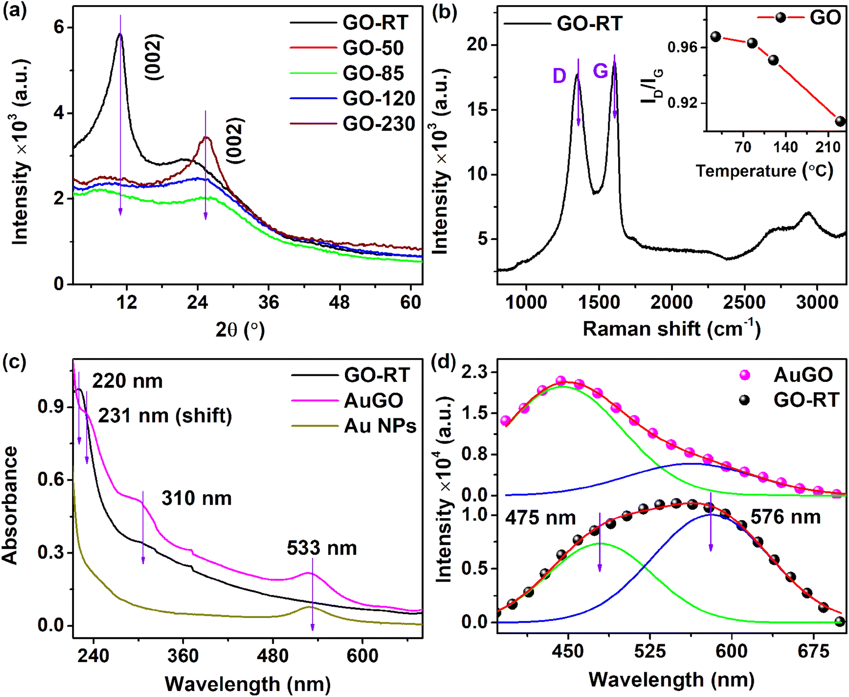 | ||
| Fig. 1 (a) XRD pattern of GO samples before and after annealing, and (b) Raman spectra of GO-RT (inset: ID/IG ratio for different temperature annealed GO); (c) UV-visible absorption spectra of AuGO, GO-RT, and Au NPs; and (d) PL spectra of GO-RT and AuGO with the Gaussian fitting. | ||
Furthermore, increasing the annealing temperature enhances the intensity of the graphitic structure (sp2) related peak at 25.6°. The peak at 25.6° in the XRD pattern of GO-230 (GO thermally annealed at 230 °C) (Fig. 1a) appears more prominent compared to that of GO-120 and other variants. The interplanar spacing (d) of the GO can be calculated using Bragg's law (2d![[thin space (1/6-em)]](https://www.rsc.org/images/entities/char_2009.gif) sinθ = nλ); the corresponding d values for GO-RT and GO-230 are approximately ∼0.81 nm and ∼0.35 nm, respectively. The higher interplanar spacing of GO is attributed to the presence of intercalated oxygen functional groups on both the upper and lower sides of the GO sheet. The shift in the peak from 2θ = 10.9° for GO-RT to 2θ = 25.6° for GO-230 indicates the reduction of oxygen-containing groups, resulting in a decrease in interlayer spacing, as anticipated. The selected area electron diffraction (SAED) patterns of the GO-RT and GO-230 are shown in Fig. S2a and b,† respectively. The circular rings with bright spots are observed in the GO-RT, whereas the bright spots in the hexagonal shape of 〈002〉 are observed in GO-230. Furthermore, the broadening of the peak in XRD and circular ring with bright spots in the SAED pattern suggest a polycrystalline nature for GO-RT. The interplanar spacing of GO-230 is calculated from the inverse fast Fourier transform (IFFT) of the HRTEM image and obtained ∼0.355 nm, as depicted in Fig. S2c.† The altered XRD pattern following thermal annealing indicates the restoration of intrinsic graphitic structures, which are initially distorted due to the presence of oxygen functional groups on the GO;15 however, the annealed GO (GO-230) cannot completely restore to pristine graphene due to the irreversible creation defects and attachment of highly stable oxygen functional groups.
sinθ = nλ); the corresponding d values for GO-RT and GO-230 are approximately ∼0.81 nm and ∼0.35 nm, respectively. The higher interplanar spacing of GO is attributed to the presence of intercalated oxygen functional groups on both the upper and lower sides of the GO sheet. The shift in the peak from 2θ = 10.9° for GO-RT to 2θ = 25.6° for GO-230 indicates the reduction of oxygen-containing groups, resulting in a decrease in interlayer spacing, as anticipated. The selected area electron diffraction (SAED) patterns of the GO-RT and GO-230 are shown in Fig. S2a and b,† respectively. The circular rings with bright spots are observed in the GO-RT, whereas the bright spots in the hexagonal shape of 〈002〉 are observed in GO-230. Furthermore, the broadening of the peak in XRD and circular ring with bright spots in the SAED pattern suggest a polycrystalline nature for GO-RT. The interplanar spacing of GO-230 is calculated from the inverse fast Fourier transform (IFFT) of the HRTEM image and obtained ∼0.355 nm, as depicted in Fig. S2c.† The altered XRD pattern following thermal annealing indicates the restoration of intrinsic graphitic structures, which are initially distorted due to the presence of oxygen functional groups on the GO;15 however, the annealed GO (GO-230) cannot completely restore to pristine graphene due to the irreversible creation defects and attachment of highly stable oxygen functional groups.
The Raman spectra of GO-RT, GO-85, GO-120, GO-230, and AuGO are obtained after annealing at their respective temperatures for 3 hours. These spectra are broadly analyzed, as depicted in Fig. 1b, S2d and e.† A wide range of Raman signals, spanning from 900 cm−1 to 3300 cm−1, is evaluated for all the samples, comprising two prominent bands (the D band centred at 1350 cm−1 and the G band centred at 1600 cm−1).16 D band is related to the structural defects resulting from the functionalization of oxygen groups on the GO. In contrast, the G band is linked to the graphitic arrangement of carbon atoms. The intensity of both the D and G bands decreases as the annealing temperature of the GO increases.
The ID/IG ratio can determine the degree of sp2 hybridized carbon atoms present in the GO.17 The ID/IG of GO samples are depicted in the inset of Fig. 1b; these values decrease as the annealing temperature of GO increases. Specifically, GO-RT and GO-85 exhibit ID/IG values of 0.968 and 0.964, respectively. The marginal change in the ratio indicates the retention of oxygen functional groups and sp3 carbon atoms in GO-RT and GO-85. Moreover, GO-120 and GO-230 indicate reduced ID/IG ratios of 0.950 and 0.910, respectively, owing to the reduction of oxygen functional groups, resulting in restoring sp2 hybridized carbon atoms in the GO. These changes in the ID/IG for the GO samples are consistent with the XRD analysis. To analyze the alterations in the Raman signals of the GO after the decoration with Au NPs, the D and G bands are deconvoluted into five Gaussian peaks: D1, D, D2, G, and D*, as depicted in Fig. S2e.† In this context, the D1 peak at 1257 cm−1 indicates a high presence of oxygen functional groups, the D peak at 1350 cm−1 signifies structural disorder, the D2 peak at 1488 cm−1 is attributed to sp2–sp3 bonded carbon atoms, the G peak at 1582 cm−1 results from hybridized sp2 carbon atoms, and the D* peak at 1609 cm−1 is due to crystal defects, vacancies and doping.17,18 The peaks (D1, D, D2, G, and D*) position GO after decoration of Au NPs (AuGO) are observed to shift to 1246 cm−1, 1343 cm−1, 1465 cm−1, 1571 cm−1, and 1603 cm−1, respectively. Furthermore, the integral area of the D* peak in AuGO is found to be 16%, which represents a 1.8-fold increase from GO-RT. These changes indicate alterations in the structural properties of GO after coating with Au NPs, as evidenced by shifts in peak positions and an increase in the integral area of the D* peak.
The optical characteristics of GO-RT are analyzed using UV absorbance and photo-luminescent (PL) studies, as shown in Fig. 1c and d, respectively. The UV-visible absorption spectra of Au NPs, GO-RT, and AuGO (Fig. 1c) are examined across the range of 210 nm to 700 nm, revealing three peaks at 220 nm, 310 nm, and 533 nm. The characteristic peaks at 220 nm and 310 nm are attributed to the π → π* transition of the sp2 hybridized carbon framework and the n → π* transition of the oxygen functional groups attached to GO, respectively.6 The characteristic peaks at 533 nm is related to the Au NPs. In AuGO, three prominent peaks related to GO and Au NPs are observed, while the peak positions of GO at 220 nm and 310 nm shift to 231 nm and 302 nm, respectively, and the sole peak of Au NPs at 533 nm shifts to 527 nm. The absorption peak shift occurs due to the interaction between Au NPs and GO.19 The enhanced UV absorbance of the AuGO results from charge transfer effects between them, activating the pathway for charge transfer of the excited state from π–π* interactions.20 Hence, the absorption intensity of the GO is substantially improved in the entire UV-visible range after incorporation of the Au NPs.
PL spectrum of GO-RT and AuGO is surveyed across the range of 385 nm to 675 nm, revealing a broad emission peak centered at 571 nm and 439 nm, respectively, as shown in Fig. 1d. The intensity of PL emission of AuGO is enhanced ∼2 times from the GO-RT. The broad peak of GO-RT is deconvoluted into two peaks centered at 475 nm and 576 nm. Similarly, the broad peak of AuGO is deconvoluted with two peaks centered at 438 nm and 543 nm. These peaks arise from the structural defects induced by sp3 clusters in the graphitic plane and the high functionalization of oxygen groups within the GO.21 Consequently, many defect states are distributed within the π → π* transition of GO. The integral area peak ratio of higher energy to the lower energy of GO-RT and AuGO is 0.51 and 2.7, respectively. It is shown that the 5.3 times enhanced higher energy-related peak of AuGO from the GO-RT is possibly due to the addition of extra cluster-like states resulting from the incorporation of Au NPs onto the GO.22 This leads to an intensified PL emission peak at a shorter wavelength. Overall, this improved distribution of states facilitates enhanced charge transfer from the defect sites to the graphitic structure, resulting in intense PL emission in AuGO.
The analysis of oxygen functional groups (C 1s) in GO is further carried out using XPS spectra, depicted in Fig. 2a–d for GO-RT, GO-85, GO-230, and AuGO, respectively. For GO-RT, the XPS spectra within the 280 eV to 292 eV range reveal two distinct bands centered at 285.0 eV and 287.4 eV. Specifically, the C 1s XPS spectra of GO-RT are deconvoluted into five distinct peaks centered at 284.2 eV, 285.2 eV, 286.6 eV, 287.5 eV, and 288.8 eV, corresponding to CC (sp2), C–C (sp3), C–O, CO, O–C–O modes, respectively.23,24 In GO-RT (Fig. 2a), the band at 286.6 eV, associated with oxygen functional groups, is more pronounced than the graphitic band at 284.2 eV. Notably, the intensity of the C–O band surpasses that of CO and O–C–O. Comparatively, in GO-85 (Fig. 2b), the intensity of peaks linked to oxygen functional groups decreases compared to GO-RT. Moreover, GO-230 (Fig. 2c) exhibits reduced intensities for both C–O and CO bands, and the absence of O–CO band. Consequently, the presence of oxygen functional groups decreases in GO-230 compared to the other annealed GOs. The analysis in Table S2† details the presence of oxygen functional groups attached to the annealed GO, determined by examining the spectral weight (% composition) of CC, C–C, C–O, CO, and O–C–O. The spectral weights of CC in GO-RT, GO-85, and GO-230 are 20.72%, 39.8%, and 57.27%, respectively. As a result, the percentage of CC in GO-230 is 2.76 times higher than in GO-RT, indicating the restoration of the graphitic structure. The spectral weight of C–C, measured at 21.28% for GO-RT, remains relatively consistent across all three samples. In GO-230, the spectral weight of C–O decreases by a factor of 1.58 compared to GO-RT. Furthermore, the CO weight in GO-230 decreases by factors of 1.52 and 2.51 compared to GO-85 and GO-RT, respectively. Additionally, the spectral weight of O–C–O in GO-RT and GO-85 is 14.33% and 11.26%, respectively. This demonstrates a systematic reduction in oxygen functional groups concurrent with the increase in the annealing temperature of the GO samples. Note that the 1st peak of the C 1s spectrum of AuGO appears at 284.8 eV, indicating a negative shift of 0.2 eV (see Fig. 2d), and 2nd peak appears at 287 eV, indicating a negative shift of 0.4 eV compared to GO-RT. Further, the C 1s peak of AuGO, as illustrated in Fig. 2d, is characterized by five peaks: CC at 284.5 eV, C–C at 285.2 eV, C–O at 286.6 eV, CO at 287.3 eV, and O–C–O at 288.5 eV. A comparison with GO-RT reveals that functional group-related peaks in AuGO, such as CO and O–C–O, exhibit negative shifts of 0.2 eV and 0.3 eV, respectively. This negative shift of the XPS peaks indicates higher electron density in the AuGO than that of GO-RT due to the interaction of Au NPs surface groups.25,26
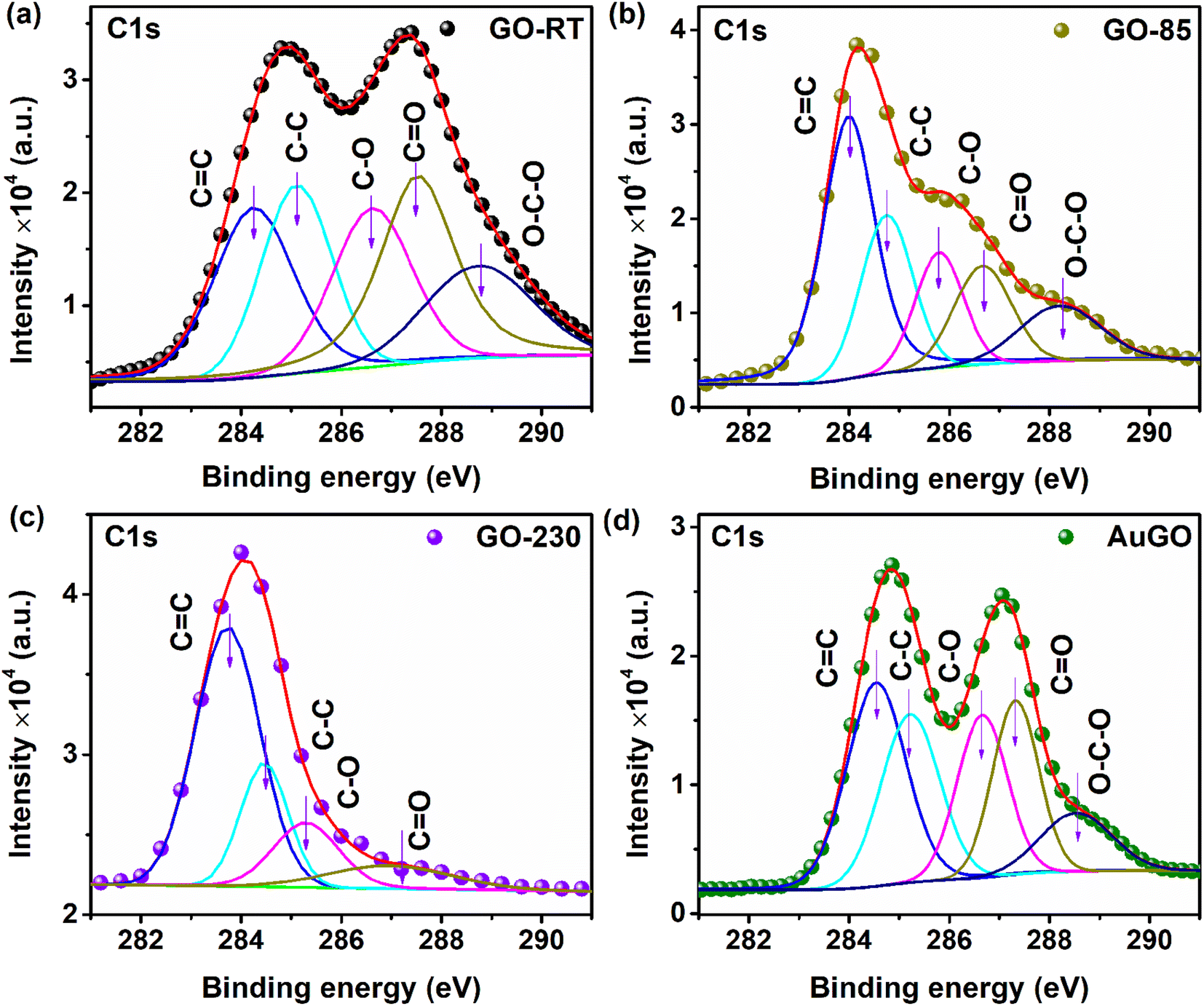 | ||
| Fig. 2 C 1s XPS spectra with the fitting for (a) GO-RT, (b) GO-85, (c) GO-230, and (d) AuGO. | ||
Fig. S3a and b† illustrate the XPS survey spectra and Au 4f spectra of AuGO, respectively. The survey spectrum reveals two prominent peaks corresponding to O 1s (∼533 eV) and C 1s (∼285 eV), distinct from substrate peaks, with a lower intensity peak for Au 4f (84 eV), highlighted by a red circle in Fig. S3a.† Deconvolution of the Au 4f peaks for AuGO reveals two distinct peaks, Au 4f7/2 at 83.5 eV and Au 4f5/2 at 87.3 eV, as depicted in Fig. S3b,† confirming the presence of Au NPs.
The analysis of the degree of oxygen functional groups attached to the GO can be conducted using FTIR spectra, as illustrated in Fig. S3(c and d).† The transmittance peaks in the spectra of GO samples are investigated within the range of 900 cm−1 to 3600 cm−1. Notably, a broadened peak at 3400 cm−1 is associated with –OH, likely stemming from the absorption of water molecules on GO from the environment; this peak diminishes in GO-230. Additionally, peaks at 1623 cm−1 and 1715 cm−1 correspond to C–C and CC, respectively. Peaks within the FTIR spectra ranging from 950 cm−1 to 1480 cm−1 signify the presence of oxygen functional groups. Specially, peaks at 1040 cm−1, 1163 cm−1, and 1396 cm−1 are attributed to C–O, CO, and O–CO, respectively.27,28 Notably, the oxygen functional groups appear more pronounced in GO-RT than GO-85, GO-120, and GO-230. In GO-230, the peak at 1396 cm−1 related to the O–CO disappears, while the intensity of the peak at 1040 cm−1 and 1163 cm−1, associated with C–O and CO, respectively, decreases. The 1040 cm−1 peak stands out prominently among other oxygen functional groups, while the 1715 cm−1 peak is associated with sp2 carbon. The relative change in the oxygen functional groups in GO with the annealing is determined using the intensity ratio of 1040 cm−1 (C–O) and 1715 cm−1 (CC) peaks (IC–O/ICC), as depicted in Fig. S3d.† The results suggest a gradual reduction in C–O groups within the GO structure as the annealing temperature increases. However, the graphitic peaks at 1623 cm−1 and 1715 cm−1 are present across all the GO samples.
Electron diffraction spectroscopy (EDS) is employed to analyze the elemental composition of GO-RT before and after annealing (Fig. S4†). The atomic weight percentage (at%) of carbon in GO-RT (Fig. S4a†), GO-85 (Fig. S4d†), and GO-230 (Fig. S4e†) is measured to be 50.54%, 70.3%, and 85.3%, respectively, while the percentages of oxygen are 49.46%, 29.3%, and 14.7%, respectively. Additionally, EDS area mapping is conducted on GO-RT and AuGO. The area of GO-RT is shown in the inset of Fig. S4a.† The uniform distribution of carbon and oxygen in the pictorial image of GO-RT is evident in Fig. S4b and c,† respectively. Elemental compositions, such as Au, C, and O of AuGO, are depicted in Fig. S4f,† and the mapping area of AuGO is illustrated in the inset of Fig. S4f.† The at% of Au, C, and O in the AuGO are determined as 0.42%, 48.4%, and 51.18%, respectively. The sparse distribution of Au on the AuGO is observed in the pictorial image shown in Fig. S4g,† correlating with the FESEM image of Au NPs decorated on GO (inset of Fig. S4f†). The high concentration of C and O in the AuGO is discernible in the pictorial images in Fig. S4h and i,† respectively. Hence, GO-RT exhibits a significant presence of oxygen functional groups, while GO-230 exhibits substantially reduced functional groups. The analyses of the XRD, Raman, XPS, FTIR, and EDS corroborate this observation.
4.2. Electrical characterizations
The optoelectronic properties of GO are analyzed based on the degree of oxygen functional groups attached to the GO and Au NPs decorated on the GO (AuGO) devices. The FESEM image of the GO sheets and the GO sheets on the IDE pattern are shown in Fig. 3a and the inset of Fig. 3a, respectively. The GO sheets entirely cover the metal fingers, displaying prominent wrinkles, resulting from oxidation during the chemical synthesis process. The presence of Au NPs decorated on the GO sheet and the AuGO device is depicted in Fig. 3b and its inset. The Au NPs exhibit a homogeneous distribution on the GO sheet, as observed in Fig. 3b, with an average diameter of approximately 100 nm. Bright lines on the GO sheet represent the wrinkles commonly observed in large lateral-size GO. Sparsely deposited Au NPs are observed on the metal fringes of the IDE pattern and within the channel region of the Au NPs deposited on the GO device (AuGO), as illustrated in the inset of Fig. 3b.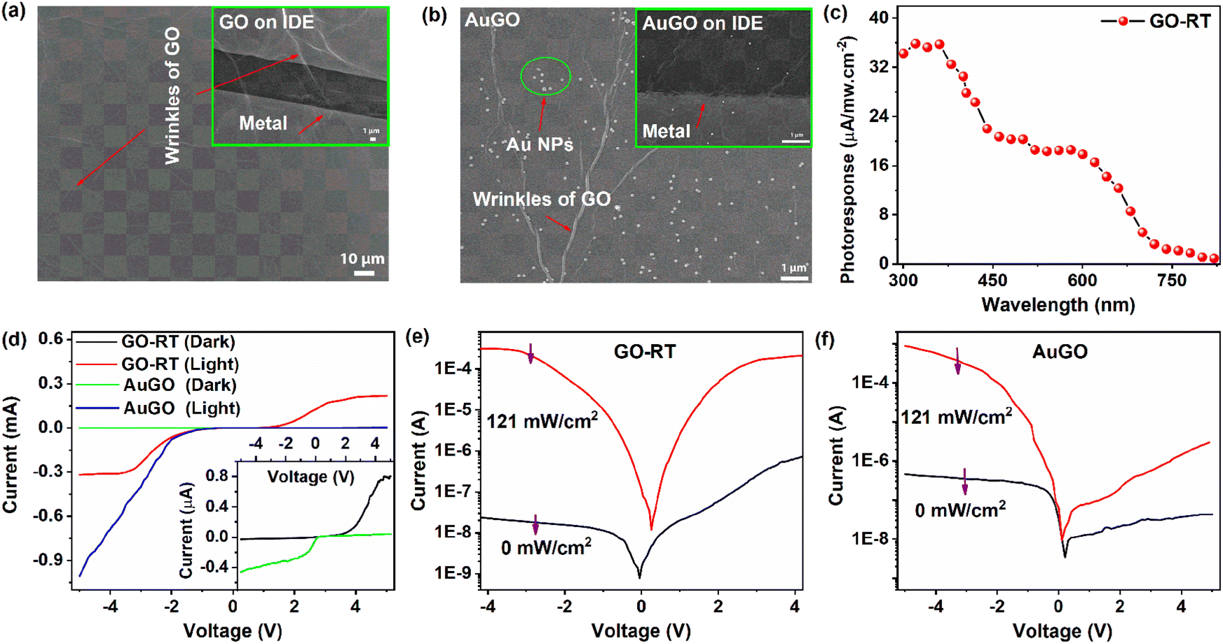 | ||
| Fig. 3 (a) FESEM image of the GO sheet (inset: GO sheet on the IDE pattern); (b) FESEM image of Au NPs decorated on the GO sheet (inset: AuGO on the IDE pattern); (c) spectral photoresponse of GO-RT as a function of incident wavelengths; (d) I–V curves for AuGO and GO-RT in dark and under light (405 nm) illumination, with magnified curves at low applied voltage (inset); (e and f) logI–V curves of the dark and light illumination for GO-RT and AuGO, respectively. | ||
The photo-response characteristics of GO with varying levels of oxygen functional groups on a p-type Si substrate (p-Si) and Au NPs deposited on GO-RT are investigated. Photocurrent (Iph) is determined by the difference between the photo-induced current (Ilight) and dark current (Idark). In Fig. 3c, the photoresponse of GO-RT within the wavelength range of 300 nm to 820 nm is measured by calculating the ratio of Iph to the intensity of the exposing wavelength. The spectral photoresponse is measured using a broad-spectrum light source (xenon lamp), monochromator, and reflective mirror. The intensity of the light falling on the sample is lower than that of the laser (405 nm) due to several stages of light filtration, resulting in decreased intensity. The light intensity varies for each wavelength and is notably lower in the UV region. The photo-responsive behavior of GO-RT across different wavelengths is illustrated in Fig. 3c, showing a higher response in the UV region that gradually diminishes towards the visible-IR range. A 405 nm laser is selected to analyze the photo-response speed of the GO-based devices in this experiment.
The I–V characteristics of GO-RT and AuGO are measured in both dark and light environments, as shown in Fig. 3d. These characteristics appear asymmetric, supported by the observation that the Ilight under negative bias is higher than that under positive bias. The Idark gradually increases with increased bias voltage, whereas the Ilight intensifies rapidly after raising the bias voltage, as depicted in Fig. 3d and f.
The photoresponse of AuGO and GO-based devices is more active under negative bias voltage; hence, further characterizations are performed under this condition. The Idark of GO-RT and AuGO are measured as −20 nA and −372 nA, respectively. The high Idark of AuGO may be attributed to the enhanced electrical conductivity property of Au NPs and the induced electron tunneling effect.29 The Ilight values for GO-RT and AuGO are recorded at 0.3 mA and 0.52 mA, respectively. The I–V characteristics in both dark and light illumination for GO-RT and AuGO are presented in Fig. 3e and f, and those of GO-85, GO-120, and GO-230 are demonstrated in Fig. S5a–c,† respectively. The Ilight for GO-RT, GO-85, GO-120, and GO-230 are −300 μA, −113 μA, −69.54 μA, and −68.65 μA, respectively. Correspondingly, the Idark values are −20 nA, −40 nA, −128 nA, and −496 nA, respectively. Thus, the photocurrent on/off ratio is the highest (1.5 × 10⁴) for GO-RT and is the lowest (1.38 × 10²) for GO-230. Thus, the increase in the annealing temperature of GO leads to a reduction in Ilight accompanied by the rise in Idark. This reduction in Ilight may be attributed to removing oxygen functional groups from the GO. In contrast, the rise in Idark is due to the restoration of sp2 hybridized carbon atoms after thermal treatments, corroborated by the XRD, Raman, and XPS spectra analysis. A shifting of the bias voltage for the lowest Ilight is observed for all the samples, indicating a self-bias property. Among the devices, GO-230 exhibits a prominent Ilight of 1.44 μA at 0 V in the I–V curve, the highest among them. Further analysis uses a bias voltage of −3.5 V and light intensity of 121 mW cm−2 (at 405 nm).
4.3. Origin of high photocurrent in GO
The generation of Iph in the GO-based devices is attributed to the photoconductive effect, where incident light at responsive wavelengths produces free charge carriers in the GO, augmenting the Iph. The working mechanism of the GO-based devices is elucidated through a schematic diagram presented in Fig. 4, explaining its operations in both dark and light illumination. The conduction band (Ec) and valence band (Ev) energy levels for highly functionalized GO are measured as −3.4 eV and −6.3 eV, respectively, referenced to the vacuum level.17 Si exhibits energy levels of −4.3 eV for Ec and −5.4 eV for Ev. In the dark, fewer charge carriers transfer from the GO's Ec to the Si's Ec due to the disruption caused by attached oxygen functional groups. Notably, GO-RT demonstrates a lower dark current than other samples with less oxygen-functional groups.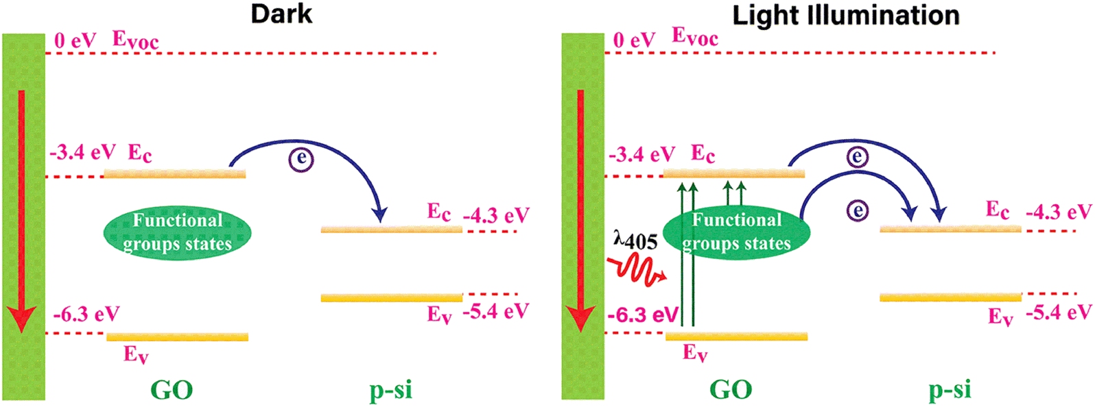 | ||
| Fig. 4 The charge transfer mechanism in GO-RT under dark and under light illumination. | ||
The light illumination by a 405 nm laser on the GO device generates extra charge carriers in three potential ways: (a) the 405 nm irradiated laser generates electron–hole pairs in the GO due to its band gap of 2.9 eV. The resulting electrons move to the Si's Ec, contributing to the current flow. (b) Photo-generated charge carriers move from the defect states created by oxygen functional groups to the GO's Ec. Subsequently, these charge carriers move to the Si's Ec, aiding current flow. (c) Charge carriers flow directly from the defect states of GO to the Si's Ec due to the broad distribution of defect states between the Ec and Ec of highly oxidized GO. These defect states notably contribute to the increased photocurrent in GO-RT, wherein the degree of defect states relies on the presence of oxygen functional groups. A reduction or partial removal of oxygen functional groups would diminish the photocurrent. Consequently, GO-RT exhibits a much higher photocurrent than GO-230, GO-120, and GO-85.
The electrical characteristic of the GO-RT is changed after the decoration of Au NPs on the GO sheets, such as an increase of dark current (explained in section 4.2) and localized surface plasmon resonance (LSPR) of Au NPs.30 The LSPR phenomenon improves the absorption of GO by trapping light at the GO–Au NP interface. This influence is intensified by the combination of several Au NPs, leading to the localization of scattered light around them and a significant enhancement in light absorption. Overall, the LSPR effect thereby improves both conductivity and photoelectric responsivity. The interaction between Au NPs and GO is evident in the shifting of absorbance peak positions for GO and Au NPs. Our inference is also supported by the discussion involving the enhancement in the PL intensity after decoration of Au NPs on the sheet in the preceding section 4.1. The Raman and XPS spectral analysis also validate our hypothesis of interaction between Au NP and GO due to charge transfer. Thus, the overall increase in the photocurrent is due to the combined effect of charge transfer as well as LSPR.
4.4. Performance of GO-based photodetector
This section analyzes GO-based photodetectors' performance based on photo-response, responsivity, external quantum efficiency, and response time. The light current represents the current during light irradiation, while Iph is the difference between light current and dark current under identical conditions. A constant negative bias voltage of −3.5 V is applied, along with varying intensity of pulse laser excitation at 405 nm, for AuGO (Fig. 5a), GO-RT (Fig. S6a†), GO-85 (Fig. S6b†), GO-120 (Fig. S6c†), and GO-230 (Fig. S6d†). The photoresponse of AuGO gradually increases as the laser intensity ranges from 0.05 mW cm−2 to 1.43 mW cm−2, as depicted in the inset of Fig. 5a. It rises rapidly up to 205 mW cm−2. The power-dependent photoresponse of AuGO is analyzed using the power law equation Iph = APθ, where Iph represents photocurrent, A is the proportionality constant, P signifies the intensity/incident power density of the laser, and θ denotes the slope/response of Iph to light intensity.7 The slope (θ) is derived from the exponential graph of Iphvs. light intensity (Fig. 5b). AuGO exhibits a θ value of 1.11, showcasing a highly linear relationship between photo-generated free charge carriers and incident light flux. Ideally, θ should be 1, but the fitted θ value is comparable, indicating minimal recombination of photo-generated charge carriers and some contribution of trap losses to Iph. The non-ideal value (θ = 1.11) may result from a fraction of trapped and recombined free charge carriers.31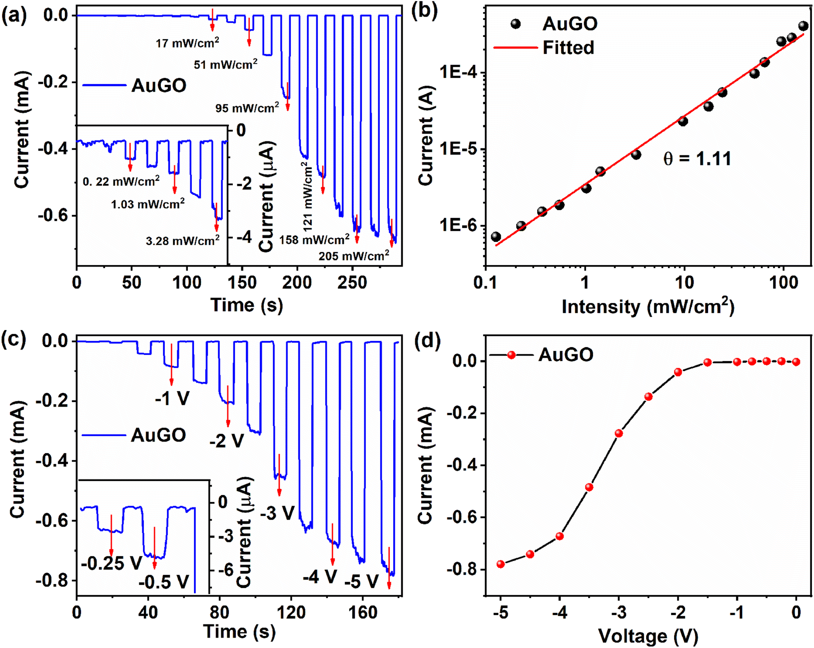 | ||
| Fig. 5 (a) Temporal photocurrent response of AuGO at different intensities of the laser (405 nm); the inset shows the photocurrent response at low intensities; (b) a logarithmic plot of the photocurrent vs. laser intensities at −3.5 V; (c) temporal photocurrent response of AuGO at different bias voltages; the inset displays the photocurrent response at low bias voltages; and (d) the variation of photocurrent as a function of bias voltage for AuGO with laser power: 121 mW cm−2. | ||
For GO-RT, GO-85, GO-120, and GO-230, the θ values are 1.12, 1.07, 1.01, and 0.96, respectively (inset of Fig. S6a and b†), indicating a substantial contribution of photo-generated free charge carriers to Iph in these GO-based devices. Values of θ < 1 may be attributed to the presence of defect states or surface states. The gradual reduction in θ from 1.12 to 0.96 for GO-RT, GO-85, GO-120, and GO-230 reflects increasing structural defects post-thermal annealing and removal of oxygen functional groups. Conversely, θ > 1 for other devices may stem from a higher presence of oxygen functional groups trapping a fraction of charge carriers,32 which is challenging to justify from a single effect.
The evolution from the semiconducting character of GO to a nearly metallic nature (RGO) is depicted in Fig. S7.† The correlation of Iph with bias voltage is explored for GO-RT (Fig. S7a†), GO-85 (Fig. S7b†), GO-120 (Fig. S7c†), and GO-230 (Fig. S7d†). The temporal light current is assessed under constant light intensity (121 mW cm−2). In Fig. 5c, the llight of AuGO notably increases at reverse bias voltages ranging from −1.5 V to −4.0 V. However, the current gradually increases between 0 V and <−1.0 V (inset of Fig. 5c) and from −4.0 V to −5.0 V. The lower light current below −1.0 V may result from insufficient energy to facilitate the flow of free photo-generated charge carriers from the active materials to the metal electrode. This leads to charge carrier recombination before separation and, subsequently, a low current.33 The gradual increase in light current post −4.0 V for AuGO might indicate nearing saturation. The rapid increase in Iph between −1.0 V and −4.0 V could be due to the swift transport of photo-generated charge carriers to the metal electrode, preventing charge carrier recombination.32 The Iph related to reverse bias voltage is analyzed through plotted graphs of Iph against bias voltage (Fig. S7a–d†) for GO-RT, GO-85, GO-120, and GO-230. In GO-RT, a transition in Ilight is observed from −1 V to −3.5 V, and the saturated Iph is −0.29 mA at an applied bias voltage of −3.5 V (Fig. S7a†). Although the light current gradually increases from −3.5 V to −5.0 V, the Iph remains constant, possibly due to the rise in dark current compromising the increase in light current. Asymmetric Iph behavior is observed in GO-85 and GO-120. GO-230 demonstrates an almost linear curve among different devices, indicative of its ohmic characteristics. The restoration of the sp2 hybridized structure in GO by removal of oxygen functional groups leads to the conversion of semiconducting behavior to a metallic behavior. Fig. 5d shows the variation of photocurrent as a function of bias voltage for AuGO with a laser power of 121 mW cm−2. The non-linear relationship between the photocurrent (Iph) and applied bias voltage (V) could be explained as follows. As the GO behaves like a semiconductor, the photocurrent is essentially proportional to the depletion width in the junction and diffusion lengths of carriers. The depletion width is nonlinearly dependent on the applied reverse bias, and as a result, the photocurrent varies nonlinearly with the applied bias, as shown.
The temporal light current analysis of GO-based devices is presented in Fig. 6a, distinguishing the contribution of Ilight from the localized surface plasmon resonance (LSPR) of Au NPs, enhanced charge transfer from GO to the external contacts,30 and different oxygen functional groups in GO, such as highly oxygenated GO (GO-RT) and low-oxygenated GO (GO-230). The Ilight of GO-RT is notably higher than GO-85, GO-120, and GO-230. This disparity arises due to the presence of abundant oxygen functional groups that contribute more charge carriers during light irradiation, as explained previously. Specifically, the Ilight values for AuGO, GO-RT, GO-85, GO-120, and GO-230 are −0.485 mA, −0.225 mA, −0.171 mA, −0.151 mA, and −0.148 mA, respectively. Correspondingly, the Idark values for AuGO, GO-RT, GO-85, GO-120, and GO-230 are −34 nA, −253 nA, −602 nA, −678 nA, and −363 nA, respectively.
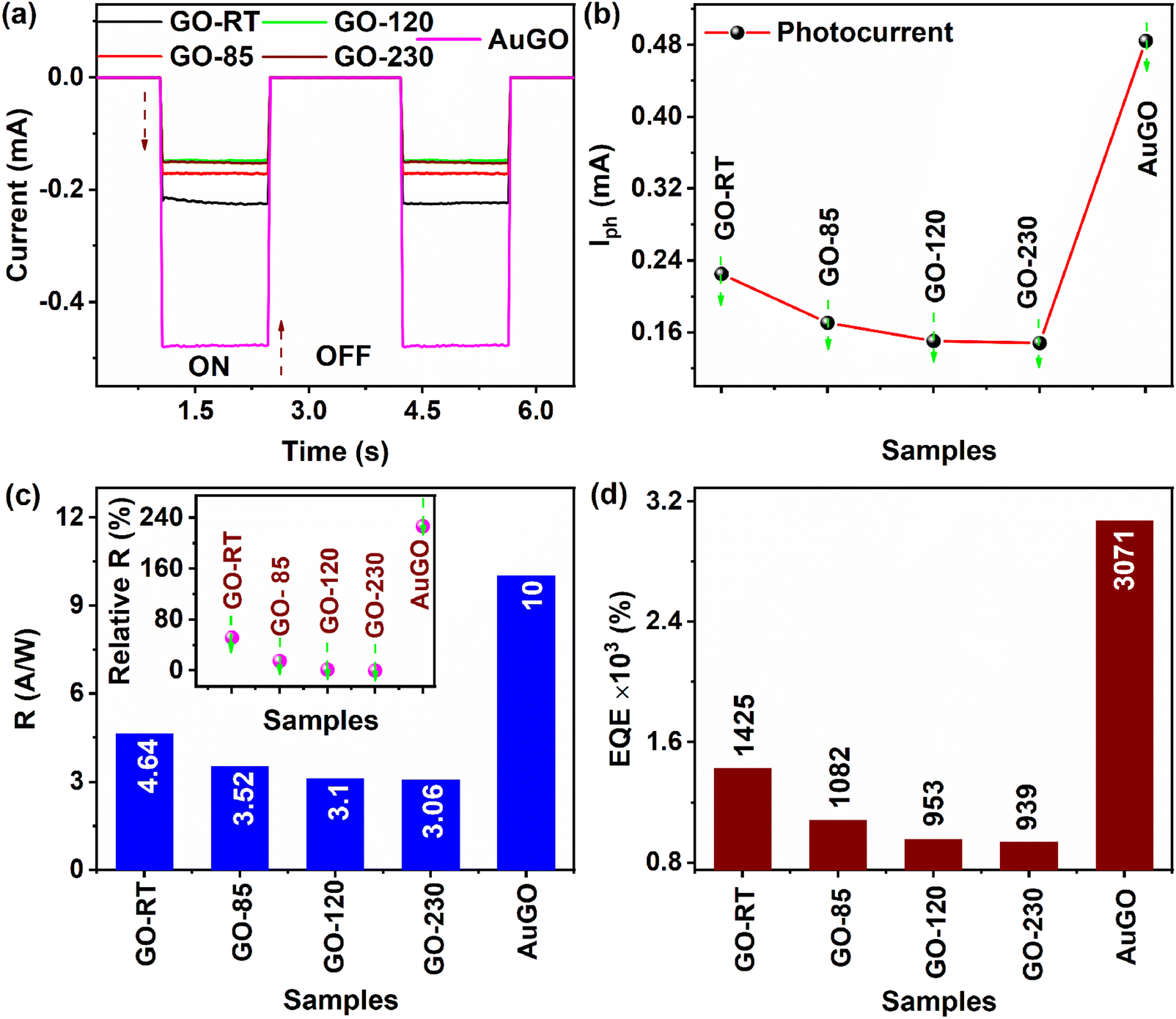 | ||
| Fig. 6 (a) Photocurrent response of annealed GO and AuGO exposed to a pulsed laser (405 nm) under identical conditions; (b) photocurrent (Iph) magnitude for different samples; (c) measured responsivity (R) for different samples; the inset shows the percentage enhancement of R relative to GO-230; and (d) comparison of the external quantum efficiency (EQE) of GO-RT, GO-85, GO-120, GO-230, and AuGO. | ||
AuGO demonstrates an increased Ilight, reaching up to 255 μA and 332 μA compared to GO-RT and GO-230, respectively. This increase is attributed to heightened light absorption in AuGO, thereby augmenting higher Ilight in AuGO.30 GO-RT exhibits an Ilight 1.5 times greater than GO-230, potentially due to the abundant oxygen functional groups present in GO-RT. The Ilight observed in GO-230 (−0.148 μA) may originate from structural defects, as there is a reduction in oxygen functional groups from GO-230, as revealed from XPS and FTIR analyses. Ultimately, the combined effects of the plasmonic effect and abundant oxygen functional groups contribute to a 3.24 times enhancement in AuGO's Ilight compared to GO-230.
4.5. Figures of merit of the GO-based photodetector
The performance of the photodetector is determined by several parameters30,31,34,35 including photocurrent (Iph), on/off ratio (RON/OFF), responsivity (R), external quantum efficiency (EQE), detectivity (D), noise equivalent power (NEP) and response time (rise and fall).I ph represents the difference in current between the light current and dark current of a photodetector device. It is calculated using a formula:
| Iph = Ilight − Idark | (1) |
R ON/OFF is the ratio of a photodetector's light current to its dark current.3 A device with a high RON/OFF can detect low incident light, and this can be enhanced by reducing the Idark, promoting fast photo generation of free charge carriers, and increasing the Ilight. The RON/OFF is calculated using the following formula:
 | (2) |
The responsivity, R, can be defined as the generation of Iph in the active material of a photodetector per unit intensity of the incident light; it is measured in A W−1. The R values of the GO-based devices are calculated using the following formula:36
 | (3) |
EQE, known as the amount of free charge carriers generated in the device per unit of incident photons, is calculated using the following formula:3
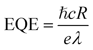 | (4) |
Detectivity (D) can be calculated using the following equation:31
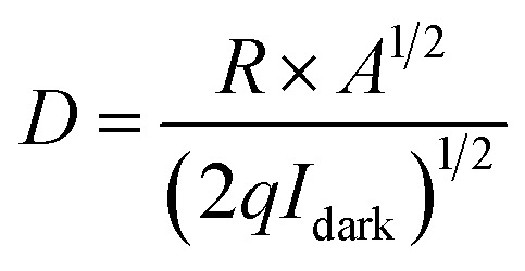 | (5) |
Noise equivalent power (NEP) is calculated using the following formula:37
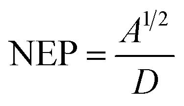 | (6) |
Response time is the duration a photodetector takes to respond to the incident light. It is analyzed in terms of rise time (τrise) and fall time (τfall). τrise is the time required to reach the saturated light current from the dark current of a photodetector. τfall is determined as the time required to decline from the saturated light current to the dark current level of a photodetector. It can be calculated using the following equation:31
| Iph(t) = I0 + Ae−t/τ | (7) |
The response time of the GO-based devices is analyzed using temporal response measurements. The fast temporal response is measured by applying a 20 kHz pulse generator on the laser (405 nm) and a bias voltage of −5 V, then capturing the response data using a digital oscilloscope. The response data perfectly fits the τrise and τfall of the GO-based devices using eqn (7), shown in Fig. 7. The τrise GO-RT, AuGO, and GO-230 is measured as 8.21 μs, 24.19 μs, and 27.8 μs, respectively; the τrise of GO-RT is 2.94 times faster than AuGO, and 3.38 times faster than GO-230. The τfall of GO-RT, GO-230, and AuGO is 295.15 μs, 208.9 μs, and 147.6 μs, respectively. The τfall of AuGO is 86.25 μs less than GO-RT and 61.3 μs more than GO-230. These results illustrate that GO-based devices can effectively detect high-frequency light signals. The fast response time of GO-RT may be attributed to direct charge transfers from the intermediate energy states without trapping the generated charge carriers during light irradiation.
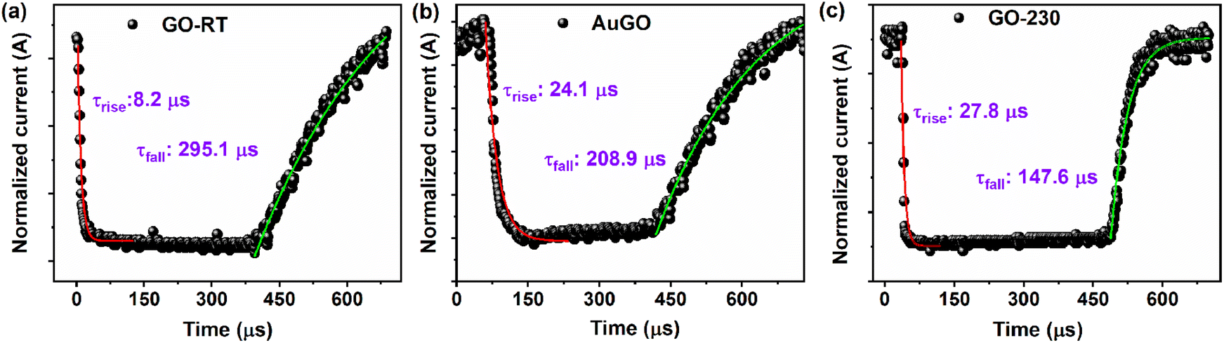 | ||
| Fig. 7 The rise time and fall time of (a) GO-RT, (b) AuGO, and (c) GO-230 photodetectors with exponential fits. | ||
Conversely, the slower response time of GO-230 compared to GO-RT and AuGO could be due to the creation of the defect states in the annealed GO after the removal of oxygen functional groups, which act as trapping sites for charge carriers. The presence of abundant oxygen functional groups in GO-RT is explained in the previous section, and the removal of these oxygen functional groups by thermal annealing of GO creates structural defects, as confirmed by the broad peak at 25.6° observed in the XRD of GO-230. Therefore, the synergy between abundant oxygen functional groups and the induced charge carriers by the decorated Au NPs significantly contributes to enhancing the photo-sensing response of GO.
5. Conclusions
We investigated the effects of oxygen functional groups and plasmonic Au NPs on photo absorption, followed by photodetection on large-area GO sheets. The existence of oxygen functional groups in GO, along with their systematic reduction through thermal annealing at various temperatures, has been confirmed by XPS, Raman, EDS, and FTIR spectroscopy. The notable shift in the characteristic XRD peak for the 〈002〉 plane, from 10.9° to 25.6°, further verifies the reduction of functional groups and the restoration toward graphitic structures. Moreover, the broader peak at 25.6° indicates the creation of structural defects during the thermal annealing of GO. The sparse decoration of Au NPs on the GO surface, confirmed in the FESEM image, is also evident in the UV-Vis absorption spectrum, which enhances absorption in the UV-visible region. The influence of functional groups is apparent in the performance of GO-based photodetectors, where Iph decreases from 0.225 mA to 0.148 mA due to functional group reduction. However, Iph significantly increases to 0.484 mA after incorporating Au NPs onto the GO surfaces. The Au NP-decorated GO exhibits the highest responsivity of 10 A W−1, 3.3 times higher than fully reduced GO and 2.1 times higher than GO. The EQE of AuNP-decorated GO increases to 3071% from 939% of reduced GO and 1425% of GO. Additionally, AuGO and GO-RT demonstrate superior photo-sensing capabilities compared to other reported values. In conclusion, the presence of oxygen functional groups on GO enhances the performance of GO-based photodetectors, as confirmed by the material characterization of GO. These results are significant for developing GO-based photodetectors and other optoelectronic devices. The performance of GO-based photodetector devices can be further studied by changing the thickness of GO from thin film to single/bi-layer, 2-electrode to three terminals (transistor-based photodetector device), different work function metals used as electrodes, and asymmetric channel width of IDE patterns, etc. The stability of the GO-based device may be a concern for practical application, which can be improved by proper encapsulation.Author contribution
Ningthoujam Somorjit Singh (conceptualization, investigation, methodology, writing-original draft); Abdul Kaium Mia (assist experiment and analysis data); P. K. Giri (conceptualization, funding acquisition, supervision, writing – review & editing).Conflicts of interest
The authors declare no conflict of interest.Acknowledgements
The authors acknowledge the MEITY (Grant No. 5(9)/2022-NANO (VOL-II)) and SERB (Grant No. CRG/2021/006397) for partly funding this research. The authors also acknowledge the technical support from the Central Instrumentation Facility, I.I.T. Guwahati, and thank Sirsendu Ghosal for providing Au NPs.References
- A. K. Geim and K. S. Novoselov, Nat. Mater., 2007, 6, 183–191 CrossRef CAS PubMed.
- K. Krishnamoorthy, M. Veerapandian, K. Yun and S. J. Kim, Carbon, 2013, 53, 38–49 CrossRef CAS.
- M. A. Khan, A. Kumar, J. Zhang and M. Kumar, J. Mater. Chem. C, 2021, 9, 8129–8157 RSC.
- B. Ezhilmaran, A. Patra, S. Benny, M. R. Sreelakshmi, V. V. Akshay, S. V. Bhat and C. S. Rout, J. Mater. Chem. C, 2021, 9, 6122–6150 RSC.
- P. S. Abid, S. S. Islam, P. Mishra and S. Ahmad, Sci. Rep., 2018, 8, 1–13 CAS.
- J. Jiang, Y. Wen, H. Wang, L. Yin, R. Cheng, C. Liu, L. Feng and J. He, Adv. Electron. Mater., 2021, 7, 202001125 Search PubMed.
- L. Zheng, L. Zhongzhu, S. Guozhen, K. Zhang, L. Zhang, L. Han, L. Wang, Z. Chen, H. Xing, X. Chen, H. Qiao, Z. Huang, X. Ren, S. Liu, Y. Zhang, X. Qi, H. Zhang, M. Long, P. Wang, H. Fang, W. Hu, J. Jiang, Y. Wen, H. Wang, L. Yin, R. Cheng, C. Liu, L. Feng, J. He, N. Huo, G. Konstantatos, B. Ezhilmaran, A. Patra, S. Benny, M. R. Sreelakshmi, V. V. Akshay, S. V. Bhat and C. S. Rout, Adv. Funct. Mater., 2021, 7, 1–27 Search PubMed.
- G. Li, L. Liu, G. Wu, W. Chen, S. Qin, Y. Wang and T. Zhang, Small, 2016, 12, 5019–5026 CrossRef CAS PubMed.
- Y. Cao, J. Zhu, J. Xu, J. He, J. L. Sun, Y. Wang and Z. Zhao, Small, 2014, 10, 2345–2351 CrossRef CAS PubMed.
- S. K. Lai, L. Tang, Y. Y. Hui, C. M. Luk and S. P. Lau, J. Mater. Chem. C, 2014, 2, 6971–6977 RSC.
- X. An, F. Liu, Y. J. Jung and S. Kar, Nano Lett., 2013, 13, 909–916 CrossRef CAS PubMed.
- B. Chitara, S. B. Krupanidhi and C. N. R. Rao, Appl. Phys. Lett., 2011, 99, 1–4 CrossRef.
- N. S. Singh, F. Mayanglambam, H. B. Nemade and P. K. Giri, RSC Adv., 2021, 11, 9488–9504 RSC.
- V. G. Sreeja, G. Vinitha, R. Reshmi, E. I. Anila and M. K. Jayaraj, Opt. Mater., 2017, 66, 460–468 CrossRef CAS.
- L. Wu, W. Li, P. Li, S. Liao, S. Qiu, M. Chen, Y. Guo, Q. Li, C. Zhu and L. Liu, Small, 2014, 10, 1421–1429 CrossRef CAS PubMed.
- Y. Zhou, X. Lin, Y. Huang, Y. Guo, C. Gao, G. Xie and Y. Jiang, Sens. Actuators, B, 2016, 235, 241–250 CrossRef CAS.
- N. S. Singh, F. Mayanglambam, H. B. Nemade and P. K. Giri, ACS Appl. Nano Mater., 2022, 5, 6352–6364 CrossRef CAS.
- S. Claramunt, A. Varea, D. López-Díaz, M. M. Velázquez, A. Cornet and A. Cirera, J. Phys. Chem. C, 2015, 119, 10123–10129 CrossRef CAS.
- I. Ogino, Y. Yokoyama, S. Iwamura and S. R. Mukai, Chem. Mater., 2014, 26, 3334–3339 CrossRef CAS.
- L. G. Cançado, A. Jorio, E. H. M. Ferreira, F. Stavale, C. A. Achete, R. B. Capaz, M. V. O. Moutinho, A. Lombardo, T. S. Kulmala and A. C. Ferrari, Nano Lett., 2011, 11, 3190–3196 CrossRef PubMed.
- D. Long, W. Li, L. Ling, J. Miyawaki, I. Mochida and S. H. Yoon, Langmuir, 2010, 26, 16096–16102 CrossRef CAS PubMed.
- C. H. Chuang, Y. F. Wang, Y. C. Shao, Y. C. Yeh, D. Y. Wang, C. W. Chen, J. W. Chiou, S. C. Ray, W. F. Pong, L. Zhang, J. F. Zhu and J. H. Guo, Sci. Rep., 2014, 4, 1–7 Search PubMed.
- H. Zhao, S. Fan, Y. Chen, Z. Feng, H. Zhang, W. Pang, D. Zhang and M. Zhang, ACS Appl. Mater. Interfaces, 2017, 9, 40774–40781 CrossRef CAS PubMed.
- M. Koinuma, H. Tateishi, K. Hatakeyama, S. Miyamoto, C. Ogata, A. Funatsu, T. Taniguchi and Y. Matsumoto, Chem. Lett., 2013, 42, 924–926 CrossRef CAS.
- S. Lin, Z. Fang, J. Ma, D. Guo, X. Yu, H. Xie and M. Fang, Small Methods, 2024, 8, 2300716 CrossRef CAS PubMed.
- L. P. L. Mawlong, K. K. Paul and P. K. Giri, Nanotechnology, 2021, 32, 215201 CrossRef CAS PubMed.
- M. Aliahmad and M. Dehbashi, Iran. J. Energy Environ., 2013, 4, 53–59 Search PubMed.
- E. M. Deemer, P. K. Paul, F. S. Manciu, C. E. Botez, D. R. Hodges, Z. Landis, T. Akter, E. Castro and R. R. Chianelli, Mater. Sci. Eng. B, 2017, 224, 150–157 CrossRef CAS.
- K. Y. Chan, D. Yang, B. Demir, A. P. Mouritz, H. Lin, B. Jia and K. T. Lau, Composites, Part B, 2019, 178, 107480 CrossRef CAS.
- Q. Wang, Y. Tu, T. Ichii, T. Utsunomiya, H. Sugimura, L. Hao, R. Wang and X. He, Nanoscale, 2017, 9, 14703–14709 RSC.
- S. Parveen, M. Das, S. Ghosh and P. K. Giri, Nanoscale, 2022, 6402–6416 RSC.
- R. Kumar, M. A. Khan, A. V Anupama, S. B. Krupanidhi and B. Sahoo, Appl. Surf. Sci., 2021, 538, 148187 CrossRef CAS.
- S. Debnath, K. Ghosh, M. Meyyappan and P. K. Giri, Nanoscale, 2023, 15, 13809–13821 RSC.
- P. S. Abid, C. M. Julien and S. S. Islam, ACS Appl. Mater. Interfaces, 2020, 12, 39730–39744 CrossRef CAS PubMed.
- A. Bora, L. P. L. Mawlong and P. K. Giri, ACS Appl. Electron. Mater., 2021, 3, 4891–4904 CrossRef CAS.
- M. T. Hossain, M. Das, J. Ghosh, S. Ghosh and P. K. Giri, Nanoscale, 2021, 13, 14945–14959 RSC.
- Y. Wang, S. Yang, D. R. Lambada and S. Shafique, Sens. Actuators, A, 2020, 314, 112232 CrossRef CAS.
- C. Bonavolontà, A. Vettoliere, G. Falco, C. Aramo, I. Rendina, B. Ruggiero, P. Silvestrini and M. Valentino, Sci. Rep., 2021, 11, 1–10 CrossRef PubMed.
- X. Qi, X. Zou, Z. Huang, L. Ren, G. Hao, Y. Liu, X. Wei and J. Zhong, Appl. Surf. Sci., 2013, 266, 332–336 CrossRef CAS.
- Y. Luo, X. Yan, J. Zhang, B. Li, Y. Wu, Q. Lu, C. Jin, X. Zhang and X. Ren, Nanoscale, 2018, 10, 9212–9217 RSC.
- D. Alsaedi, M. Irannejad, K. Ibrahim, A. Almutairi, K. Musselman, J. Sanderson, O. Ramahi and M. Yavuz, ACS Appl. Electron. Mater., 2020, 2, 1203–1209 CrossRef CAS.
- J. An, T. S. D. Le, C. H. J. Lim, V. T. Tran, Z. Zhan, Y. Gao, L. Zheng, G. Sun and Y. J. Kim, Adv. Sci., 2018, 5, 1–9 Search PubMed.
- P. Nath, S. Chowdhury, D. Sanyal and D. Jana, Carbon, 2014, 73, 275–282 CrossRef CAS.
Footnote |
| † Electronic supplementary information (ESI) available: XPS analysis, EDS analysis, logarithmic I–V curves for GO-85, GO-120, and GO-230, AuGO; power-dependent measurement of the photo-response current for the GO-RT, GO-85, GO-120, and GO-230; voltage-dependent measurement of the photo-response current for the GO-RT, GO-85, GO-120, and GO-230; on/off ratio, and detectivity curve. See DOI: https://doi.org/10.1039/d3na01120h |
| This journal is © The Royal Society of Chemistry 2024 |