
 Open Access Article
 This Open Access Article is licensed under a Creative Commons Attribution-Non Commercial 3.0 Unported Licence
Tunable, multifunctional opto-electrical response in multilayer FePS3/single-layer MoS2 van der Waals p–n heterojunctions†
Maria
Ramos‡
 ab,
Marcos
Gadea‡
ab,
Samuel
Mañas-Valero
c,
Carla
Boix-Constant
c,
Eudomar
Henríquez-Guerra
ab,
María A.
Díaz-García
ab,
Eugenio
Coronado
c and
M. Reyes
Calvo
*ab
ab,
Marcos
Gadea‡
ab,
Samuel
Mañas-Valero
c,
Carla
Boix-Constant
c,
Eudomar
Henríquez-Guerra
ab,
María A.
Díaz-García
ab,
Eugenio
Coronado
c and
M. Reyes
Calvo
*ab
aDepartamento de Física Aplicada, Universidad de Alicante, Alicante 03080, Spain. E-mail: reyes.calvo@ua.es
bInstituto Universitario de Materiales de Alicante (IUMA), Universidad de Alicante, Alicante 03080, Spain
cInstituto de Ciencia Molecular (ICMol), Universitat de València, Paterna 46980, Spain
First published on 26th February 2024
Abstract
The combination of specific van der Waals semiconductors in vertical stacks leads to atomically sharp heterointerfaces with unique properties, offering versatility and additional functionality for thin, flexible, optoelectronic devices. In this work, we demonstrate heterostructures built from single-layer MoS2 (n-type) and multilayer FePS3 (p-type) as multifunctional p–n junctions where robust photoluminescent light emission and broadband electrical photo-response coexist. This is made possible by the inherent properties of the materials involved and the precise energy band alignment at their interface, which preserves the photoluminescent emission provided by the single-layer MoS2 and confers exceptional tunability to the system. Indeed, through small changes in the applied voltage across the junction, the interplay between photoluminescence and photocurrent generation can be tuned, allowing for a precise control of the light emission of single-layer MoS2 – from severely quenched to an order of magnitude enhancement. Additionally, the broadband photo-response of the system presents an enhanced performance under ultraviolet illumination, in contrast to other van der Waals heterostacks containing single-layer semiconductors. Furthermore, this photo-response can be adjusted by the application of an external electric field, enabling photocurrent generation under both reverse and forward bias, thereby contributing to the overall functionality and versatility of the system.
Introduction
Electrostatics at the interface between two semiconductors with different types of doping is at the heart of p–n junctions, the building block behind several electronic and optoelectronic devices including rectifying diodes, photodetectors, photovoltaic solar cells, and light-emitting diodes.1 Beyond the traditional devices fabricated by epitaxial semiconductor growth, the advent of two-dimensional materials (2D materials) has raised the interest in van der Waals p–n junction prototyping.2–5 While these devices do not yet compete in efficiency with traditional semiconductors for typical applications, van der Waals junctions offer advantages for simplified and affordable laboratory prototyping and flexibility in the choice of materials. Depending on the properties of the specific constituents, p–n junctions constructed from 2D materials exhibit a wide range of functionalities for different applications. These include photovoltaic solar cells,4,6–9 photodetection spanning from the infrared,10–12 to the visible,4,9,13 ultraviolet14 and even solar-blind15,16 wavelength ranges, and polarization-resolved photodetection.17,18 Furthermore, van der Waals p–n junctions can also operate as light-emitting devices19,20 or junction field-effect transistors.21A key parameter in the design of p–n junctions based on 2D materials is the thickness of the constituent materials. For instance, p–n heterostacks built out of multi-layer flakes generally exhibit significantly larger electrical photo-responses compared to those containing single layers, leading to superior efficiencies in energy conversion or photodetection purposes.7,8 However, devices comprising single-layer, van der Waals semiconductors may offer distinct alternative advantages, thanks to the properties inherent to the 2D limit. These unique properties encompass exceptional mechanical flexibility for ultrathin optoelectronics22 and a higher tunability achieved, for instance, by electrostatic doping via a capacitively coupled gate voltage,4,5,23 than multi-layer counterparts. Furthermore, single layers of some semiconducting transition metal dichalcogenides (TMDCs) (for instance, 2H phases of MoS2, MoSe2, WS2, WSe2) possess direct bandgaps and present robust excitonic emission, features absent in multi-layer flakes.24–26 Consequently, single-layer semiconductors can introduce new functionalities to van der Waals p–n junction devices, stemming from the interplay between electrical photo-response and photoluminescent light emission, as well as enhanced tunability through its electrical control. However, the efficient electrical photo-response of type II p–n junctions containing single-layer TMDCs typically appears accompanied by a significant quenching of their photoluminescence (PL).4,5,27 Consequently, the interplay between photocurrent generation and light emission remains rather unexplored in van der Waals junctions.
The combination of single-layer TMDCs with newly emerging 2D materials opens a window to explore interfaces with tailored electronic properties that could lead to desired photo-responses. While various p-type van der Waals materials with different bandgap-energy widths have been recently reported, such as WSe2,28 TeO2 (ref. 29) or tellurene,30 naturally available van der Waals, p-type materials are still less abundant than n-type ones (for a review see ref. 31). FePS3 is a recently reported p-doped semiconductor32,33 that has been demonstrated to be air-stable and to exhibit a broad absorption range spanning from the infrared to the ultraviolet regimes.33,34 To date, FePS3 and FePSe3 have primarily been combined with multilayer, semiconducting, n-type TMDCs in type II heterostructures, demonstrating a broadband photo-response18 and high efficiencies for photodetection in the ultraviolet regime,14,16 but lacking light emission properties. In contrast, in heterostructures made of FePS3 with single-layer MoS2 (FePS3/1L-MoS2), the photoluminescence of 1L-MoS2 has been demonstrated to be preserved,35 unlike the quenching observed in most type II, van der Waals heterostacks. This makes this system an ideal candidate to explore the interplay between photoluminescence and photocurrent generation, seeking new functionalities in p–n, van der Waals devices.
In this work, we depart from the optical characterization of FePS3/1L-MoS2 heterostructures and propose their integration in devices that can leverage the unique properties of each material and their interface. We found that FePS3/1L-MoS2 heterostructures operate as p–n photodiodes, combining a broad range photo-response with a robust photoluminescence. We explored the interplay between photocarrier dissociation and recombination and demonstrated a high electrical tunability for both photoluminescence and photocurrent generation. This allowed us to achieve a precise control of the 1L-MoS2 light emission through just small changes in the applied bias voltage across the junction. Furthermore, we observe an enhanced responsivity of the system to wavelengths within the ultraviolet regime, a feature that is absent in other heterostructures containing single-layer TMDCs and that can be tuned through the application of a backgate voltage. Overall, we demonstrate FePS3/1L-MoS2 p–n devices as multifunctional, electrically-tunable p–n junctions, where both excitonic light emission and photocurrent generation can be tuned on demand.
Results and discussion
FePS3/1L-MoS2 van der Waals heterostructure devices were fabricated by mechanical exfoliation and deterministic transfer of single-layer MoS2 and multi-layer FePS3 (40–60 nm thick, see ESI S1†) on top of respective gold contacts priorly patterned on a SiO2/Si++ substrate (Fig. 1a and b, see Materials and Methods). In these heterostructures, the 1L-MoS2 lays below FePS3 in the region where the two materials overlap (Fig. 1a).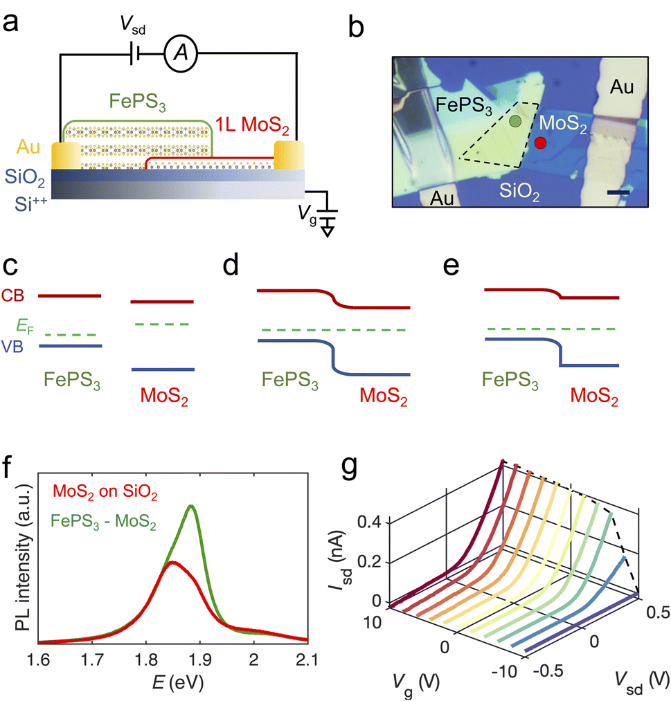 | ||
| Fig. 1 (a) Sketch for a device containing a multilayer FePS3/single-layer MoS2 heterostructure. (b) Optical microscopy image of a heterostructure device (device A). Scale bar: 10 µm. (c)–(e) Qualitative band alignment (c) before the two materials come into contact, (d) at the interface between the two materials in the in-plane lateral direction (lateral junction) and (e) at the interface between the two materials in the vertical direction (vertical junction). (f) PL spectra of device A taken at the single-layer MoS2 on top of SiO2 (red) and at the vertical heterojunction region (green), obtained at the corresponding color dots indicated in (b). PL spectra were taken using 532 nm laser excitation, with a power density of 65 µW µm−2. (g) Source–drain current–voltage characteristics as a function of the applied back-gate voltage for the same device. | ||
An energy band arrangement for this heterostructure is sketched in Fig. 1c, following the one provided in ref. 35. Single-layer MoS2 is a well-known, n-type 2D direct semiconductor with an estimated work function of ∼4.8 eV36 and a bandgap of 1.89 eV.2 Meanwhile, FePS3 has been reported to be a p-type indirect semiconductor with a work function around ∼4.9 eV35 and a bandgap of 1.23 eV33 (Fig. 1c). Based on this, a qualitative band alignment can be constructed, assuming a conventional bulk-like Shockley model (Fig. 1d). Electrostatic equilibrium at the interface requires the transfer of 1L-MoS2 free electron carriers to the available states in the valence band of FePS3. The bulk-like band alignment sketched in Fig. 1d holds for the lateral junction formed along the in-plane direction of the device, with depletion regions on both sides of the junction. However, for the region where the two materials overlap, a vertical p–n junction may form. In the vertical junction, a depletion layer is not possible at the single-layer MoS2 side, and the charge transfer at the interface results instead in a strong change in the doping level of the MoS2 monolayer (Fig. 1e).
The optical transmittance of 40-to-60 nm thick FePS3 flakes is ∼60% for visible wavelengths,33 which allows us to measure the PL emission of 1L-MoS2 underneath FePS3. Photoluminescence (PL) spectra, acquired from device A at the marked spots on Fig. 1b at the 1L-MoS2 on SiO2 and at the FePS3/1L-MoS2 heterostructure, respectively, are presented in Fig. 1f. In the heterostructure region, the PL emission of 1L-MoS2 is blue shifted and narrowed when compared to that of 1L-MoS2 directly deposited on SiO2. These changes in the PL emission arise from variations in the relative spectral weight of charged excitons, versus neutral ones. These variations have been attributed to changes in the free electron density in the 1L-MoS2 reflecting the amount of charge transferred between FePS3 and 1L-MoS2 upon contact (see ref. 35 and ESI S2†). Charge transfer between 1L-MoS2 and multilayer FePS3 was quantified by Ramos et al.35 as a function of the thickness of the FePS3 layer. Here, we find a qualitatively similar behaviour, even if, in this work, 1L-MoS2 is placed below FePS3, instead of above. The analysis of the PL data in Fig. S2† based on a mass action law model points also to a decrease in the charge carrier concentration of 1L-MoS2 when integrated in FePS3/1L-MoS2 heterostructures.
The optical characterization of FePS3/1L-MoS2 heterostructures suggests the formation of a junction with unusual properties, in agreement with ref. 35, which could reflect in their electrical photo-response. In the following, we present the optoelectronic characterization of the FePS3/1L-MoS2 heterostructure devices. Current–voltage (I–V) characteristics for the FePS3/1L-MoS2 device A are presented in Fig. 1g as a function of the applied back-gate voltage (Vg). These characteristics are compatible with the formation of a potential barrier at the interface between the materials, as sketched in Fig. 1e. At zero applied gate voltage (Vg = 0 V), the current (Isd) as a function of source–drain voltage (Vsd) follows the current rectifier behavior expected for a p–n diode (yellow curve in Fig. 1g). The application of a forward bias voltage (Vsd > 0 in Fig. 1g), promotes the diffusion of majority carriers across the barrier and the source–drain current grows exponentially with Vsd. On the other hand, the application of a reverse bias (Vsd < 0 in Fig. 1g) increases the potential barrier that blocks the passage of carriers through the barrier. Thus, the generated current (drift current) is almost negligible compared to that originated under forward bias.
Under the application of a back-gate voltage, the forward conduction of the device rapidly decreases for moderate values of Vg < 0, becoming negligible at Vg ∼ −10 V. A similar behavior has been reported for 1L-MoS2 field effect transistor devices at higher values of the applied Vg (see ref. 37 and Fig. S3†). This difference can be explained in terms of the proposed band alignment for the FePS3/1L-MoS2 vertical junction in Fig. 1e. Since 1L-MoS2 already has a reduced concentration of electrons due to their transfer to FePS3, a relatively small external electric field is enough to fully deplete the single-layer material and, consequently, to suppress conduction. On the contrary, the application of a positive gate voltage (Vg > 0), increases the free electron density in the 1L-MoS2, enhancing forward conduction.
The rectification ratio (RR), defined as the ratio between the forward and reverse currents, exhibits an increase as Vg decreases, reaching a maximum value of RR ∼ 750, at Vg = −2 V, for device A (RR ∼ 200 at Vg = −4 V for device B) and subsequently decreases for lower values of Vg (see Fig. S4†). The maximum RR values fall within the range reported for similar heterostructures in previous studies9,13,38–40 (see Table S2†).
When shining light to the entire device area (λ = 532 nm), a measurable photocurrent appears at zero and reverse bias, and grows with the excitation power (Fig. 2a). This photo-response is consistent with the characteristics of photovoltaic effects, where the separation of photoexcited electron–hole pairs is driven by the interfacial built-in electric field at the p–n heterojunction. A scanning photocurrent map at Vsd = 0 V reveals that the observed photo-response mainly arises from the region of vertical contact between both semiconducting materials (Fig. 2b). This suggests that the device's response upon illumination is governed by the built-in potential at the vertical junction. The photocurrent generated at the junction interface is not spatially homogeneous, likely due to the presence of adsorbates at the interface, retained during assembly of the device, or the formation of wrinkles during the transfer process. In contrast, no measurable photocurrent is observed in the non-overlapping region of the two van der Waals materials, nor at the lateral junctions or the metal–semiconductor contact areas. This suggests a negligible contribution from drift currents or charge separation induced by Schottky barriers to the photo-response observed under global illumination.
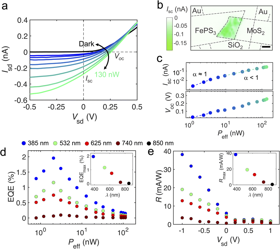 | ||
| Fig. 2 (a) Isd–Vsd characteristics of the FePS3/1L-MoS2 device shown in Fig. 1b (device A) upon dark and illumination conditions at different incident, effective, optical powers. (b) Scanning photocurrent map of device A, at Vsd = Vg = 0 V, obtained with an illumination spot of ∼1 µm diameter and Popt = 72 nW. Scale bar: 10 µm. (c) Short-circuit current and open-circuit voltage as a function of effective power, obtained from data in panel (a). (d) External quantum efficiency (EQE) as a function of effective power for different illumination wavelengths and for Vsd = 0 V (device B). Inset: maximum EQE versus incident wavelength obtained at Vsd = 0 V. (e) Maximum responsivity R obtained at different bias (device B). Inset: maximum responsivity versus incident wavelength obtained at Vsd = −1 V. | ||
To further characterize the response of the FePS3/MoS2 p–n photodiode, the photocurrent at zero external bias (short-circuit current, Isc) and photovoltage with no current flow (open-circuit voltage, Voc) are extracted from the Isd–Vsd curves measured as a function of increasing excitation power (Fig. 2a). For small incident powers, Isc displays a linear dependence on the effective power (Peff = Popt × Adevice/Aspot), whereas, for higher incident power values, it follows a power law (Isc ∝ Peffα) with α < 1 (Fig. 2c). This trend is commonly observed in similar systems, and it is attributed to a progressive saturation of the optical absorption of the device, due to the occupancy of photoexcited, in-gap, trapped states.4 Trapped carriers present larger lifetimes and low recombination probabilities, contributing to a decrease of the photocurrent generation efficiency. In the range where Isc is linear with power (Peff < 4 nW), the junction behaves according to the Shockley model, and Voc follows a semi-logarithmic dependence on Peff. From this dependence, we extract an ideality factor for the junction to be nid ≈ 2 (see ESI Section S5†), which describes a junction dominated by trap assisted recombination (Shockley–Read–Hall recombination mechanism).5,37,41
To evaluate the performance of FePS3/1L-MoS2 photodiodes, we calculate their external quantum efficiency (EQE) and responsivity (R), which are defined as the ratios of collected charge carriers to number of incident photons, EQE = hc × Iph/(Peff × e × λ), and photocurrent to illumination power, R = Iph/Peff, respectively. Power conversion efficiency is also estimated in the ESI Section S6.† In Fig. 2d, EQE is presented as a function of the incident effective power at different excitation wavelengths for device B at Vsd = 0 V. For all the wavelengths, EQE increases with the incident power, reaching a maximum value before a sudden decrease at higher excitation powers. This drop in EQE with increasing power is a consequence of the optical absorption saturation inferred from the trends observed previously for Isc and Voc in Fig. 2c (for device A). In the visible regime, for instance at λ = 532 nm, maxima EQE of ∼1.2% and R ∼ 5 mA W−1 are reached for device B at Peff = 2 nW and Vsd = 0 V (being Iph ∼ Isc). Similar values are obtained for other FePS3/1L-MoS2 devices (see for instance Fig. S6† for device A, showing maximum EQE ∼ 0.8% and R ∼ 3.5 mA W−1 under similar conditions).
As a function of the incident wavelength (see inset of Fig. 2d), the photo-response of the heterojunction drops dramatically for λ ≥ 740 nm, with nearly no EQE modulation with different incident effective powers, since these photon energies fall below the absorption threshold for single-layer MoS2 (Egap = 1.89 eV, λg = 656 nm). In contrast, the EQE of the system increases as the incident wavelength decrease (see inset in Fig. 2d). While the optical absorption of MoS2 monolayers diminishes rapidly for excitation wavelengths below 400 nm,42 previous works have reported a significant photon absorption in FePS3 flakes in the near UV regime.33,34 Compared to other van der Waals heterostructures, the photo-response efficiency of FePS3/1L-MoS2 is modest for visible wavelengths (see Tables S3–S5†). However, FePS3/1L-MoS2 devices present larger EQE for more energetic wavelengths, reaching a value of ∼2% for incident light towards the ultraviolet spectral region (Fig. 2d). Furthermore, the variation in the photo-responsivity with the applied source–drain voltage reveals a substantial increase in this efficiency for negative bias, displaying responsivity values up to R ∼ 40 mA W−1 at Vsd = −1 V for λ = 385 nm. These results indicate that FePS3/1L-MoS2 heterojunction devices can serve as efficient photodetectors when operated in the third quadrant (Vsd < 0 V), particularly for detection in the ultraviolet spectral region. This feature distinguishes them from other p–n van der Waals heterostructures containing single-layer TMDCs, which typically do not exhibit significant responsivities in the UV regime (see for example ref. 2, 4, 5, 9 and 43 and Table S5† for a comparison).
While the performance of van der Waals p–n devices containing single-layer TMDCs often tends to be smaller than those of their multilayer counterparts,7 they can offer distinct advantages stemming from the single-layer nature of their components. This is also the case of FePS3/1L-MoS2 heterostructures. Devices combining p-type FePS3 or FePSe3 with multilayer n-type TMDCs exhibit better performance than our devices (see for instance ref. 14 and 16 and Table S5† for a comparison). However, in FePS3/1L-MoS2 heterostructures, electrical photo-response appears together with a strong excitonic light emission (see Fig. 1f and 3), a characteristic which is absent in their bulk counterparts. The competition between these two phenomena cannot be easily explored in bulk, inorganic p–n junctions and has been explored for organic solar cells and semiconducting quantum well junctions.44,45 However, the interplay between PL and photocurrent generation remains rather unexplored in van der Waals p–n heterojunctions. Most heterojunctions composed of light-emitting single-layer TMDCs featuring a strong photovoltaic effect, typically present a significant PL quenching.4,27,46,47 In the following, we will explore the interplay between photocurrent generation and light emission in FePS3/1L-MoS2 van der Waals structures, taking advantage of the unusual phenomena coexistence in this system.
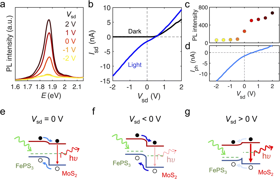 | ||
| Fig. 3 (a) PL emission of single-layer MoS2 composing the FePS3/1L-MoS2 heterojunction as a function of the applied bias voltage for a Peff = 180 µW and λ = 532 nm (device C). Spectra are acquired at the region where the two materials overlap with an illumination spot of ∼8 µm diameter and a collection spot of ∼16 µm diameter. (b) Isd–Vsd characteristics under dark (black) and illumination conditions (blue) for device C under same conditions (Peff = 180 µW, λ = 532 nm). (c) Maximum PL intensity as a function of the applied bias voltage, obtained from panel (a). (d) Photocurrent obtained from panel (b) as a function the applied bias voltage. (e–g) Sketch showing the competition between photocurrent generation and radiative recombination mechanisms for the FePS3–MoS2 p–n heterojunction for zero (e), negative (reverse) (f) and positive (forward) (g) applied bias voltages. | ||
Our results reveal a remarkable tunability of the PL emission from single-layer MoS2 as a function of the applied source–drain voltage (Vsd) across the heterojunction. In Fig. 3a, we present PL spectra acquired from an 8 µm diameter spot at the FePS3/1L-MoS2 vertical junction at different Vsd values (see Methods section for experimental details and Fig. S8† for results from a second device). A small change in bias voltage (in the order of Vsd ∼ 1 V) is enough to significantly tune (suppress or enhance) the PL intensity of single-layer MoS2 by more than ten times, a degree of tunability only reachable with large values of applied gate voltage.48 Regarding the interplay of PL and photocurrent, when Vsd is set to negative values (reverse bias), we observe a significant reduction in PL intensity (Fig. 3a and c), while achieving maximum photocurrent generation (Fig. 3b and d). As Vsd is swept from negative to positive values, the photocurrent decreases, and the PL raises. This trend continues until Vsd reaches ∼0.5 V, at which point the photocurrent approaches zero. For Vsd > 0.5 V (Fig. 3a and c), both photocurrent and PL emission increase (Fig. 3b and d).
Our findings can be qualitatively explained as follows: at Vsd = 0 V, the built-in potential at the heterointerface enables the dissociation of photoexcited electron–hole pairs, contributing to the measured photocurrent. The built-in potential generated at the FePS3/1L-MoS2 junction at zero bias may be small, due to the modest difference between the work function values of the two materials (∼100 meV).35 This may limit the photo-response efficiency, but, in turn, preserves the radiative recombination of excitons at the 1L-MoS2 side, allowing for the coexistence of photocurrent and PL emission (see sketch in Fig. 3e). At Vsd < 0 V (reverse bias), the potential barrier at the interface between the two semiconducting materials increases, favoring electron–hole pair dissociation over radiative recombination (Fig. 3f). On the contrary, when applying a forward bias (Vsd > 0), the potential difference across the junction is reduced. In this situation, the contribution of photoexcited carriers to the photocurrent at the junction decreases, promoting the recombination of electron–hole pairs at 1L-MoS2via radiative pathways (Fig. 3g). Once Vsd surpasses the open-circuit voltage (Voc ∼ 0.5 V in our case), no photocurrent is expected to arise at the junction. In fact, negligible photocurrent is observed in photocurrent maps at Vsd > 0.5 V (see Fig. S9†). The small increase of photocurrent at positive bias in Fig. 3d is likely related to photoconductivity and photogating effects. Nonetheless, this photocurrent does not seem to directly compete with the PL emission which continues to increase with Vsd > 0.5 V.
It is worth noting that the alignment sketched for Vsd > 0 V in Fig. 3g would, in principle, allow the transfer of both electrons and holes from 1L-MoS2 to FePS3 and potentially enable the emergence of electroluminescence, which has been observed for similar energy band arrangements in other van der Waals heterojunctions.43,49 However, the substantial increase of exciton radiative recombination suggests that the photocarrier transfer from 1L-MoS2 to FePS3 at positive bias must be small in our system, likely due to the momentum mismatch of MoS2 and FePS3 band structures.35 Besides, electroluminescence would not be expected to be a leading effect in an indirect gap semiconductor such as FePS3. The efficiency of non-radiative recombination processes, such as Auger50 or trap-assisted recombination,5,37,41 might also vary with the applied bias, and could explain further details of the photocurrent and photoluminescence behaviour, for example, the saturation in the PL increase for Vsd > 1 V (see ESI S13†).
Finally, we found that the photo-response of the FePS3/1L-MoS2 p–n diodes can be modulated by applying a back-gate voltage (Fig. 4a and S10†). In terms of the incident power, we distinguish two different regimes for photocurrent generation as a function of Vg. First, we observed that for low excitation power (Peff ∼ 10 nW) the photocurrent – and, thus, the responsivity – at zero and reverse bias (Vsd ≤ 0) increases towards positive values of Vg (Fig. 4b), as the built-in potential at the junction increases. Conversely, a negative gate voltage would lower the potential barrier at the junction and justify the decrease of photocurrent for negative values of Vg observed in Fig. 4b. It is worth noting that the modulation of the photocurrent at Vg > 0 is smaller in our heterostructures compared to other systems, such as BP/1L-MoS2.9 This difference could be due to the higher resistance of FePS3 limiting the overall current flowing through the device.
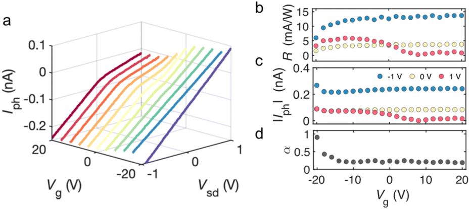 | ||
| Fig. 4 (a) Photocurrent (Iph = Ilight − Idark) as a function of Vsd and for different Vg, measured upon illumination with λ = 532 nm and Peff = 95 nW for device B. (b) Responsivity as a function of applied gate voltage for negative, zero and positive bias voltage, obtained at Peff ∼ 10 nW. (c) Photocurrent as a function of Vg, for negative, zero and positive bias voltage, and for Peff ∼ 100 nW. (d) Exponent α from photocurrent dependence on power (Iph = N × Peff)α, measured at Vsd = 0 V, within the power range where photo-gating effects dominate (Peff = 10–50 nW). | ||
Typically, the diode photocurrent under forward bias is negligible in comparison to the reverse bias regime. While this is the case for Vg > 0, photocurrent generation in forward bias remarkably increases for Vg < 0 in our heterojunctions (Fig. 4b) and the external gate voltage can effectively switch the forward photocurrent generation on and off. Furthermore, for Vg < 0 and Vsd > 0, FePS3/1L-MoS2 photodiodes exhibit higher photocurrents than those obtained at zero and positive bias (Fig. 4b) and, thus, can operate as photodetectors both under reverse and forward configurations.
In the case of higher incident powers (Peff ∼ 100 nW), Iph behaves similarly to the low-power case within the range between Vg = −10 V to + 20 V (Fig. 4c). However, an interesting change in this trend appears in Fig. 4c for Vg < −10 V, with a sudden increase of Iph. To understand this behavior, we have analyzed the power law dependence of photocurrent on excitation power at zero bias and within the power range of 10 to 50 nW. In this regime, at Vg = 0 V, the photocurrent follows a power law expression, Iph = N × Pα with α < 1 (Fig. 2c), indicating relevant contributions from photo-gating to photocurrent generation.51 Photo-gating effects have been extensively reported for both 1L-MoS2 and FePS3 due to the presence of charge-trap defects in both materials. Hence, the presence of photo-gating effects in the heterostructure is expected. For positive and small negative values of Vg, α exhibits values well below unity (α ≪ 1), suggesting that photo-gating effects strongly influence photocurrent generation (Fig. 4d). However, for Vg < −10 V, α increases significantly indicating that photo-gating effects cease to dominate the photocurrent generation at larger negative gate voltages. This occurs in the same range of values of Vg at which Iph increases (Fig. 4c) and the forward conduction in dark is suppressed (Fig. 1g). Therefore, our results suggest that carrier depletion in 1L-MoS2 entails a reduction in available trap states at the junction interface, resulting in improved photocurrent generation performance.
Conclusions
In summary, heterostructures built out from multilayer FePS3 and single-layer MoS2 (in short FePS3/1L-MoS2) constitute p–n photodiodes characterized by the coexistence of broadband electrical photo-response and robust excitonic emission. These unique features stem from the single-layer nature of MoS2, the absorption properties of FePS3, and the electronic properties of their interface. Compared to other devices containing single-layer TMDCs, FePS3/1L-MoS2 junctions present improved efficiency rates for UV photodetection. Moreover, both photocurrent and photoluminescence emission present a remarkable tunability under small, applied voltages, which likely arise from the band alignment at the interface. This exceptional tunability allows for precise control of the photoluminescence emission through minor adjustments to the voltage across the junction. Consequently, FePS3/1L-MoS2 heterostructures hold promise for gaining further insights into the competition between carrier dissociation and recombination at van der Waals interfaces, leading to the design of devices with enhanced performance. Furthermore, these heterostructures exemplify how varying alignments at different material interfaces can introduce additional functionality, tunability, and versatility to van der Waals devices.Materials and methods
Crystal synthesis
Pristine FePS3 crystals were grown via chemical vapor transport (CVT), using iodine as a transport agent,52 whereas bulk MoS2 was provided commercially from SPI Supplies.Heterostructure fabrication
Thin flakes of FePS3 and MoS2 were obtained through the Scotch tape method from their bulk crystals and transferred onto viscoelastic substrates, polydimethylsiloxane (PDMS), for optical inspection under a microscope. Once the ideal flakes were identified (proper thickness and geometry), the dry transfer method53 was employed to stamp deterministically the desired flakes onto SiO2/Si++ (270 nm oxide layer) substrates with prepattern Ti/Au contacts. The mechanical exfoliation of FePS3 crystals and the heterostructure stacking were carried out inside a glovebox inert Ar atmosphere. Single layer MoS2 flakes were identified by micro-reflectance spectroscopy54 and corroborated by Raman spectroscopy (Fig. S11†), using a Jasco NRS-5100 microscope. The thickness of the FePS3 layer (40–60 nm) was determined by micro-reflectance spectroscopy33 after device fabrication (see ESI Section S1†).Micro-photoluminescence spectroscopy, three-terminal electrical measurements and scanning photocurrent map
The three types of experiments were carried out in a home-built equipment, provided of a confocal microscope and electrical contacts, to simultaneously study the interplay between photoluminescence and photoconductivity in the devices. Devices were mounted onto a motorized platform with movement along the x–y directions, allowing to run photocurrent maps with sub-micrometer step resolution. The excitation CW laser used for simultaneous photoluminescence and photocurrent measurements was a RLTMGL-532-500-1 (Roithner Lasertechnik), with an excitation line at 532 nm, fiber-coupled for a better integration in the setup. LED sources were used for other excitation wavelengths. For scanning photocurrent maps, a spot diameter of about 1 µm was used, whereas for opto-electronic transport measurements in Fig. 1, 2 and 4 a global illumination was employed (spot diameter ∼ 80 µm). For photoluminescence spectra acquisition the excitation spot had ∼8 µm of diameter and was centred on the vertical junction. Light emission was collected from a ∼16 µm diameter spot. A Keithley 2450 sourcemeter was employed for the electrical measurements. Devices were kept in Ar atmosphere and characterized within an average time of 1–2 weeks, to avoid degradation upon air exposure.33Author contributions
Maria Ramos: device fabrication and characterization, data curation, formal analysis, visualization, writing – original draft. Marcos Gadea: device fabrication and characterization, data curation, formal analysis, writing – original draft. Samuel Mañas-Valero: material growth, device fabrication. Carla Boix-Constant: material growth, device fabrication. Eudomar Henríquez-Guerra: characterization. María Ángeles Díaz-García: validation, writing – review & editing. Eugenio Coronado: resources, validation, writing – review & editing. M. Reyes Calvo: conceptualization, formal analysis, funding acquisition, supervision, visualization, writing – original draft.Conflicts of interest
There are no conflicts to declare.Acknowledgements
The authors thank J. J. Baldoví and J. Canet-Ferrer for fruitful discussion. The authors acknowledge funding from Generalitat Valenciana through grants MFA/2022/045 and MFA/2022/050, IDIFEDER/2020/005, IDIFEDER/2021/016, PROMETEO Program and PO FEDER Program, the APOSTD/2020/249 fellowship for M. R., and support from the Plan Gen-T of Excellence for M. R. C. (CideGenT2018004); from the Spanish MCINN through grants PLASTOP PID2020-119124RB-I00, 2D-HETEROS PID2020-117152RB-100, and Excellence Unit “María de Maeztu” CEX2019-000919-M; and from the European Union (ERC AdG Mol-2D 788222).References
- D. A. Neamen, Semiconductor Physics and Devices: Basic Principles, McGraw-Hill, Boston, 3rd edn, 2003 Search PubMed.
- R. Frisenda, A. J. Molina-Mendoza, T. Mueller, A. Castellanos-Gomez and H. S. J. van der Zant, Chem. Soc. Rev., 2018, 47, 3339 RSC.
- R. Liu, F. Wang, L. Liu, X. He, J. Chen, Y. Li and T. Zhai, Small Struct., 2021, 2, 2000136 CrossRef CAS.
- M. M. Furchi, A. Pospischil, F. Libisch, J. Burgdörfer and T. Mueller, Nano Lett., 2014, 14, 4785 CrossRef CAS PubMed.
- C. H. Lee, G. H. Lee, A. M. van der Zande, W. Chen, Y. Li, M. Han, X. Cui, G. Arefe, C. Nuckolls, T. F. Heinz, J. Guo, J. Hone and P. Kim, Nat. Nanotechnol., 2014, 9, 676 CrossRef CAS PubMed.
- A. Pospischil, M. M. Furchi and T. Mueller, Nat. Nanotechnol., 2014, 9, 257 CrossRef CAS PubMed.
- M. M. Furchi, F. Höller, L. Dobusch, D. K. Polyushkin, S. Schuler and T. Mueller, npj 2D Mater. Appl., 2018, 2, 3 CrossRef.
- J. Wong, D. Jariwala, G. Tagliabue, K. Tat, A. R. Davoyan, M. C. Sherrott and H. A. Atwater, ACS Nano, 2017, 11, 7230 CrossRef CAS PubMed.
- Y. Deng, Z. Luo, N. J. Conrad, H. Liu, Y. Gong, S. Najmaei, P. M. Ajayan, J. Lou, X. Xu and P. D. Ye, ACS Nano, 2014, 8, 8292 CrossRef CAS PubMed.
- P. Wu, L. Ye, L. Tong, P. Wang, Y. Wang, H. Wang, H. Ge, Z. Wang, Y. Gu, K. Zhang, Y. Yu, M. Peng, F. Wang, M. Huang, P. Zhou and W. Hu, Light: Sci. Appl., 2022, 11, 6 CrossRef CAS PubMed.
- M. Long, E. Liu, P. Wang, A. Gao, H. Xia, W. Luo, B. Wang, J. Zeng, Y. Fu, K. Xu, W. Zhou, Y. Lv, S. Yao, M. Lu, Y. Chen, Z. Ni, Y. You, X. Zhang, S. Qin, Y. Shi, W. Hu, D. Xing and F. Miao, Nano Lett., 2016, 16, 2254 CrossRef CAS PubMed.
- K. Zhang, T. Zhang, G. Cheng, T. Li, S. Wang, W. Wei, X. Zhou, W. Yu, Y. Sun, P. Wang, D. Zhang, C. Zeng, X. Wang, W. Hu, H. J. Fan, G. Shen, X. Chen, X. Duan, K. Chang and N. Dai, ACS Nano, 2016, 10, 3852 CrossRef CAS PubMed.
- X. Jiang, M. Zhang, L. Liu, X. Shi, Y. Yang, K. Zhang, H. Zhu, L. Chen, X. Liu, Q. Sun and D. W. Zhang, Nanophotonics, 2020, 9, 2487 CrossRef CAS.
- J. Duan, P. Chava, M. Ghorbani-Asl, Y. Lu, D. Erb, L. Hu, A. Echresh, L. Rebohle, A. Erbe, A. V. Krasheninnikov, M. Helm, Y. J. Zeng, S. Zhou and S. Prucnal, ACS Appl. Mater. Interfaces, 2022, 14, 11927 CrossRef CAS PubMed.
- Y. Wang, Y. Tang, H. Li, Z. Yang, Q. Zhang, Z. He, X. Huang, X. Wei, W. Tang, W. Huang and Z. Wu, ACS Photonics, 2021, 8, 2256 CrossRef CAS.
- M. Long, Z. Shen, R. Wang, Q. Dong, Z. Liu, X. Hu, J. Hou, Y. Lu, F. Wang, D. Zhao, F. Ding, Y. Tu, T. Han, F. Li, Z. Zhang, X. Hou, S. Wang and L. Shan, Adv. Funct. Mater., 2022, 32, 2204230 CrossRef CAS.
- Y. Xin, X. Wang, Z. Chen, D. Weller, Y. Wang, L. Shi, X. Ma, C. Ding, W. Li, S. Guo and R. Liu, ACS Appl. Mater. Interfaces, 2020, 12, 15406 CrossRef CAS PubMed.
- H. Gao, C. Du, J. Sun, J. Zhang, J. Leng, J. Li, W. Wang and K. Li, Mater. Today Commun., 2023, 35, 105959 CrossRef CAS.
- F. Withers, O. Del Pozo-Zamudio, A. Mishchenko, A. P. Rooney, A. Gholinia, K. Watanabe, T. Taniguchi, S. J. Haigh, A. K. Geim, A. I. Tartakovskii and K. S. Novoselov, Nat. Mater., 2015, 14, 301 CrossRef CAS PubMed.
- K. S. Novoselov, A. Mishchenko, A. Carvalho and A. H. Castro Neto, Science, 2016, 353, aac9439 CrossRef CAS PubMed.
- J. Y. Lim, M. Kim, Y. Jeong, K. R. Ko, S. Yu, H. G. Shin, J. Y. Moon, Y. J. Choi, Y. Yi, T. Kim and S. Im, npj 2D Mater. Appl., 2018, 2, 1 CrossRef CAS.
- L. Gao, Small, 2017, 13, 1603994 CrossRef PubMed.
- T. U. Tran, D. A. Nguyen, N. T. Duong, D. Y. Park, D. H. Nguyen, P. H. Nguyen, C. Park, J. Lee, B. W. Ahn, H. Im, S. C. Lim and M. S. Jeong, Appl. Mater. Today, 2022, 26, 101285 CrossRef.
- T. Mueller and E. Malic, npj 2D Mater. Appl., 2018, 2, 29 CrossRef.
- K. F. Mak, C. Lee, J. Hone, J. Shan and T. F. Heinz, Phys. Rev. Lett., 2010, 105, 136805 CrossRef PubMed.
- A. Splendiani, L. Sun, Y. Zhang, T. Li, J. Kim, C. Y. Chim, G. Galli and F. Wang, Nano Lett., 2010, 10, 1271 CrossRef CAS PubMed.
- J. Yuan, S. Najmaei, Z. Zhang, J. Zhang, S. Lei, P. M. Ajayan, B. I. Yakobson and J. Lou, ACS Nano, 2015, 9, 555 CrossRef CAS PubMed.
- Y. Wang, J. C. Kim, Y. Li, K. Y. Ma, S. Hong, M. Kim, H. S. Shin, H. Y. Jeong and M. Chhowalla, Nature, 2022, 610, 61 CrossRef PubMed.
- A. Zavabeti, P. Aukarasereenont, H. Tuohey, N. Syed, A. Jannat, A. Elbourne, K. A. Messalea, B. Y. Zhang, B. J. Murdoch, J. G. Partridge, M. Wurdack, D. L. Creedon, J. van Embden, K. Kalantar-Zadeh, S. P. Russo, C. F. McConville and T. Daeneke, Nat. Electron., 2021, 4, 277 CrossRef CAS.
- X. Zhang, H. Yu, W. Tang, X. Wei, L. Gao, M. Hong, Q. Liao, Z. Kang, Z. Zhang and Y. Zhang, Adv. Mater., 2022, 34, 2109521 CrossRef CAS PubMed.
- Y. Xiong, D. Xu, Y. Feng, G. Zhang, P. Lin and X. Chen, Adv. Mater., 2023, 35, 2206939 CrossRef CAS PubMed.
- Y. Gao, S. Lei, T. Kang, L. Fei, C. L. Mak, J. Yuan, M. Zhang, S. Li, Q. Bao, Z. Zeng, Z. Wang, H. Gu and K. Zhang, Nanotechnology, 2018, 29, 244001 CrossRef PubMed.
- M. Ramos, F. Carrascoso, R. Frisenda, P. Gant, S. Mañas-Valero, D. L. Esteras, J. J. Baldoví, E. Coronado, A. Castellanos-Gomez and M. R. Calvo, npj 2D Mater. Appl., 2021, 5, 1 CrossRef.
- R. Brec, D. M. Schleich, G. Ouvrard, A. Louisy and J. Rouxel, Inorg. Chem., 1979, 18, 1814 CrossRef CAS.
- M. Ramos, F. Marques-Moros, D. L. Esteras, S. Mañas-Valero, E. Henríquez-Guerra, M. Gadea, J. J. Baldoví, J. Canet-Ferrer, E. Coronado and M. R. Calvo, ACS Appl. Mater. Interfaces, 2022, 14, 33482 CrossRef CAS PubMed.
- M. Tamulewicz, J. Kutrowska-Girzycka, K. Gajewski, J. Serafińczuk, A. Sierakowski, J. Jadczak, L. Bryja and T. P. Gotszalk, Nanotechnology, 2019, 30, 245708 CrossRef CAS PubMed.
- M. M. Furchi, D. K. Polyushkin, A. Pospischil and T. Mueller, Nano Lett., 2014, 14, 6165 CrossRef CAS PubMed.
- A. J. Molina-Mendoza, E. Giovanelli, W. S. Paz, M. A. Niño, J. O. Island, C. Evangeli, L. Aballe, M. Foerster, H. S. J. Van Der Zant, G. Rubio-Bollinger, N. Agraït, J. J. Palacios, E. M. Pérez and A. Castellanos-Gomez, Nat. Commun., 2017, 8, 14409 CrossRef CAS PubMed.
- X. Wang, L. Huang, Y. Peng, N. Huo, K. Wu, C. Xia, Z. Wei, S. Tongay and J. Li, Nano Res., 2016, 9, 507 CrossRef CAS.
- S. A. Svatek, E. Antolin, D. Y. Lin, R. Frisenda, C. Reuter, A. J. Molina-Mendoza, M. Muñoz, N. Agraït, T. S. Ko, D. P. De Lara and A. Castellanos-Gomez, J. Mater. Chem. C, 2017, 5, 854 RSC.
- W. Shockley and W. T. Read, Phys. Rev., 1952, 87, 835 CrossRef CAS.
- A. Castellanos-Gomez, J. Quereda, H. P. Meulen, H. P. van der Meulen, N. Agraït and G. Rubio-Bollinger, Nanotechnology, 2016, 27, 115705 CrossRef PubMed.
- R. Cheng, D. Li, H. Zhou, C. Wang, A. Yin, S. Jiang, Y. Liu, Y. Chen, Y. Huang and X. Duan, Nano Lett., 2014, 14, 5590 CrossRef CAS PubMed.
- J. Barnes, E. S. M. Tsui, K. W. J. Barnham, S. C. McFarlane, C. Button and J. S. Roberts, J. Appl. Phys., 1997, 81, 892 CrossRef CAS.
- S. J. Oh, J. Kim, J. M. Mativetsky, Y. L. Loo and C. R. Kagan, ACS Appl. Mater. Interfaces, 2016, 8, 28743 CrossRef CAS PubMed.
- Y. Gong, J. Lin, X. Wang, G. Shi, S. Lei, Z. Lin, X. Zou, G. Ye, R. Vajtai, B. I. Yakobson, H. Terrones, M. Terrones, B. K. Tay, J. Lou, S. T. Pantelides, Z. Liu, W. Zhou and P. M. Ajayan, Nat. Mater., 2014, 13, 1135 CrossRef CAS PubMed.
- W. Yang, H. Kawai, M. Bosman, B. Tang, J. Chai, W. L. Tay, J. Yang, H. L. Seng, H. Zhu, H. Gong, H. Liu, K. E. J. Goh, S. Wang and D. Chi, Nanoscale, 2018, 10, 22927 RSC.
- X. Zhang, H. Nan, S. Xiao, X. Wan, Z. Ni, X. Gu and K. Ostrikov, ACS Appl. Mater. Interfaces, 2017, 9, 42121 CrossRef CAS PubMed.
- X. Zong, H. Hu, G. Ouyang, J. Wang, R. Shi, L. Zhang, Q. Zeng, C. Zhu, S. Chen, C. Cheng, B. Wang, H. Zhang, Z. Liu, W. Huang, T. Wang, L. Wang and X. Chen, Light: Sci. Appl., 2020, 9, 114 CrossRef CAS PubMed.
- P. D. Cunningham, K. M. McCreary and B. T. Jonker, J. Phys. Chem. Lett., 2016, 7, 5242 CrossRef CAS PubMed.
- T. U. Tran, D. A. Nguyen, N. T. Duong, D. Y. Park, D. H. Nguyen, P. H. Nguyen, C. Park, J. Lee, B. W. Ahn, H. Im, S. C. Lim and M. S. Jeong, Appl. Mater. Today, 2022, 26, 101285 CrossRef.
- M. Šiškins, M. Lee, S. Mañas-Valero, E. Coronado, Y. M. Blanter, H. S. J. van der Zant and P. G. Steeneken, Nat. Commun., 2020, 11, 2698 CrossRef PubMed.
- A. Castellanos-Gomez, M. Buscema, R. Molenaar, V. Singh, L. Janssen, H. S. J. van der Zant and G. A. Steele, 2D Mater., 2014, 1, 011002 CrossRef CAS.
- R. Frisenda, Y. Niu, P. Gant, A. J. Molina-Mendoza, R. Schmidt, R. Bratschitsch, J. Liu, L. Fu, D. Dumcenco, A. Kis, D. P. D. Lara and A. Castellanos-Gomez, J. Phys. D: Appl. Phys., 2017, 50, 074002 CrossRef.
Footnotes |
| † Electronic supplementary information (ESI) available. See DOI: https://doi.org/10.1039/d3na01134h |
| ‡ Equal contribution. |
| This journal is © The Royal Society of Chemistry 2024 |