 Open Access Article
Computational approaches to enhance charge transfer and stability in TPBi–(PEA)2PbI4 perovskite interfaces through molecular orientation optimization†
Syed Muhammad Kazim Abbas
Naqvi
 ab,
Yanan
Zhu
 *b,
Hui
Long
bc,
Zahid
Nazir
b,
Roman B.
Vasiliev
 c,
Olga
Kulakovich
 d and
Shuai
Chang
 *b
*b
aSchool of Materials Science & Engineering, Beijing Institute of Technology, Beijing 100081, China
bPlatform for Applied Nanophotonics, Faculty of Materials Science, Shenzhen MSU-BIT University, Shenzhen 518115, China. E-mail: zhuyn@smbu.edu.cn; schang@smbu.edu.cn
cDepartment of Materials Science, Department of Chemistry, Lomonosov Moscow State University, Moscow 119991, Russia
dInstitute of Physics of the National Academy of Sciences of Belarus, Minsk 220072, Belarus
First published on 1st July 2024
Abstract
The optimization of material interfaces is crucial for the performance and longevity of optoelectronic devices. This study focuses on 1,3,5-tris(1-phenyl-1H-benzimidazol-2-yl)benzene (TPBi), a key component in perovskite devices known for its efficient charge transfer capabilities. We investigate the TPBi–(PEA)2PbI4 heterostructure interfaces to enhance device durability by optimizing interfacial properties. Our findings reveal that those specific TPBi orientations – at 15 and 30 degrees – ensure strong electronic coupling between TPBi and (PEA)2PbI4, which improves stability at these interfaces. Furthermore, orientations at 15 and 60 degrees markedly enhance charge transfer kinetics, indicating reduced recombination rates and potentially increased efficiency in optoelectronic devices. These results not only underscore the importance of molecular orientation in perovskite devices but also open new avenues for developing more stable and efficient hybrid materials in optoelectronic applications.
Introduction
The field of photovoltaics has witnessed notable advancements, especially with the advent of three-dimensional (3D) hybrid halide perovskites. These materials offer adjustable band gaps, enhanced electron–hole diffusion lengths, low recombination rates, and cost-effective manufacturing. However, challenges such as device degradation due to environmental factors like oxygen and moisture persist.1–6 In the face of these challenges, researchers have turned their attention to two-dimensional (2D) hybrid perovskites, inspired by the success of various 2D materials like transition metal dichalcogenides,7,8 black phosphorus,9 boron nitride (BN), and graphene.10 These ultrathin 2D perovskites are currently being explored for applications in optoelectronics, including LEDs, FETs, and photodetectors. Building on experimental progress, significant theoretical investigations have delved into the electronic structures and optical characteristics of 2D perovskites. These studies suggest their high efficiency in absorption and photovoltaic applications, with performance variations based on their dimensional properties and inherent characteristics.11–16 Notably, studies exemplify the potential of 2D perovskites, as demonstrated by Yang et al., who synthesized single-crystalline 2D perovskites using a colloidal method, confirming their suitability for optoelectronic detection devices.17–20In scientific discourse, there's an ongoing debate about the most effective use of 2D layered perovskites: should they be optimized for photovoltaic solar cells or optoelectronic detection devices? This study aims to clarify this issue, specifically focusing on the unique 2D layered phenylethylammonium (PEA) lead halide perovskite (PEA)2PbI4. The unique nature of 2D layered PEA lead halide perovskite stems from its distinctive structural and optoelectronic properties, setting it apart from other materials within the perovskite family. Structurally, PEA lead halide perovskite adopts a layered configuration, with organic phenylethylammonium cations sandwiched between inorganic lead halide layers. This 2D arrangement contrasts with the 3D structure commonly found in traditional perovskite materials, imparting flexibility and tunability to its properties. The incorporation of organic cations within the inorganic framework allows for precise control over its electronic band structure. Regarding optoelectronic properties, PEA perovskites exhibit intriguing behaviours such as tunable band gaps, strong light–matter interactions, and enhanced stability compared to their 3D counterparts.21–24 This organic–inorganic hybrid nature enables them to serve as promising candidates for various optoelectronic applications.25,26 Additionally, PEA lead halide perovskites demonstrate improved stability compared to purely inorganic perovskite counterparts, attributed to the mitigating effects of organic cations on defects and structural instabilities. Their enhanced stability contributes to improved material durability and performance under diverse environmental conditions. Furthermore, PEA perovskites are typically solution-processable, allowing seamless integration into thin-film optoelectronic devices through scalable and cost-effective manufacturing techniques. This solution processability, combined with their favourable optoelectronic properties, renders PEA perovskites attractive for large-scale applications such as solar cells, LEDs, and photodetectors.25,27,28
Through first-principle calculations, we meticulously examine the geometric and electronic properties of (PEA)2PbI4, paying particular attention to its charge transport characteristics and binding energy. Our primary objective is to develop a theoretical framework that offers valuable insights and potentially bridges the gap in the ongoing debate about the most advantageous applications of 2D perovskites in photovoltaics and optoelectronics. 2D perovskite materials, characterized by the chemical formula A2BX4, consist of stacked octahedral metal-halide (B–X) monolayers and are separated by long-chain organic molecules (A) to maintain charge balance.16,29,30 A notable feature of 2D hybrid perovskites, which sets them apart from their 3D counterparts, is their enhanced stability.31,32 This stability is attributed mainly to the substantial van der Waals (vdW) interactions between the organic cations and inorganic anions, which help maintain the integrity of the 2D crystal structure. These materials also offer several distinct advantages, such as molecular-scale self-assembly, solution processability, excellent film formation capabilities, and remarkable optical properties characterized by extensive carrier diffusion lengths.33,34 However, challenges remain since the inclusion of an organic insulating layer in 2D perovskites can widen the energy band gap, increase exciton binding energy, and reduce optical absorption. These factors collectively present hurdles in achieving high energy conversion efficiency in 2D perovskite solar cells.23,35,36 To improve the electronic structures and carrier transport properties of 2D perovskite, including aspects such as mobility, recombination, and the impact of molecular orientation on carrier properties, the design of vdW heterostructures37,38 has been identified as a promising strategy. This development expands our ability to tailor specific electronic and optoelectronic properties.39,40 However, there remains a notable gap in both theoretical and experimental research regarding the photoelectric properties of vdW heterostructures that incorporate 2D perovskites, particularly when combined with TPBi (1,3,5-tris(1-phenyl-1H-benzimidazol-2-yl)benzene). Critical aspects, such as the energy band gap and band offsets within the TPBi–(PEA)2PbI4 heterostructure, are yet to be fully explored despite their crucial importance in semiconductor heterostructure design.
A unique feature of TPBi is its remarkable orientation flexibility,41 which can be skillfully leveraged to tailor photovoltaic properties.42,43 The orientation of TPBi molecules within a device significantly affects charge transport characteristics, providing a means to mitigate the degradation of the emissive layer and improve overall device performance.44,45 This aspect is particularly vital given that crystal orientation is a crucial factor in the performance of multi-layer optoelectronic devices.46 Furthermore, the ability to manipulate molecular orientation offers a promising pathway to enhance charge carrier transfer within the charge transport layers. Such dynamics have the exciting potential to increase device efficiency, carrier mobility, and overall lifespan, marking a significant advancement towards the ideal optoelectronic device. The focal point of our research is the manipulation mechanism of molecular orientation at the interface between TPBi and perovskite materials. This aspect is instrumental in determining the efficiency, stability, and overall longevity of optoelectronic devices, and it plays a pivotal role in their potential for commercialization. Different molecular orientations can introduce specific changes in charge transfer properties,47 a factor that could lead to the emergence of both energetic and positional disorders. These disorders have a significant impact on the characteristics of charge transport within the device.48
vdW interactions play a critical role in determining the orientations of TPBi molecules at the interface between TPBi and (PEA)2PbI4 perovskite materials. These interactions encompass both attractive forces, such as dispersion forces, and repulsive forces arising from steric effects.49 The strength of these interactions is influenced by factors like molecular shape, size, and the distance between molecules. At the TPBi–(PEA)2PbI4 perovskite materials, London dispersion forces come into play due to the temporary fluctuations in electron cloud distributions, leading to attractive interactions.50 The alignment of TPBi and (PEA)2PbI4 perovskite materials, such as molecules in a way that minimizes repulsion and maximizes attractive forces, is dependent on the molecular geometry and electron distribution of each component. Achieving compatibility in molecular shape and electron density distribution optimizes vdW interactions, thereby reducing potential energy and facilitating favourable molecular orientations. This optimized arrangement enhances the efficiency of charge transfer and binding energy at the TPBi(PEA)2PbI4 perovskite materials.51,52 To precisely manipulate TPBi orientations in laboratory experiments, specific techniques are employed, including vapour deposition conditions that can be finely tuned to control TPBi deposition and interactions during the process. Controlled annealing, where temperature parameters are adjusted, allows for the reorganization of TPBi molecules to enhance interactions. Surface modification techniques, which involve altering either the substrate or the TPBi layer, can also be utilized to strengthen interactions. Leveraging van der Waals forces, the layer-by-layer assembly method creates well-defined interfaces. Additionally, external fields can induce the reorientation of TPBi molecules after fabrication to achieve preferred alignments.53–57 However, these endeavours are not without challenges. The properties of the substrate can influence the nature of forces and interactions taking place. The tendency of TPBi molecules to aggregate can impact the deposition process and subsequent interactions, necessitating careful consideration. Balancing thermal stability during annealing procedures is crucial to prevent molecular degradation and optimize interactions. Beyond van der Waals interactions, other forces such as electrostatic interactions and hydrogen bonding should be taken into account. Furthermore, the broader context of environmental impact and reproducibility in large-scale production introduces additional layers of complexity. Regarding the impact of molecular orientation on device performance, our ongoing experimental investigations aim to elucidate the correlation between molecular orientation and the efficiency, stability, and performance of perovskite solar cells. Preliminary results suggest that variations in TPBi molecular orientation can significantly affect charge transport characteristics, recombination dynamics, and overall device performance. For instance, devices with vertically aligned TPBi molecules exhibit enhanced charge extraction efficiency and reduced charge recombination rates, leading to improved photovoltaic performance and stability compared to devices with randomly oriented TPBi layers.
In our previous research,58 we concentrated on studying TPBi–FAPbI3 heterostructures, highlighting the critical role of TPBi molecular orientation in affecting electronic band gaps and interfacial interactions. Building upon these findings, our current work focuses on TPBi–(PEA)2PbI4 heterostructures, delving into their unique electronic properties and charge transfer behaviours. This shift marks our continued dedication to broadening the scope of perovskite heterostructure research and deepening our understanding of this distinct system. Employing density functional theory (DFT), our latest study investigates TPBi–(PEA)2PbI4 vdW heterostructures By manipulating the orientations of TPBi molecules, we achieve tunable band gaps, enhanced charge transport, and improved interfacial stability. These findings open promising avenues for developing low-dimensional optoelectronic devices. Supporting our theoretical predictions, recent experimental work59 has successfully validated the complex interactions between TPBi and perovskite materials, setting an exciting groundwork for future advancements in optoelectronic device design.
Theoretical methods
In this study, ab initio calculations were conducted to examine the impact of different orientations on the charge transfer characteristics at the interface and binding energy of the TPBi–(PEA)2PbI4 heterostructure. These computational simulations were carried out employing the projector augmented wave (PAW) method within the framework of the Vienna ab initio simulation package (VASP) software.60 The molecular configuration of TPBi in isolation was constructed utilizing the Avogadro software.61 Subsequently, structural optimization of TPBi was conducted, with the Perdew–Burke–Ernzerhof (PBE) exchange-correlation function,62 grounded in the generalized gradient approximation (GGA),63 implemented via the Gaussian 09 (ref. 64) software package to obtain the converged geometry. Regarding the (PEA)2PbI4 structure, a relaxation procedure was implemented within the VASP environment, guaranteeing its aptness for the assembly of the intended heterostructures. Density functional theory (DFT)65 calculations were performed utilizing the B3LYP functional66 along with a 6–31G(d,p) basis set.67Results and discussion
At the TPBi–(PEA)2PbI4 interface, we examined TPBi–(PEA)2PbI4 heterostructures with six different TPBi orientations. Initial distances between the nearest TPBi atom and (PEA)2PbI4 atom were 2 Å due to vdW interactions. However, these distances exhibited variations after relaxation, as outlined in Table S1.† This interaction induced structural distortion at the (PEA)2PbI4 surface, as shown in Fig. 1. Using optimized structures, we analysed binding energy, electron density, charge distribution, and charge transfer parameters. The detailed results are provided in the ESI Section,† with a visual representation of binding energy variations presented in Trend Fig. S1.†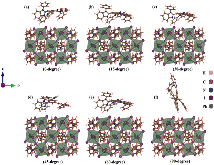 | ||
| Fig. 1 Relaxed TPBi–(PEA)2PbI4 heterostructures with (a) 0-degree, (b) 15-degree, (c) 30-degree, (d) 45-degree, (e) 60-degree, (f) 90-degree orientation of TPBi. | ||
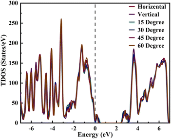
We conducted a comprehensive analysis of the density of states (DOS) (Fig. 2) and projected density of states (PDOS) (Fig. 3). DOS analysis revealed that varied TPBi orientations influence the electronic bandgap. Examining DOS profiles allowed the identification of additional electronic states resulting from interface hybridization in different orientations. Total density of state (TDOS) plots for various TPBi orientations (0-degree, 15-degree, 30-degree, 45-degree, 60-degree, and 90-degree) are shown in Fig. S2(a–f).† These plots offer side-by-side comparisons of TDOS profiles of (PEA)2PbI4 and the specific TPBi–(PEA)2PbI4 heterostructure, facilitating meaningful comparisons. The black dashed line, representing the Fermi level, divides TDOS profiles into valence and conduction bands on the left and right, respectively.
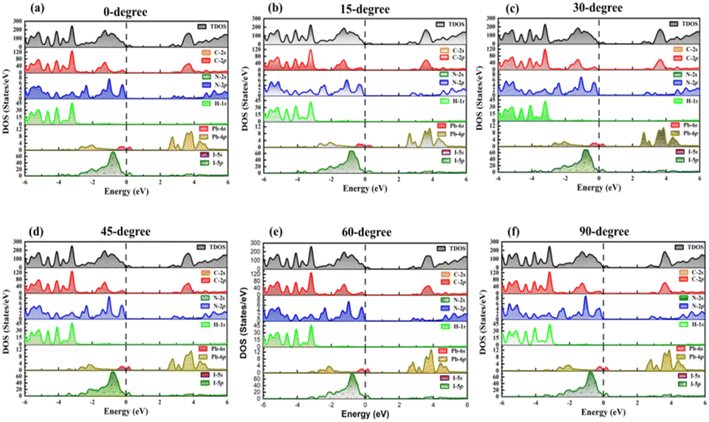 | ||
| Fig. 3 PDOS for (a) 0-degree, (b) 15-degree, (c) 30-degree, (d) 45-degree, (e) 60-degree, (f) 90-degree orientation of TPBi. | ||
Our findings confirm that changes in TPBi orientation trigger pronounced charge redistribution due to charge hybridization at the interface. This interaction results in the emergence of interfacial states, leaving a distinct mark on the TDOS profiles of TPBi–(PEA)2PbI4 heterostructures, differentiating them from the TDOS of (PEA)2PbI4. In our study of TPBi–(PEA)2PbI4 heterostructures, we examined the variations in HOMO and LUMO energy levels across different orientations. Detailed bandgap values for all TPBi–(PEA)2PbI4 heterostructures are compiled in Table S2.† Remarkably, despite significant disparities in HOMO and LUMO values as well as the bandgap, both the 15-degree and 60-degree orientations yield approximately similar charge transfer values. The 15-degree orientation registers the highest charge transfer value of 0.403 e, while the 60-degree orientation records a charge transfer value of 0.401 e. This intriguing observation suggests that the strategic choice of TPBi orientation may effectively alleviate disparities in charge transport characteristics. Notably, TPBi orientation emerges as a pivotal factor influencing this intricate process. The observed equilibrium in charge transport efficiency across diverse orientations strongly implies the substantial involvement of additional factors, including carrier mobility, interfacial states, and energy barriers, in shaping these dynamic phenomena.
Expanding upon our analysis of the TDOS, the PDOS analysis allows us to delve deeper into the intricate contributions of individual orbitals to the formation of the valence and conduction bands in TPBi–(PEA)2PbI4 and (PEA)2PbI4, while considering their HOMO and LUMO levels. Fig. 3(a–f) presents the PDOS profiles of selected TPBi orientations for TPBi–(PEA)2PbI4 heterostructures, offering a view of the specific orbital contributions. At the same time, Fig. S3† focuses on (PEA)2PbI4, giving insight into the role of pseudo-electrons associated with each constituent element in shaping these bands. What's particularly interesting is the composition of the valence band, where the dominant contributions in TPBi–(PEA)2PbI4 heterostructures come from the 2p-orbitals of Carbon (C) and Nitrogen (N) atoms. Following closely are the 5p-orbitals of Iodine (I) atoms, which also contribute substantially to the valence band formation. These contributions play a significant role in defining the electronic structure of the valence band. The energy levels of these contributions are associated with the HOMO levels of the material. In a sharp departure, Fig. S3† presents a distinct scenario within (PEA)2PbI4, where the primary influence on shaping the valence band is attributed to the 5p-orbitals of I atoms and 6s-orbitals of Lead (Pb) atoms situated in proximity to the Fermi level. These I and Pb orbitals exert a substantial impact on the HOMO level of (PEA)2PbI4 and play a crucial role in defining its electronic characteristics. Moreover, a subtle hybridization exists with the 2p-orbitals of C atoms at an energy level near −2 eV. The lower energy levels within the valence band of (PEA)2PbI4 are markedly influenced by the hybridization of diverse orbitals. This encompasses the blending of 2p-orbitals from C atoms and 2p-orbitals originating from N atoms, in conjunction with the 1s-orbitals associated with hydrogen (H) atoms. These orbital interactions give rise to the formation of electronic states situated within the lower energy range of the valence band, thus contributing to the overall electronic structure of (PEA)2PbI4, including the determination of its HOMO level. Conversely, the LUMO level correlates with the energy levels residing in the conduction band. The evaluation of the electronic structure and the contributions from distinct orbitals to the conduction band in both TPBi–(PEA)2PbI4 and (PEA)2PbI4 would conform to a comparable analytical framework, thereby shedding light on the LUMO levels of these materials.
Shifting our focus to the formation of the conduction band reveals the pivotal roles specific orbitals play in shaping electronic states across varying energy levels. Notably, the 6s-orbitals of Pb atoms take centre stage in defining states at lower energy levels within the conduction band. These Pb 6s-orbitals exhibit robust hybridization with the 2p-orbitals of C atoms, giving rise to electronic states that significantly influence the lower energy range of the conduction band. In contrast, the 2p-orbitals of C and N atoms and the 5p-orbitals of I atoms make comparatively modest contributions to the higher energy range of the conduction band. A crucial observation arises when comparing the PDOS profiles of TPBi–(PEA)2PbI4 heterostructures in Fig. 3(a–f) with the DOS of (PEA)2PbI4 featured in Fig. S3.† Notably, the prominent peaks on the valence band side in TPBi–(PEA)2PbI4 heterostructures can be primarily attributed to the 5p-orbitals of I atoms within (PEA)2PbI4, particularly in the vicinity of the Fermi level. Furthermore, there is a modest contribution from the hybridized states of 2p-orbitals of C and N atoms from TPBi. It is evident that TPBi strongly influences the DOS, which is clearly highlighted by comparing the results of TPBi–(PEA)2PbI4 heterostructures shown in Fig. S2(a–f).† Similarly, the significant peaks near the Fermi level on the conduction band side of TPBi–(PEA)2PbI4 heterostructures are primarily due to the 6p orbitals of Pb atoms within (PEA)2PbI4. These 6p orbitals are complemented by the hybridization of 2p-orbitals of C and N atoms from both (PEA)2PbI4 and TPBi. Collectively, these detailed PDOS profiles reveal the profound impact of TPBi orientation on interfacial hybridizations within TPBi–(PEA)2PbI4 heterostructures. This, in turn, significantly influences the DOS and leads to noteworthy alterations in electronic properties and charge transfer behaviour within the TPBi–(PEA)2PbI4 heterostructure.
To delve deeper into the charge transfer characteristics of heterostructures, we've depicted the isosurface charge density difference using Bader charge analysis in Fig. 4. This figure illustrates the distribution of charges within the Bader volume associated with specific atoms, thereby revealing the total charge carried by each atom. A positive Bader value indicates a decrease in charge carriers, whereas a negative value indicates an increase in charge carriers. In our prior investigation centred on TPBi–FAPbI3 heterostructures,58 our Bader charge analysis consistently revealed a distinct charge depletion pattern at C and Pb atoms, indicative of their cationic nature. Meanwhile, N, I, and H atoms consistently demonstrated charge accumulation. It's noteworthy that in our previous research, TPBi–FAPbI3 highlighted a significant finding – an average charge transfer of 0.570 e for the 15-degree orientation, confirming excellent efficiency in electron transport at the interface. Our recent study focusing on TPBi–(PEA)2PbI4 heterostructures showed a distinctive charge depletion at both C and Pb atoms, indicating their cationic nature. Conversely, there is a consistent accumulation of charge at N and H atoms. An intriguing observation arises as we identified anomalous behaviours of I atoms through Bader charge analysis. Upon careful examination (Fig. 4), we observed that the corresponding charge transfer value is lower when the I atom carries a more negative or a less positive charge in specific orientations. Conversely, the charge transfer is higher in orientations where the positive charge is higher, or the negative charge is lower. Notably, in the case of a 60-degree orientation, the H atoms exhibited a substantial positive charge. This observation elucidates why the charge transfer for the 60-degree orientation is roughly equivalent to that of the 15-degree orientation. Remarkably, this observation consistently aligns with our findings from PDOS results, underscoring the significant contribution of I atoms to the formation of the valence band. Our latest research emphasizes the enduring importance of TPBi orientations in enhancing charge transfer within TPBi–(PEA)2PbI4 interfaces, providing insightful distinctions in charge transfer properties compared to TPBi–FAPbI3 heterostructures.
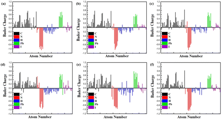 | ||
| Fig. 4 Bader Charge analysis of TPBi molecule at (a) 0-degree, (b) 15-degree, (c) 30-degree, (d) 45-degree, (e) 60-degree, and (f) 90-degree orientation at the surface of (PEA)2PbI4. | ||
Isosurface analysis offers a detailed examination of charge density distributions and their variations within a given volume. This technique involves the generation of three-dimensional surfaces that represent regions of constant charge density, providing a visual representation of electron distribution and indicating the charge transfer phenomena occurring within complex heterostructures. In this study, we utilize isosurface analysis to explore the charge transfer characteristics of heterostructures, unravelling subtle nuances in charge dynamics and enhancing our understanding of the material's electronic behaviour. Fig. 5(a–f) visually represents these assessments for various TPBi orientations (0-degree, 15-degree, 30-degree, 45-degree, 60-degree and 90-degree). To visualize these distinctive features, we harnessed the capabilities of the Vesta software package.68 An isosurface value of 0.0002 was thoughtfully selected, complemented by a section opacity set at 0% to provide a crystal-clear view. In this visual representation, the red regions clearly outline areas of charge accumulation, while the green regions showcased in Fig. 5 serve as a compelling visual testament to the depletion of charge carriers. These graphical depictions underscore that the interface experiences the lowest charge transfer when TPBi is oriented at 90-degree. In stark contrast, the most rapid charge transfer is observed when TPBi is inclined at a 15-degree and 60-degree angle concerning (PEA)2PbI4. The charge transfer rate shows a progressive increase with shifts in TPBi orientation, following the sequence of 90-degree, 0-degree, 45-degree, 30-degree, 60-degree, and 15-degree. This variation in the rate of vdW interactions for different orientations of the TPBi–(PEA)2PbI4 heterostructure implies heightened atomic layer interactions within the heterostructure, which could plausibly elucidate the observed differences in charge transfer dynamics.
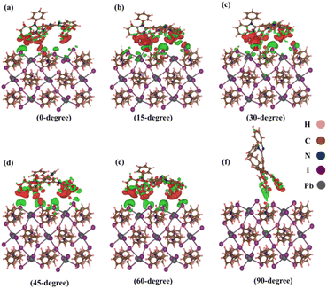 | ||
| Fig. 5 Isosurface charge density at (0 1 0) surface of (PEA)2PbI4 with (a) 0-degree, (b) 15-degree, (c) 30-degree, (d) 45-degree, (e) 60-degree, (f) 90-degree orientation of TPBi. | ||
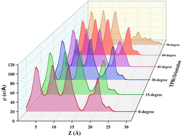
To comprehensively understand the surface characteristics of the TPBi layer and the underlying mechanisms governing charge transport at the interfaces, we present visual representations in Fig. 6 and 7, showcasing the averaged charge density and integrated charge density difference along the z-axis respectively. For a detailed examination of the individual heterostructures, please refer to Fig. S4 and S5,† which provide the averaged charge density and integrated charge density difference along the z-axis for each of the six orientations (0-degree, 15-degree, 30-degree, 45-degree, 60-degree, and 90-degree). Our average charge density data encompasses both positive and negative values, shedding light on the spatial distribution of electrons at specific z (Å) positions. Notably, we observe prominent peaks within the z-range of 0 Å to 16 Å, indicating a significant electron density within the initial three atomic layers of (PEA)2PbI4, a characteristic feature of perovskite materials. However, as we extend the analysis beyond the 16 Å z-value, the final peak exhibits a relatively lower intensity, corresponding to the TPBi layer. A compelling point of contrast arises when comparing these findings to our prior research on FAPbI3, where we considered a broader z-range (0 Å to 27 Å). This significant variation accentuates the material-specific disparities in electron distribution at the interfaces. To bridge these analyses, we explore the comparison with TPBi–FAPbI3 interfaces, shedding light on material-specific disparities in electron distribution at the interfaces.
Compared to the TPBi–FAPbI3 interfaces, a sharp decline in charge density in the TPBi–(PEA)2PbI4 interfaces suggests a limited number of electrons, attributed to intricate electronic charge hybridization. As shown in Fig. S6,† in the TPBi–(PEA)2PbI4 heterostructure, the surface of (PEA)2PbI4 displays only I atoms, and their proximity to TPBi is greater than that to Pb atoms. In contrast, in the TPBi–FAPbI3 heterostructure, both I and Pb atoms are present on the surface of FAPbI3, fostering easier interaction with TPBi. This difference in the proximity of Pb and I atoms influences the ease of interaction with TPBi. Upon comparing the 15-degree orientation for both heterostructures, it is evident that in the TPBi–FAPbI3 case, the charge transfer value is higher than the TPBi–(PEA)2PbI4 heterostructure. This discrepancy can be attributed to the presence of both I and Pb atoms on the surface of FAPbI3, facilitating a more efficient charge transfer interaction with TPBi. Interestingly, in the TPBi–(PEA)2PbI4 heterostructure, an approximately equal charge transfer is observed for 15-degree- and 60-degree orientations. Notably, these nearly identical charge transfer values suggest a unique behaviour, underscoring the collective influence of I and Pb atoms in facilitating charge transfer. This observation suggests a unique behaviour, indicating that I and Pb atoms collectively play a crucial role in charge transfer in this heterostructure. This is supported by the significant contribution of 5p-orbitals of I atoms to valence band formation and 6p-orbitals of Pb atoms to the conduction band. The distinctive charge transfer behaviour in TPBi–(PEA)2PbI4 highlights the nuanced interplay of atomic interactions, providing valuable insights into the material's electronic structure and charge transfer dynamics. These pronounced distinctions in charge transfer behaviour between TPBi–(PEA)2PbI4 and TPBi–FAPbI3 shed light on the intricate interplay of atomic interactions. These insights contribute to a deeper understanding of the electronic properties and transport dynamics at the interfaces, offering valuable knowledge for the development of advanced material systems.
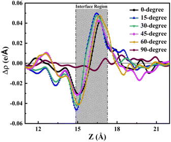
Likewise, the integrated charge density difference curve along the z-axis provides a quantitative perspective on charge transfer along this axis. As illustrated in Fig. 7, this curve reveals the charge transfer dynamics at the TPBi–(PEA)2PbI4 interface, offering insights into the charge accumulation and depletion between both layers. The interface region, delineated in Fig. 7, further highlights the nuanced variations in charge distribution. The interface region in Fig. 7 provides an estimation for all orientations, encapsulating the comprehensive charge transfer phenomena at the TPBi–(PEA)2PbI4 interface. The observed behaviour in Fig. 7 strikingly aligns with the patterns of accumulation and depletion identified in the Bader charge analysis, as depicted in Fig. 4. Specifically, I atoms at the surface of (PEA)2PbI4 are seen to deplete charges, while accumulation occurs at the nearby C atoms of TPBi. Furthermore, N atoms in TPBi also exhibit a significant accumulation of electrons. For a more detailed examination of the individual heterostructures, please refer to Fig. S5.† In Fig. S5,† the interface region for each structure is individually showcased, revealing a finer granularity of the charge transfer dynamics. Each structure's interface region is further divided into two distinct parts: accumulation and depletion. The accumulation regions are vividly marked in red, indicating areas where charge carriers gather, while the depletion regions are distinctly marked in green, representing zones where charge carriers are diminished. This detailed breakdown in Fig. S5† offers a comprehensive view of how each orientation contributes to the overall charge transfer dynamics. The intensity of the peaks, signifying accumulation and depletion, reinforces the earlier predictions regarding the 15-degree and 60-degree structures having the highest charge transfer efficiency, as previously suggested in the Bader charge analysis sections. These findings provide a comprehensive understanding of the charge transfer dynamics occurring at the TPBi–(PEA)2PbI4 interface, supporting the idea that specific TPBi orientations play a pivotal role in governing these interactions.
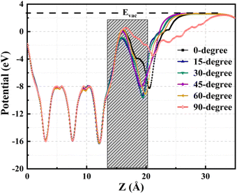
The averaged electrostatic potential along the z-axis is a valuable tool for elucidating crucial aspects of charge transfer characteristics, discerning the presence of electrons and holes at specific z-values. This potential provides a comprehensive profile of the electric charge distribution at different positions along the z-axis. The charge transfer process is intrinsically linked to the potential difference; electrons exhibit migration from regions characterized by low potential to those with higher potential, whereas holes traverse from areas of high potential to lower potential. Fig. 8 delineates electrostatic potential profiles for TPBi orientations on the (PEA)2PbI4 surface, with an estimated interface region and vacuum energy (Evac) level depicted for all orientations. Concurrently, Fig. S7† elucidates the respective electrostatic potential profiles corresponding to each TPBi orientation on the (PEA)2PbI4 surface, providing a detailed breakdown for each individual orientation, including the estimated interface region and Evac level. The data presented in the figures constitute a pivotal facet of the inquiry into the intermolecular forces and electronic interactions dictating the TPBi–(PEA)2PbI4 interface, furnishing valuable insights for a broader comprehension of the scrutinized system.
Significantly, the electrostatic potential profiles exhibit prominent negative peaks, signalling the substantial presence of electrons within (PEA)2PbI4. This observation is consistent with the findings from the averaged charge density plot, as illustrated in Fig. 6. A discernible rise in the electrostatic potential becomes apparent upon entering the region where TPBi is situated within each heterostructure. This noticeable increase implies a highly favourable propensity for electron transfer from (PEA)2PbI4 to TPBi within these regions. Furthermore, positive potential values substantiate the depletion of charges from TPBi to (PEA)2PbI4, aligning seamlessly with the insights outlined in the description of the isosurface charge density analysis. Therefore, these electrostatic potential profiles offer crucial insights into the dynamics of charge transfer between (PEA)2PbI4 and TPBi across the various orientations considered in our study.
Conclusions
Our study underscores the significant impact of molecular orientation on the efficiency, stability, and performance of perovskite devices, particularly evident at TPBi–(PEA)2PbI4 interfaces as determined through computational methods. Key findings include the effect of TPBi orientation at 15 and 60 degrees on charge transfer dynamics, where optimal orientations enhance device efficiency. Binding energy calculations offer insights into device stability, with the most stable structures at the 15 and 30-degree TPBi orientations. These findings are further substantiated by Bader charge, charge density, and isosurface analysis, which collectively confirm effective charge transfer mechanisms. This study highlights the role of interfacial molecular orientation in optimizing perovskite device performance and contributes to the development of low-dimensional optoelectronic devices, tapping into the full potential of perovskite materials for efficient and sustainable optoelectronics.Author contributions
S. Chang and Y. Zhu conceived and directed the project; S. M. K. A. Naqvi, H. Long, Z. Nazir and Y. Zhu prepared the models, carried out the simulations and prepared the figures; S. M. K. A. Naqvi, R. B. Vasiliev, O. Kulakovich and S. Chang analysed the data, interpreted the results and wrote the manuscript.Conflicts of interest
The authors declare no conflicts of interest.Acknowledgements
This work is supported by the National Natural Science Foundation of China (22211530439,22173009) and the 2022 Shenzhen Fundamental Research Program (20220818150511001). Y. Zhu acknowledges the financial support from the Foundation for Youth Innovative Talents in Higher Education of Guangdong Province (No. 2023KQNCX094) and the opening project of State Key Laboratory of Explosion Science and Technology (Beijing Institute of Technology) with the opening project number is KFJJ23-21M.References
- M. R. Filip, G. E. Eperon, H. J. Snaith and F. Giustino, Steric Engineering of Metal-Halide Perovskites with Tunable Optical Band Gaps, Nat. Commun., 2014, 5(1), 5757 CrossRef CAS PubMed.
- J. H. Noh, S. H. Im, J. H. Heo, T. N. Mandal and S. Seok, Il. Chemical Management for Colorful, Efficient, and Stable Inorganic–Organic Hybrid Nanostructured Solar Cells, Nano Lett., 2013, 13(4), 1764–1769 CrossRef CAS PubMed.
- G. Xing, N. Mathews, S. Sun, S. S. Lim, Y. M. Lam, M. Grätzel, S. Mhaisalkar and T. C. Sum, Long-Range Balanced Electron- and Hole-Transport Lengths in Organic–Inorganic CH3NH3PbI3, Science, 2013, 342(6156), 344–347 CrossRef CAS PubMed.
- S. D. Stranks, G. E. Eperon, G. Grancini, C. Menelaou, M. J. P. Alcocer, T. Leijtens, L. M. Herz, A. Petrozza and H. J. Snaith, Electron–Hole Diffusion Lengths Exceeding 1 Micrometer in an Organometal Trihalide Perovskite Absorber, Science, 2013, 342(6156), 341–344 CrossRef CAS PubMed.
- C. Wehrenfennig, G. E. Eperon, M. B. Johnston, H. J. Snaith and L. M. Herz, High Charge Carrier Mobilities and Lifetimes in Organolead Trihalide Perovskites, Adv. Mater., 2014, 26(10), 1584–1589 CrossRef CAS PubMed.
- M. A. Green, A. Ho-Baillie and H. J. Snaith, The Emergence of Perovskite Solar Cells, Nat. Photonics, 2014, 8(7), 506–514 CrossRef CAS.
- B. Liu, L.-J. Wu, Y.-Q. Zhao, L.-Z. Wang and M.-Q. Cai, Tuning the Schottky Barrier Height of the Pd–MoS2 Contact by Different Strains, Phys. Chem. Chem. Phys., 2015, 17(40), 27088–27093 RSC.
- B. Liu, L.-J. Wu, Y.-Q. Zhao, L.-Z. Wang and M.-Q. Cai, A First-Principles Study of Magnetic Variation via Doping Vacancy in Monolayer VS2, J. Magn. Magn. Mater., 2016, 420, 218–224 CrossRef CAS.
- L. Li, Y. Yu, G. J. Ye, Q. Ge, X. Ou, H. Wu, D. Feng, X. H. Chen and Y. Zhang, Black Phosphorus Field-Effect Transistors, Nat. Nanotechnol., 2014, 9(5), 372–377 CrossRef CAS PubMed.
- A. A. Balandin, S. Ghosh, W. Bao, I. Calizo, D. Teweldebrhan, F. Miao and C. N. Lau, Superior Thermal Conductivity of Single-Layer Graphene, Nano Lett., 2008, 8(3), 902–907 CrossRef CAS PubMed.
- D. Wang, B. Wen, Y.-N. Zhu, C.-J. Tong, Z.-K. Tang and L.-M. Liu, First-Principles Study of Novel Two-Dimensional (C4H9NH3)2PbX4 Perovskites for Solar Cell Absorbers, J. Phys. Chem. Lett., 2017, 8(4), 876–883 CrossRef CAS PubMed.
- L. Ma, J. Dai and X. C. Zeng, Two-Dimensional Single-Layer Organic–Inorganic Hybrid Perovskite Semiconductors, Adv. Energy Mater., 2017, 7(7), 1601731 CrossRef.
- M. Ju, J. Dai, L. Ma and X. C. Zeng, Perovskite Chalcogenides with Optimal Bandgap and Desired Optical Absorption for Photovoltaic Devices, Adv. Energy Mater., 2017, 7(18), 1700216 CrossRef.
- Z. Xiao, W. Meng, J. Wang, D. B. Mitzi and Y. Yan, Searching for Promising New Perovskite-Based Photovoltaic Absorbers: The Importance of Electronic Dimensionality, Mater. Horiz., 2017, 4(2), 206–216 RSC.
- Z. Xiao and Y. Yan, Progress in Theoretical Study of Metal Halide Perovskite Solar Cell Materials, Adv. Energy Mater., 2017, 7(22), 1701136 CrossRef.
- L. Zhang and W. Liang, How the Structures and Properties of Two-Dimensional Layered Perovskites MAPbI3 and CsPbI3 Vary with the Number of Layers, J. Phys. Chem. Lett., 2017, 8(7), 1517–1523 CrossRef CAS PubMed.
- L. Dou, A. B. Wong, Y. Yu, M. Lai, N. Kornienko, S. W. Eaton, A. Fu, C. G. Bischak, J. Ma and T. Ding, et al., Atomically Thin Two-Dimensional Organic–Inorganic Hybrid Perovskites, Science, 2015, 349(6255), 1518–1521 CrossRef CAS PubMed.
- Z. Tan, Y. Wu, H. Hong, J. Yin, J. Zhang, L. Lin, M. Wang, X. Sun, L. Sun and Y. Huang, et al., Two-Dimensional (C4H9NH3)2PbBr4 Perovskite Crystals for High-Performance Photodetector, J. Am. Chem. Soc., 2016, 138(51), 16612–16615 CrossRef CAS PubMed.
- J. Zhou, Y. Chu and J. Huang, Photodetectors Based on Two-Dimensional Layer-Structured Hybrid Lead Iodide Perovskite Semiconductors, ACS Appl. Mater. Interfaces, 2016, 8(39), 25660–25666 CrossRef CAS PubMed.
- S. Chen and G. Shi, Two-Dimensional Materials for Halide Perovskite-Based Optoelectronic Devices, Adv. Mater., 2017, 29(24), 1605448 CrossRef PubMed.
- Z. Cheng and J. Lin, Layered Organic–Inorganic Hybrid Perovskites: Structure, Optical Properties, Film Preparation, Patterning and Templating Engineering, CrystEngComm, 2010, 12(10), 2646 RSC.
- D. B. Mitzi, C. A. Feild, W. T. A. Harrison and A. M. Guloy, Conducting Tin Halides with a Layered Organic-Based Perovskite Structure, Nature, 1994, 369(6480), 467–469 CrossRef CAS.
- C. C. Stoumpos, D. H. Cao, D. J. Clark, J. Young, J. M. Rondinelli, J. I. Jang, J. T. Hupp and M. G. Kanatzidis, Ruddlesden–Popper Hybrid Lead Iodide Perovskite 2D Homologous Semiconductors, Chem. Mater., 2016, 28(8), 2852–2867 CrossRef CAS.
- A. Simbula, L. Wu, F. Pitzalis, R. Pau, S. Lai, F. Liu, S. Matta, D. Marongiu, F. Quochi and M. Saba, et al., Exciton Dissociation in 2D Layered Metal-Halide Perovskites, Nat. Commun., 2023, 14(1), 4125 CrossRef CAS PubMed.
- X. Gao, X. Zhang, W. Yin, H. Wang, Y. Hu, Q. Zhang, Z. Shi, V. L. Colvin, W. W. Yu and Y. Zhang, Ruddlesden–Popper Perovskites: Synthesis and Optical Properties for Optoelectronic Applications, Adv. Sci., 2019, 6(22), 1900941 CrossRef CAS PubMed.
- Y. Lei, Y. Li, C. Lu, Q. Yan, Y. Wu, F. Babbe, H. Gong, S. Zhang, J. Zhou and R. Wang, et al., Perovskite Superlattices with Efficient Carrier Dynamics, Nature, 2022, 608(7922), 317–323 CrossRef CAS PubMed.
- J. You, L. Meng, T.-B. Song, T.-F. Guo, Y. M. Yang, W.-H. Chang, Z. Hong, H. Chen, H. Zhou and Q. Chen, et al., Improved Air Stability of Perovskite Solar Cells via Solution-Processed Metal Oxide Transport Layers, Nat. Nanotechnol., 2016, 11(1), 75–81 CrossRef CAS PubMed.
- K. Du, Q. Tu, X. Zhang, Q. Han, J. Liu, S. Zauscher and D. B. Mitzi, Two-Dimensional Lead(II) Halide-Based Hybrid Perovskites Templated by Acene Alkylamines: Crystal Structures, Optical Properties, and Piezoelectricity, Inorg. Chem., 2017, 56(15), 9291–9302 CrossRef CAS PubMed.
- B. Saparov and D. B. Mitzi, Organic–Inorganic Perovskites: Structural Versatility for Functional Materials Design, Chem. Rev., 2016, 116(7), 4558–4596 CrossRef CAS PubMed.
- D. B. Straus, N. Iotov, M. R. Gau, Q. Zhao, P. J. Carroll and C. R. Kagan, Longer Cations Increase Energetic Disorder in Excitonic 2D Hybrid Perovskites, J. Phys. Chem. Lett., 2019, 10(6), 1198–1205 CrossRef CAS PubMed.
- W. Peng, J. Yin, K.-T. Ho, O. Ouellette, M. De Bastiani, B. Murali, O. El Tall, C. Shen, X. Miao and J. Pan, et al., Ultralow Self-Doping in Two-Dimensional Hybrid Perovskite Single Crystals, Nano Lett., 2017, 17(8), 4759–4767 CrossRef CAS PubMed.
- B. Cheng, T.-Y. Y. Li, P.-C. C. Wei, J. Yin, K.-T. T. Ho, J. R. D. Retamal, O. F. Mohammed and J.-H. H. He, Layer-Edge Device of Two-Dimensional Hybrid Perovskites, Nat. Commun., 2018, 9(1), 5196 CrossRef PubMed.
- W. Niu, A. Eiden, G. Vijaya Prakash and J. J. Baumberg, Exfoliation of Self-Assembled 2D Organic–Inorganic Perovskite Semiconductors, Appl. Phys. Lett., 2014, 104(17), 171111 CrossRef.
- B. Liu, M. Long, M.-Q. Cai and J. Yang, Two-Dimensional van Der Waals Heterostructures Constructed via Perovskite (C4H9NH3)2XBr4 and Black Phosphorus, J. Phys. Chem. Lett., 2018, 9(17), 4822–4827 CrossRef CAS PubMed.
- H. Tsai, W. Nie, J.-C. Blancon, C. C. Stoumpos, R. Asadpour, B. Harutyunyan, A. J. Neukirch, R. Verduzco, J. J. Crochet and S. Tretiak, et al., High-Efficiency Two-Dimensional Ruddlesden–Popper Perovskite Solar Cells, Nature, 2016, 536(7616), 312–316 CrossRef CAS PubMed.
- Y. Sanehira, Y. Numata, M. Ikegami and T. Miyasaka, Photovoltaic Properties of Two-Dimensional (CH3(CH2)3NH3)2PbI4 Perovskite Crystals Oriented with TiO2 Nanowire Array, Chem. Lett., 2017, 46(8), 1204–1206 CrossRef CAS.
- C. Li, K. P. Loh and K. Leng, Organic–Inorganic Hybrid Perovskites and Their Heterostructures, Matter, 2022, 5(12), 4153–4169 CrossRef CAS.
- J. Zhang, X. Zhu, M. Wang and B. Hu, Establishing Charge-Transfer Excitons in 2D Perovskite Heterostructures, Nat. Commun., 2020, 11(1), 2618 CrossRef CAS PubMed.
- J. N. Coleman, M. Lotya, A. O'Neill, S. D. Bergin, P. J. King, U. Khan, K. Young, A. Gaucher, S. De and R. J. Smith, et al., Two-Dimensional Nanosheets Produced by Liquid Exfoliation of Layered Materials, Science, 2011, 331(6017), 568–571 CrossRef CAS PubMed.
- H. Liu, A. T. Neal, Z. Zhu, Z. Luo, X. Xu, D. Tománek and P. D. Ye, Phosphorene: An Unexplored 2D Semiconductor with a High Hole Mobility, ACS Nano, 2014, 8(4), 4033–4041 CrossRef CAS PubMed.
- H. D. C. N. Gunawardana, K. Osada, K. R. Koswattage and Y. Noguchi, Enhancement of the Molecular Orientation of TPBi in Coevaporated Films of UGH-2 Host Molecules, Surf. Interface Anal., 2021, 53(4), 460–465 CrossRef CAS.
- A. Senes, S. C. J. Meskers, W. M. Dijkstra, J. J. van Franeker, S. Altazin, J. S. Wilson and R. A. J. Janssen, Transition Dipole Moment Orientation in Films of Solution Processed Fluorescent Oligomers: Investigating the Influence of Molecular Anisotropy, J. Mater. Chem. C, 2016, 4(26), 6302–6308 RSC.
- J. Calimano, F. Li, J. Florián, D. M. Piñero-Cruz, T. R. Fielitz, R. J. Holmes and J. W. Ciszek, Solid-State Properties and Spectroscopic Analysis of Thin-Film TPBi, J. Phys. Chem. C, 2020, 124(43), 23716–23723 CrossRef CAS.
- Y. Watanabe, H. Sasabe and J. Kido, Review of Molecular Engineering for Horizontal Molecular Orientation in Organic Light-Emitting Devices, Bull. Chem. Soc. Jpn., 2019, 92(3), 716–728 CrossRef CAS.
- D. Cui, S. Wang, S. Li, Y. Liu, X. Gao, W. Wang and X. Dong, Improving the Performance of OLEDs by Controlling the Molecular Orientation in Charge Carrier Transport Layers, Opt. Express, 2021, 29(11), 16845 CrossRef CAS PubMed.
- T. D. Schmidt, T. Lampe, D. Sylvinson M. R., P. I. Djurovich, M. E. Thompson and W. Brütting, Emitter Orientation as a Key Parameter in Organic Light-Emitting Diodes, Phys. Rev. Appl., 2017, 8(3), 037001 CrossRef.
- R. A. Marcus, On the Theory of Oxidation-Reduction Reactions Involving Electron Transfer. I, J. Chem. Phys., 1956, 24(5), 966–978 CrossRef CAS.
- H. Bässler, Charge Transport in Disordered Organic Photoconductors a Monte Carlo Simulation Study, Phys. Status Solidi, 1993, 175(1), 15–56 CrossRef.
- S. Grimme, Density Functional Theory with London Dispersion Corrections, Wiley Interdiscip. Rev.: Comput. Mol. Sci., 2011, 1(2), 211–228 CAS.
- F. London, The General Theory of Molecular Forces, Trans. Faraday Soc., 1937, 33, 8b–26 RSC.
- W. S. Yang, J. H. Noh, N. J. Jeon, Y. C. Kim, S. Ryu, J. Seo and I. S. Seok, High-Performance Photovoltaic Perovskite Layers Fabricated through Intramolecular Exchange, Science, 2015, 348(6240), 1234–1237 CrossRef CAS PubMed.
- Q. Wang, Y. Shao, Q. Dong, Z. Xiao, Y. Yuan and J. Huang, Large Fill-Factor Bilayer Iodine Perovskite Solar Cells Fabricated by a Low-Temperature Solution-Process, Energy Environ. Sci., 2014, 7(7), 2359–2365 RSC.
- M. Liu, M. B. Johnston and H. J. Snaith, Efficient Planar Heterojunction Perovskite Solar Cells by Vapour Deposition, Nature, 2013, 501(7467), 395–398 CrossRef CAS PubMed.
- S. Luo and W. A. Daoud, Recent Progress in Organic–Inorganic Halide Perovskite Solar Cells: Mechanisms and Material Design, J. Mater. Chem. A, 2015, 3(17), 8992–9010 RSC.
- M. M. Lee, J. Teuscher, T. Miyasaka, T. N. Murakami and H. J. Snaith, Efficient Hybrid Solar Cells Based on Meso-Superstructured Organometal Halide Perovskites, Science, 2012, 338(6107), 643–647 CrossRef CAS PubMed.
- D. Ji, L. Li, H. Fuchs and W. Hu, Engineering the Interfacial Materials of Organic Field-Effect Transistors for Efficient Charge Transport, Acc. Mater. Res., 2021, 2(3), 159–169 CrossRef CAS.
- Z. Hu, F. Huang and Y. Cao, Layer-by-Layer Assembly of Multilayer Thin Films for Organic Optoelectronic Devices, Small Methods, 2017, 1(12), 1700264 CrossRef.
- S. M. K. A. Naqvi, Y. Zhu and S. Chang, Manipulating Interfacial Performance of TPBi–FAPbI3 Perovskite Interfaces Based on TPBi Orientations: A Theoretical Perspective, J. Phys. Chem. C, 2023, 127(46), 22752–22759 CrossRef CAS.
- Y. Huang, T. Liu, B. Wang, J. Li, D. Li, G. Wang, Q. Lian, A. Amini, S. Chen and C. Cheng, et al., Antisolvent Engineering to Optimize Grain Crystallinity and Hole-Blocking Capability of Perovskite Films for High-Performance Photovoltaics, Adv. Mater., 2021, 33(38), 2102816 CrossRef CAS PubMed.
- G. Kresse and J. Furthmüller, Efficiency of Ab Initio Total Energy Calculations for Metals and Semiconductors Using a Plane-Wave Basis Set, Comput. Mater. Sci., 1996, 6(1), 15–50 CrossRef CAS.
- M. D. Hanwell, D. E. Curtis, D. C. Lonie, T. Vandermeersch, E. Zurek and G. R. A. Hutchison, An Advanced Semantic Chemical Editor, Visualization, and Analysis Platform, J. Cheminf., 2012, 4(1), 17 CAS.
- M. Ernzerhof and G. E. Scuseria, Assessment of the Perdew–Burke–Ernzerhof Exchange-Correlation Functional, J. Chem. Phys., 1999, 110(11), 5029–5036 CrossRef CAS.
- J. P. Perdew, K. Burke and M. Ernzerhof, Generalized Gradient Approximation Made Simple, Phys. Rev. Lett., 1996, 77(18), 3865–3868 CrossRef CAS PubMed.
- M. Robert, Oxygen Affinity of Haemoglobin (Author's Transl), Bull. Physio-Pathol. Respir., 1975, 11(1), 79–170 CAS.
- C. Lee, W. Yang and R. G. Parr, Development of the Colle-Salvetti Correlation-Energy Formula into a Functional of the Electron Density, Phys. Rev. B: Condens. Matter Mater. Phys., 1988, 37(2), 785–789 CrossRef CAS PubMed.
- A. D. Becke, A New Mixing of Hartree–Fock and Local Density-Functional Theories, J. Chem. Phys., 1993, 98(2), 1372–1377 CrossRef CAS.
- V. A. Rassolov, M. A. Ratner, J. A. Pople, P. C. Redfern and L. A. Curtiss, 6-31G* Basis Set for Third-row Atoms, J. Comput. Chem., 2001, 22(9), 976–984 CrossRef CAS.
- K. Momma and F. Izumi, VESTA 3 for Three-Dimensional Visualization of Crystal, Volumetric and Morphology Data, J. Appl. Crystallogr., 2011, 44(6), 1272–1276 CrossRef CAS.
Footnote |
| † Electronic supplementary information (ESI) available: Computational methods details and heterostructure optimizations by VASP with all the processing data. See DOI: https://doi.org/10.1039/d4na00186a |
| This journal is © The Royal Society of Chemistry 2024 |

