 Open Access Article
Controlling the electronic and magnetic properties of the GeAs monolayer by generating Ge vacancies and doping with transition-metal atoms†
D. M.
Hoat
 *ab,
R.
Ponce-Pérez
c,
Chu Viet
Ha
d and
J.
Guerrero-Sanchez
c
aInstitute of Theoretical and Applied Research, Duy Tan University, Ha Noi 100000, Vietnam. E-mail: dominhhoat@duytan.edu.vn
bFaculty of Natural Sciences, Duy Tan University, Da Nang 550000, Vietnam
cUniversidad Nacional Autónoma de México, Centro de Nanociencias y Nanotecnología, Apartado Postal 14, Ensenada, Baja California Código Postal 22800, Mexico
dFaculty of Physics, TNU-University of Education, Thai Nguyen, 250000, Vietnam
First published on 21st May 2024
Abstract
Controlling the electronic and magnetic properties of two-dimensional (2D) materials is a key step to make new multifunctional candidates for practical applications. In this work, defects and doping with transition metals (TMs = V, Cr, Mn, and Fe) at Ge sublattices are proposed in order to develop novel features in the hexagonal germanium arsenide (GeAs) monolayer. The pristine GeAs monolayer is a non-magnetic indirect gap semiconductor with an energy gap of 1.20(1.82) eV as provided by PBE(HSE06)-based calculations. A single Ge vacancy metallizes the monolayer, preserving its non-magnetic nature. In contrast, significant magnetization with a total magnetic moment of 1.96 μB is achieved by a pair of Ge vacancies. Herein, the computed band structures assert the half-metallic behavior of the defective system. Similarly, half-metallicity is also obtained by V, Mn, and Fe doping. Meanwhile, the Cr-doped GeAs monolayer is classified as a diluted magnetic semiconductor 2D system. In these cases, magnetic properties are produced mainly by TM-3d electrons with total magnetic moments between 2.00 and 4.00 μB. Further, the effects of substituting a pair of Ge atoms with a pair of TM atoms (pTMGe systems) are also investigated. Results indicate the ferromagnetic half-metallicity of the pVGe system, meanwhile antiferromagnetic ordering is stable in the remaining cases. In all cases, TM impurities transfer charge to the host GeAs monolayer since they are surrounded by As atoms, which are more electronegative than dopant atoms. Results presented herein may introduce new 2D systems – made from the non-magnetic GeAs monolayer – for spintronic applications with suitable electronic and magnetic features controlled mainly by transition metals.
1. Introduction
Nano-scale systems have drawn enormous attention from the scientific community in order to develop new materials for rapid advances in technology.1–4 In this regard, the successful exfoliation of graphene has stimulated extensive investigations in the field of two-dimensional (2D) materials. In particular, graphene holds exclusive properties including high carrier mobility, high thermal conductivity, excellent mechanical strength, high surface/volume ratio, 97.2% transparency, and single molecule adsorption.5–7 At a rapid rate, the synthesis of 2D materials has taken place using different advanced methods such as mechanical and electrochemical exfoliation,8,9 chemical vapor deposition (CVD),10,11 and molecular beam epitaxy (MBE).12,13 Research efforts have been devoted to the discovery of a large variety of other 2D materials besides graphene derivatives.14,15 For example, hexagonal boron nitride (h-BN),16,17 transition metal dichalcogenides (TMDs),18,19 silicene,20 and phosphorene,21,22 among others, have been fabricated successfully. Besides, theoretical calculations have been widely utilized to predict the stability as well as ground state properties of new 2D compounds.23,24 Unique physical, chemical, and mechanical properties have made 2D materials potential candidates for a wide range of applications such as optoelectronics and electronics,25,26 energy storage,27,28 photodetection,29,30 gas sensing,31,32 catalysis,33,34 and spintronics.35,36Recently, along with other IV–V group 2D semiconductor materials, germanium arsenide (GeAs) has been considered by researchers. 2D GeAs has been grown by Barreteau et al.37 using the melt-growth method under high pressure. Characterization demonstrates its layered structure and semiconductor behavior. Guo et al.38 have fabricated p-type transistors based on few-layer GeAs with hole carrier mobility up to 99 cm2 V−1 s−1 and an ON–OFF ratio of 102. Moreover, a fast and intensive photoresponse is also observed in the mid-infrared regime. The promise of 2D GeAs crystals for polarization optical applications has been also demonstrated by Zhou et al.,39 where high dichroic ratios of Ipmax/Ipmin ∼ 1.49 and 4.4 at 520 and 830 nm are obtained, respectively. A field emission (FE) current from GeAs – with a turn-on field of ∼80 V μm−1 and current density higher than 10 A cm−2 – has been observed by Bartolomeo et al.,40 which suggests the suitability of this 2D material to be used as a cold cathode for electron emission. With an energy gap in the desirable range, 2D GeAs has also been recommended for photocatalytic applications towards water splitting.41
On the other hand, researchers have made efforts to develop new materials with desirable features for spintronic applications to meet the rapid advances of this field.42,43 Spin-based electronics demand highly spin-polarized materials with significant magnetic properties. Nevertheless, most of the discovered 2D materials have no intrinsic magnetism, and the 2D GeAs semiconductor is an example. In this work, our main aim is to propose efficient approaches to achieve proper magnetization of the GeAs monolayer in a hexagonal structure (belonging to the P![[6 with combining macron]](https://www.rsc.org/images/entities/char_0036_0304.gif) m2 space group) towards spintronic applications. Keeping in mind the effectiveness and simplicity of realizing vacancies and doping in 2D materials,44,45 structural modification at Ge sites is proposed. Specifically, a single Ge vacancy and a pair of Ge vacancies are investigated. Moreover, doping with a single TM atom and a pair of TM atoms (TM = transition metal: V, Cr, Mn, and Fe) is also considered. Our calculated doping energy indicates that the Ge site is preferable for transition metals to be doped in the GeAs monolayer (see Fig. S1 of the ESI file†). It is anticipated that significant magnetization of the GeAs monolayer is achieved, where feature-rich half-metallicity, and diluted magnetic semiconductor and antiferromagnetic semiconductor characteristics are obtained. Results suggested the defective and doped 2D GeAs systems as prospective 2D spintronic alternatives.
m2 space group) towards spintronic applications. Keeping in mind the effectiveness and simplicity of realizing vacancies and doping in 2D materials,44,45 structural modification at Ge sites is proposed. Specifically, a single Ge vacancy and a pair of Ge vacancies are investigated. Moreover, doping with a single TM atom and a pair of TM atoms (TM = transition metal: V, Cr, Mn, and Fe) is also considered. Our calculated doping energy indicates that the Ge site is preferable for transition metals to be doped in the GeAs monolayer (see Fig. S1 of the ESI file†). It is anticipated that significant magnetization of the GeAs monolayer is achieved, where feature-rich half-metallicity, and diluted magnetic semiconductor and antiferromagnetic semiconductor characteristics are obtained. Results suggested the defective and doped 2D GeAs systems as prospective 2D spintronic alternatives.
2. Computational details
Theoretical calculations are performed employing the Density Functional Theory (DFT) framework46 based on the Projector Augmented Wave method – as implemented in the advanced Vienna ab initio simulation package (VASP).47,48 The Generalized Gradient Approximation with the Perdew–Burke–Ernzerhof (PBE) version is adopted for description of the electron exchange-correlation potential.49 Considering the strong correlation effects of 3d electrons, the DFT + U method by Dudarev et al.50 is utilized with the on-site coulombic interaction parameters Ueff of 3.25, 3.70, 3.90, and 5.40 for V, Cr, Mn, and Fe atoms,51 respectively. The DFT-D3 method52 is introduced in calculations to consider the effects of the weak van der Waals interactions. An energy cutoff of 500 eV is chosen to realize the plane-wave expansion. The energy convergence is determined with a criterion of 10−6 eV. The structures are relaxed until the residual forces on individual atoms are less than 10−2 eV Å−1 A Γ-centered k-grid of 20 × 20 × 1 is generated using the Monkhorst–Pack method53 to sample the Brillouin zone of the primitive cell GeAs monolayer. To simulate the defects and doping, a 4 × 4 × 1 supercell containing 64 atoms is constructed. In these cases, a Monkhorst–Pack k-mesh of 4 × 4 × 1 is used. Furthermore, a vacuum gap wider than 14 Å is included in the direction perpendicular to the monolayer plane to avoid the inter-layer interactions.3. Results and discussion
3.1 Pristine GeAs monolayer
A unit cell of the GeAs monolayer is visualized in Fig. 1a, where one can see two vertically aligned Ge atoms inserted between two As atoms to form the As–Ge–Ge–As atomic stacking. From the top-view, the monolayer has a hexagonal structure with alternating Ge and As atoms, such that the structure is ascribed to the P![[6 with combining macron]](https://www.rsc.org/images/entities/char_0036_0304.gif) m2 space group (no. 187). From our calculations of structural relaxation, the following parameters are obtained for the GeAs monolayer unit cell: (1) lattice constant a = 3.82 Å; (2) chemical bond lengths dGe–As = 2.49 Å and dGe–Ge = 2.50 Å; (3) structural buckling height Δtotal = 2 × ΔAs–Ge + ΔGe–Ge = 2 × 1.15 + 2.50 = 4.80 Å; and (4) interatomic angles ∠AsGeAs = 100.36° and ∠AsGeGe = 117.54°. Once optimized, the stability of the GeAs monolayer was investigated using the following criteria:
m2 space group (no. 187). From our calculations of structural relaxation, the following parameters are obtained for the GeAs monolayer unit cell: (1) lattice constant a = 3.82 Å; (2) chemical bond lengths dGe–As = 2.49 Å and dGe–Ge = 2.50 Å; (3) structural buckling height Δtotal = 2 × ΔAs–Ge + ΔGe–Ge = 2 × 1.15 + 2.50 = 4.80 Å; and (4) interatomic angles ∠AsGeAs = 100.36° and ∠AsGeGe = 117.54°. Once optimized, the stability of the GeAs monolayer was investigated using the following criteria:
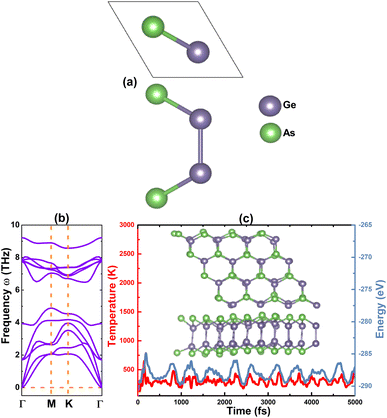 | ||
| Fig. 1 (a) Atomic structure unit cell, (b) phonon dispersion curves, and (c) AIMD simulations at 300 K ((Inset): atomic structure 4 × 4 × 1 supercell after simulations) of the GeAs monolayer. | ||
• Phonon calculations are carried using the PHONOPY code,54 for which the finite displacement method is adopted. Remembering that phonon frequency reflects the stiffness of material bonds, an imaginary frequency (corresponding to the negative second derivative of energy) asserts the dynamic instability of the material and vice verse. Phonon spectra of the GeAs monolayer are given in Fig. 1b. There are four atoms in a unit cell, thus, corresponding to two phonon branches (three acoustic and nine optical modes). Importantly, all phonon frequencies meet the condition of ω > 0 (with positive values) of material stability. These results indicate that the GeAs monolayer is dynamically stable.
• Ab initio molecular dynamic (AIMD) simulations are carried out at room temperature 300 K using the 4 × 4 × 1 supercell of the GeAs monolayer. Herein, a NVT ensemble and Nose–Hoover thermostat are utilized,55,56 and the time step is set to 5 fs with a total time of 5 ps. Results displayed in Fig. 1c show a slight movement of Ge and As atoms from their equilibrium sites, where no broken Ge–As and Ge–Ge bonds or geometric reconstruction (the initial hexagonal geometry is well-preserved) is observed. These results evidence that the GeAs monolayer is thermally stable.
• Elastic constants are calculated using the stress–strain method, where two constants C11 and C12 are required for the 2D hexagonal symmetry. According to Born's criteria, 2D materials hold good mechanical stability if C11 > 0 and C11 > |C12|.57 For the GeAs monolayer, our computations yield values of 81.95 and 30.65 N m−1 for C11 and C12 constants, respectively. Note that these values satisfy Born's criteria, suggesting that the GeAs monolayer is mechanically stable.
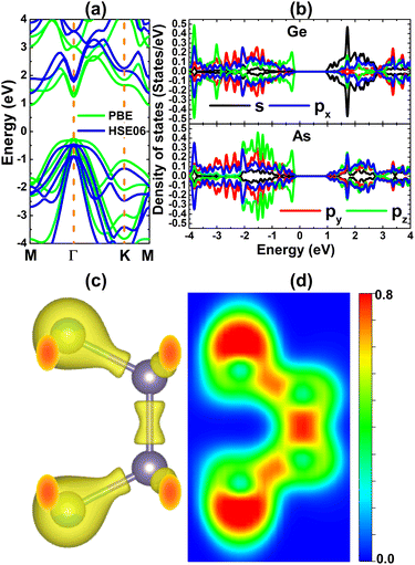
Once its stability is confirmed, the electronic properties of the GeAs monolayer are investigated. First, the electronic band structure is computed using PBE and the hybrid HSE06 functional.58 Theoretically, it can be expected that the HSE06 functional provides a more accurate calculation of the band gap of materials by including a 25% fraction of the exact Hartree exchange potential. Results plotted in Fig. 2a indicate that the GeAs monolayer is an indirect gap semiconductor, in which the valence band maximum and conduction band minimum are noted at the Γ and M points, respectively. Our PBE- and HSE06-based computations yield energy gaps of 1.20 and 1.82 eV, respectively. Note that these values are smaller than those of the monoclinic monolayer,41 indicating the important role of the structure in the GeAs monolayer energy gap. Then, the projected density of states (PDOS) of Ge and As atoms is calculated to analyze band structure formation. From PDOS spectra in Fig. 2b, a significant contribution from s and p orbitals of both constituent atoms is noted. Focusing on the regions close to the Fermi level, it can be seen that the upper part of the valence band is formed mainly by Ge-pz and As-pz states, while the Ge-s state generates mainly the lower part of the conduction band. To further investigate the chemical bonds, charge valence and electron localization in the GeAs monolayer are calculated, whose results are illustrated in Fig. 2c and d. Significant charge accumulations centered at As sites can be noted, indicating the ionic character of the Ge–As chemical bond. This feature is derived from the difference in the electronegativity of Ge and As atoms, which causes the charge transfer from the Ge (less electronegative) atom to the As (more electronegative) atom. This process is further confirmed by the Bader charge analysis, which indicates that a charge amount of 0.28 e is transferred from the Ge atom to the As atom. However, it will be flawed neglecting the covalent character, considering significant electronic hybridization of Ge-p and As-p orbitals (as observed in PDOS spectra). Therefore, the Ge–As chemical bond exhibits a mix of ionic and covalent characters. In addition, the Ge–Ge chemical bond is predominantly covalent because significant electrons are localized in the region between Ge atoms, which may be generated by sharing electrons.
3.2 Effects of Ge vacancies
In this part, the effects of a single Ge vacancy (VaGe system) and a pair of Ge vacancies (pVaGe system) on the electronic and magnetic properties of the GeAs monolayer are investigated. First, the formation energies Ef of VaGe and pVaGe systems are calculated using the following formula: | (1) |
 | (2) |
| E f/Ed | E c | E g | ΔQ | M t | |
|---|---|---|---|---|---|
| VaGe | 2.80 | −3.44 | M/M | — | 0.00 |
| pVaGe | 2.75 | −3.40 | M/0.33 | — | 1.96 |
| VGe | 1.25 | −3.47 | 1.10/M | 0.97 | 2.94 |
| CrGe | 0.78 | −3.44 | 1.14/0.44 | 0.71 | 2.00 |
| MnGe | 1.44 | −3.44 | M/1.17 | 0.62 | 3.00 |
| FeGe | 1.53 | −3.47 | M/0.87 | 0.41 | 4.00 |
| pVGe | 1.31 | −3.45 | M/1.19 | 0.75/0.75 | 4.00 |
| pCrGe | 1.25 | −3.36 | 0.17/0.17 | 0.57/0.41 | 0.00 |
| pMnGe | 2.17 | −3.37 | M/M | 0.54/0.37 | 0.00 |
| pFeGe | 1.37 | −3.45 | 0.57/0.57 | 0.31/0.20 | 0.00 |
It is found that the non-magnetic nature of the GeAs monolayer is preserved upon creating a single Ge vacancy, which is reflected in a zero total magnetic moment of the VaGe system. In contrast, significant magnetization is achieved by a pair of Ge vacancies. Consequently, the pVaGe system has a total magnetic moment of 1.96 μB. Spin density, which characterizes the difference in charge density between spin configurations, is a useful parameter to analyze atomic contribution to the system magnetism. Fig. 3 illustrates the spin density in the pVaGe system. From the figure, one can see that spin surfaces are centered mainly at As atoms (in both atomic sublayers) around the vacancy sites, indicating their key role in producing the pVaGe system magnetic properties.
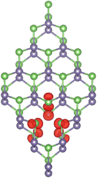 | ||
| Fig. 3 Spin density (iso-surface value: 0.005 e Å−3) in the GeAs monolayer with a pair of Ge vacancies. | ||
Fig. 4 shows the computed spin-polarized band structures of the GeAs monolayer with the presence of Ge vacancies. It can be observed clearly that the band structure of the VaGe system is spin-symmetric, corresponding to its non-magnetic nature. Meanwhile, a pair of Ge vacancies induce significant spin polarization in the band structure. Compared with that of the perfect monolayer, one can see new middle-gap energy branches to determine the electronic nature. Specifically, a single Ge vacancy leads to the metallization of the GeAs monolayer, meanwhile the feature-rich half-metallicity is obtained by pair Ge vacancies. In the latter case, the spin-up state is metallized, meanwhile the spin-down state exhibits a semiconductor character with an energy gap of 0.33 eV. These results suggest the pVaGe system to be a prospective 2D spintronic material, such that creating a pair of Ge vacancies can be considered as an efficient approach to functionalize the GeAs monolayer for spintronic applications.59
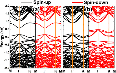 | ||
| Fig. 4 Spin-polarized band structure (the Fermi level is set to 0 eV) of the GeAs monolayer with (a) a single Ge vacancy and (b) a pair of Ge vacancies. | ||
To provide more insights into the electronic and magnetic properties of VaGe and pVaGe systems, PDOS spectra of As and Ge atoms closest to the defect sites are given in Fig. 5. From panel a, one can see that the metallic nature of the VaGe system is derived mainly from As-px,y,z states, while the Ge-s state gives rise to mainly new energy branches above the Fermi level. In the latter one, a small contribution from the As-pz state is also noted. Otherwise, the electronic and magnetic properties of the pVaGe system are regulated mainly by As-px,y,z states considering its high weight at the vicinity of the Fermi level in both spin channels with a strong spin polarization (see panel b).
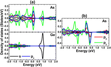 | ||
| Fig. 5 Projected density of states of atoms closest to defect sites in the GeAs monolayer with (a) a single Ge vacancy and (b) a pair of Ge vacancies. | ||
3.3 Effects of doping a single transition metal atom
Herein, the effects of doping with single transition metals (TMs) at the Ge site (V – VGe system, Cr – CrGe system, Mn – MnGe system, and Fe – FeGe system) on the electronic and magnetic properties of the GeAs monolayer are investigated. First, doping energy Ed and cohesive energy Ec are calculated using the following expressions: | (3) |
 | (4) |
Our spin-polarized calculations assert significant magnetization of the GeAs monolayer induced by doping with transition metals. Consequently, total magnetic moments of 2.94, 2.00, 3.00, and 4.00 μB are obtained for V-, Cr-, Mn, and Fe-doped systems, respectively. Herein, the local magnetic moments of V, Cr, Mn, and Fe impurities are 2.53, 3.38, 3.80, and 3.36 μB, respectively. Large local magnetic moments indicate the key role of TM atoms in generating the system magnetism. This feature is further confirmed by the spin density as illustrated in Fig. 6. From the figure, one can see that the difference in charge density between spin states – that is the origin of magnetism – takes place mainly at impurity sites. Therefore, it can be concluded that the magnetic properties are produced mainly by transition metals.
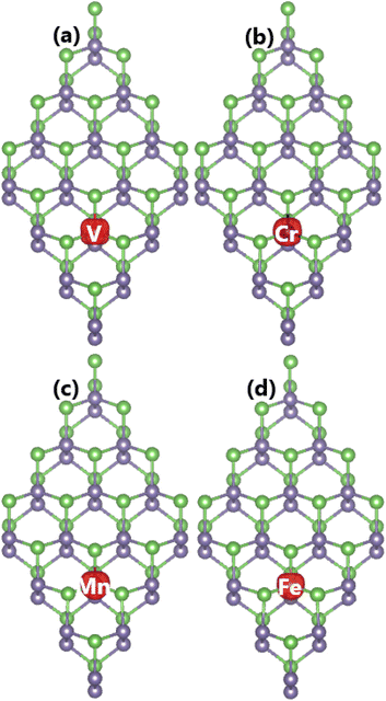 | ||
| Fig. 6 Spin density (iso-surface value: 0.02 e Å−3) in (a) V-, (b) Cr-, (c) Mn-, and (d) Fe-doped GeAs monolayers. | ||
Fig. 7 shows the spin-polarized band structures of the doped GeAs systems, where strong spin polarization is observed in all cases. It is undoubted that the magnetism with unbalanced spin-dependent charge density is reflected in the spin-polarized profile. Note that the electronic nature of the doped GeAs systems is determined by new middle-gap energy branches that appear in the vicinity of the Fermi level as a consequence of doping. Specifically, the half-metallicity is induced by doping with V, Mn, and Fe atoms. In these cases, one spin state is metallized, meanwhile the other exhibits the semiconductor character with energy gaps of 1.10, 1.17, and 0.87 eV, respectively. Moreover, the Cr-doped system can be classified as a diluted magnetic semiconductor material with spin-up and spin-down band gaps of 1.14 and 0.44 eV, respectively. Because of their metallic nature with the lowly electronegative character, TM impurities act as charge losers when they are substitutionally incorporated into the host GeAs monolayer. This process is further quantified by the Bader charge analysis, which indicates the transfer of 0.97, 0.71, 0.62, and 0.41 e from V, Cr, Mn, and Fe dopants to the host monolayer, respectively.
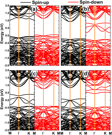 | ||
| Fig. 7 Spin-polarized band structure (the Fermi level is set to 0 eV) of (a) V-, (b) Cr-, (c) Mn-, and (d) Fe-doped GeAs monolayers. | ||
The contribution of TM impurities to form the band structure is further analyzed by their PDOS spectra displayed in Fig. 8. Focusing on the region around the Fermi level, the main contribution from the TM-3d orbital can be noted. The spin metallic character of the V-, Mn-, and Fe systems is derived mainly from V-dpz, Mn-dpz, and Fe-dpz states, respectively. Importantly, the spin polarization suggests also that magnetic properties are produced mainly by the 3d electrons of transition metal impurities.
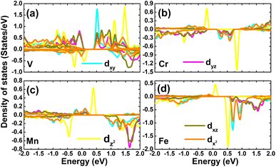 | ||
| Fig. 8 Projected density of states of transition metals in (a) V-, (b) Cr-, (c) Mn-, and (d) Fe-doped GeAs monolayers. | ||
3.4 Effects of doping a pair of transition metal atoms
Now, the effects of doping with a pair of TMs (pTMGe system) on the electronic and magnetic properties of the GeAs monolayer are investigated. First, the spin alignment between TM dopants is determined using the criterion of the lowest energy. Herein, parallel and antiparallel orientations are considered, as illustrated in Fig. 9. It is found that the ferromagnetism with a total magnetic moment of 4.00 μB is energetically favorable in the V-doped system with an energy of 608.3 meV smaller than that of the antiferromagnetism. In contrast, the antiferromagnetic state with zero total magnetic moment is more stable than the ferromagnetic state in the Cr-, Mn-, and Fe-doped GeAs monolayer. In these cases, the differences in energy are 1423.7, 1146.6, and 513.1 meV, respectively. From now on, only the stable states are investigated. Applying eqn (3), Ed values of 1.31, 1.25, 2.17, and 1.37 eV per atom are obtained for a pair of V, Cr, Mn, and Fe atoms, respectively. Except for the cases of Fe impurities, a higher doping level may require more energy to realize the doping process. Once formed, all pV-, pCr-, pMn-, and pFe-doped systems are structurally and chemically stable considering their negative Ec values of −3.45, −3.36, −3.37, and −3.45 eV per atom, respectively, which have been calculated using eqn (4).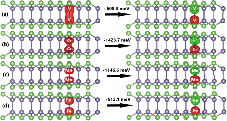 | ||
| Fig. 9 Spin density (iso-surface value: 0.02 e Å−3; positive spin value: red surface; negative spin value: green surface) in (a) pV-, (b) pCr-, (c) pMn-, and (d) pFe-doped GeAs monolayers. | ||
The computed spin-polarized band structures of the GeAs monolayer doped with a pair of transition metals are displayed in Fig. 10. Note that the ferromagnetism of the pV-doped system corresponds to its spin-polarized band structure that indicates the half-metallic nature. Herein, new middle-gap states appear to metallize the spin-down state, meanwhile the semiconductor spin-down state has an energy gap of 1.19 eV. In contrast, the band structures of pCr-, pMn-, and pFe-doped systems are spin-symmetric. A pair of Mn impurities leads to the emergence of the antiferromagnetic metallic nature, meanwhile the antiferromagnetic semiconductor behavior is induced in the GeAs monolayer by doping with a pair of Cr and Fe atoms, respectively. In the latter cases, energy gaps of 0.17 and 0.57 eV are obtained, respectively. Further, our Bader charge analysis indicates that each V atom transfers a charge quantity of 0.75 e to the host monolayer. In the antiferromagnetic systems, the atoms with a positive spin value transfer a larger amount of charge to the host monolayer than those with a negative spin value. Specifically, the host GeAs monolayer attracts charge quantities of 0.57/0.41, 0.54/0.37, and 0.31/0.20 e from Cr(+)/Cr(−), Mn(+)/Mn(−), and Fe(+)/Fe(−) atoms, respectively.
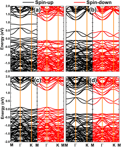 | ||
| Fig. 10 Spin-polarized band structure (the Fermi level is set to 0 eV) of (a) pV-, (b) pCr-, (c) pMn-, and (d) pFe-doped GeAs monolayers. | ||
Now, PDOS spectra of a pair of TM impurities are given in Fig. 11 to investigate in more detail the origin of electronic and magnetic properties. Due to the structural symmetry, PDOS spectra of V atoms are identical, meanwhile those of Cr–Mn–Fe atoms are asymmetric. Note that the metallic spin-up state of the pV-doped system is derived mainly from V-dxy − dxz − dx2 states. Similarly, Mn-dxy + dx2 and Mn-dxz + dyz states metallize the spin-up and spin-down states of the GeAs monolayer. Importantly, the strong spin polarization demonstrates the key role of TMs-3d electrons in generating the system magnetism.
 | ||
| Fig. 11 Projected density of states of transition metals (“+”: positive spin density value; “–”: negative spin density value) in (a) pV-, (b) pCr-, (c) pMn-, and (d) pFe-doped GeAs monolayers. | ||
4. Conclusions
To conclude, a systematic study has been carried out to clarify the effects of Ge vacancies and doping with transition metals on the electronic and magnetic properties of the GeAs monolayer. Theoretical calculations confirm the good dynamical, thermal, and mechanical stability of the GeAs monolayer. Ge–As bonds exhibit a mix of covalent (generated by the electronic hybridization between Ge-pz and As-pz states) and ionic (generated by the charge transfer from the Ge atom to the As atom) characters, while the Ge–Ge bond is predominantly covalent. The monolayer is significantly magnetized by creating a pair of Ge vacancies, where magnetic properties are produced mainly by the px,y,z states of As atoms around the defect sites. Meanwhile, the non-magnetic nature is preserved upon creating a single Ge vacancy, where As-px,y,z states induce the metallic behavior. Significant magnetism is also achieved by doping with transition metals, which is produced mainly by TMs-3d electrons. Moreover, the 3d orbital develops new middle-gap states to control either the half-metallicity or diluted magnetic semiconductor nature, which is desirable for spintronic applications. Further investigations indicate the ferromagnetic half-metallicity induced by doping with a pair of V atoms. Meanwhile antiferromagnetic metallic/semiconductor characters are obtained in the pMn-/pCr(pFe)-doped GeAs monolayer. Because of the structural symmetry, a zero total magnetic moment is obtained in the antiferromagnetic systems, meanwhile that of the pV-doped system is 4.00 μB contributed equally by V atoms. Our work may pave solid ways to achieve proper magnetization of the non-magnetic GeAs monolayer, from which new half-metallic or diluted magnetic semiconductor materials are obtained towards spintronic applications.Data availability
Data related to this study are available upon reasonable request.Conflicts of interest
The authors declare that they have no known competing financial interests or personal relationships that could have appeared to influence the work reported in this paper.Acknowledgements
Calculations were performed in the DGCTIC-UNAM Supercomputing Center (projects LANCAD-UNAM-DGTIC-368). D. M. Hoat expresses his gratitude for all the valuable support from Duy Tan University, which is going to celebrate its 30th anniversary of establishment (Nov. 11, 1994–Nov. 11, 2024) towards ”Integral, Sustainable and Stable Development”.References
- J. Wang, G. Chen, H. Jiang, Z. Li and X. Wang, Advances in nano-scaled biosensors for biomedical applications, Analyst, 2013, 138(16), 4427–4435 RSC.
- A. Kraytsberg and Y. Ein-Eli, The impact of nano-scaled materials on advanced metal–air battery systems, Nano Energy, 2013, 2(4), 468–480 CrossRef CAS.
- J. A. Rodríguez-Jiménez, E. Díaz-Cervantes, F. Aguilera-Granja and J. Robles, Computational study of GanAsm (m + n = 2–9) clusters using DFT calculations, J. Nanopart. Res., 2019, 21, 1–14 CrossRef.
- J. A. Rodríguez-Jiménez, F. Aguilera-Granja, J. Robles and A. Vega, On the doping of the Ga12As12 cluster with groups p and d atomic impurities, Theor. Chem. Acc., 2021, 140(12), 160 Search PubMed.
- K. S. Novoselov, A. K. Geim, S. V. Morozov, D.-e. Jiang, Y. Zhang, S. V. Dubonos, I. V. Grigorieva and A. A. Firsov, Electric field effect in atomically thin carbon films, science, 2004, 306(5696), 666–669 CrossRef CAS PubMed.
- C. Soldano, A. Mahmood and E. Dujardin, Production, properties and potential of graphene, Carbon, 2010, 48(8), 2127–2150 CrossRef CAS.
- D. R. Cooper, B. D’Anjou, N. Ghattamaneni, B. Harack, M. Hilke, A. Horth, N. Majlis, M. Massicotte, L. Vandsburger and E. Whiteway, et al., Experimental review of graphene, Int. Scholarly Res. Not., 2011, 2012, 501686 Search PubMed.
- Y. Yang, H. Hou, G. Zou, W. Shi, H. Shuai, J. Li and X. Ji, Electrochemical exfoliation of graphene-like two-dimensional nanomaterials, Nanoscale, 2019, 11(1), 16–33 RSC.
- E. Gao, S.-Z. Lin, Z. Qin, M. J. Buehler, X.-Q. Feng and Z. Xu, Mechanical exfoliation of two-dimensional materials, J. Mech. Phys. Solids, 2018, 115, 248–262 CrossRef CAS.
- J. Zhang, F. Wang, V. B. Shenoy, M. Tang and J. Lou, Towards controlled synthesis of 2D crystals by chemical vapor deposition (CVD), Mater. Today, 2020, 40, 132–139 CrossRef CAS.
- Z. Cai, B. Liu, X. Zou and H.-M. Cheng, Chemical vapor deposition growth and applications of two-dimensional materials and their heterostructures, Chem. Rev., 2018, 118(13), 6091–6133 CrossRef CAS PubMed.
- M. Nakano, Y. Wang, Y. Kashiwabara, H. Matsuoka and Y. Iwasa, Layer-by-layer epitaxial growth of scalable WSe2 on sapphire by molecular beam epitaxy, Nano Lett., 2017, 17(9), 5595–5599 CrossRef CAS PubMed.
- D. Zhou, H. Li, N. Si, H. Li, H. Fuchs and T. Niu, Epitaxial growth of main group monoelemental 2D materials, Adv. Funct. Mater., 2021, 31(6), 2006997 CrossRef CAS.
- X. J. Lee, B. Y. Z. Hiew, K. C. Lai, L. Y. Lee, S. Gan, S. Thangalazhy-Gopakumar and S. Rigby, Review on graphene and its derivatives: Synthesis methods and potential industrial implementation, J. Taiwan Inst. Chem. Eng., 2019, 98, 163–180 CrossRef CAS.
- J. Sturala, J. Luxa, M. Pumera and Z. Sofer, Chemistry of graphene derivatives: Synthesis, applications, and perspectives, Chem.–Eur. J., 2018, 24(23), 5992–6006 CrossRef CAS PubMed.
- K. K. Kim, A. Hsu, X. Jia, S. M. Kim, Y. Shi, M. Hofmann, D. Nezich, J. F. Rodriguez-Nieva, M. Dresselhaus and T. Palacios, et al., Synthesis of monolayer hexagonal boron nitride on Cu foil using chemical vapor deposition, Nano Lett., 2012, 12(1), 161–166 CrossRef PubMed.
- A. E. Naclerio and P. R. Kidambi, A review of scalable hexagonal boron nitride (h-BN) synthesis for present and future applications, Adv. Mater., 2023, 35(6), 2207374 CrossRef CAS PubMed.
- R. Lv, J. A. Robinson, R. E. Schaak, D. Sun, Y. Sun, T. E. Mallouk and M. Terrones, Transition metal dichalcogenides and beyond: synthesis, properties, and applications of single-and few-layer nanosheets, Acc. Chem. Res., 2015, 48(1), 56–64 CrossRef CAS PubMed.
- M. Bosi, Growth and synthesis of mono and few-layers transition metal dichalcogenides by vapour techniques: a review, RSC Adv., 2015, 5(92), 75500–75518 RSC.
- L. Tao, E. Cinquanta, D. Chiappe, C. Grazianetti, M. Fanciulli, M. Dubey, A. Molle and D. Akinwande, Silicene field-effect transistors operating at room temperature, Nat. Nanotechnol., 2015, 10(3), 227–231 CrossRef CAS PubMed.
- L. Li, Y. Yu, G. J. Ye, Q. Ge, X. Ou, H. Wu, D. Feng, X. H. Chen and Y. Zhang, Black phosphorus field-effect transistors, Nat. Nanotechnol., 2014, 9(5), 372–377 CrossRef CAS PubMed.
- W. Zhang, H. Enriquez, Y. Tong, A. Bendounan, A. Kara, A. P. Seitsonen, A. J. Mayne, G. Dujardin and H. Oughaddou, Epitaxial synthesis of blue phosphorene, Small, 2018, 14(51), 1804066 CrossRef PubMed.
- Y. Mogulkoc, H. Guler, B. Tokmakci and R. Caglayan, Comprehensive study on electronic structures of SiGe/Ga2SeTe vdW heterobilayer, J. Mater. Sci., 2023, 58(9), 4020–4030 CrossRef CAS.
- H. Zheng, X.-B. Li, N.-K. Chen, S.-Y. Xie, W. Q. Tian, Y. Chen, H. Xia, S. Zhang and H.-B. Sun, Monolayer II–VI semiconductors: A first-principles prediction, Phys. Rev. B: Condens. Matter Mater. Phys., 2015, 92(11), 115307 CrossRef.
- J. Cheng, C. Wang, X. Zou and L. Liao, Recent advances in optoelectronic devices based on 2D materials and their heterostructures, Adv. Opt. Mater., 2019, 7(1), 1800441 CrossRef.
- J. Shim, H.-Y. Park, D.-H. Kang, J.-O. Kim, S.-H. Jo, Y. Park and J.-H. Park, Electronic and optoelectronic devices based on two-dimensional materials: From fabrication to application, Adv. Electron. Mater., 2017, 3(4), 1600364 CrossRef.
- Y. Xue, Q. Zhang, W. Wang, H. Cao, Q. Yang and L. Fu, Opening two-dimensional materials for energy conversion and storage: a concept, Adv. Energy Mater., 2017, 7(19), 1602684 CrossRef.
- X. Zhang, L. Hou, A. Ciesielski and P. Samorì, 2D materials beyond graphene for high-performance energy storage applications, Adv. Energy Mater., 2016, 6(23), 1600671 CrossRef.
- T. Dong, J. Simões and Z. Yang, Flexible photodetector based on 2D materials: processing, architectures, and applications, Adv. Mater. Interfaces, 2020, 7(4), 1901657 CrossRef CAS.
- Z. Sun and H. Chang, Graphene and graphene-like two-dimensional materials in photodetection: mechanisms and methodology, ACS Nano, 2014, 8(5), 4133–4156 CrossRef CAS PubMed.
- S. Yang, C. Jiang and S.-h. Wei, Gas sensing in 2D materials, Appl. Phys. Rev., 2017, 4(2), 021304 Search PubMed.
- B. Wang, Y. Gu, L. Chen, L. Ji, H. Zhu and Q. Sun, Gas sensing devices based on two-dimensional materials: a review, Nanotechnology, 2022, 33(25), 252001 CrossRef CAS PubMed.
- D. Deng, K. Novoselov, Q. Fu, N. Zheng, Z. Tian and X. Bao, Catalysis with two-dimensional materials and their heterostructures, Nat. Nanotechnol., 2016, 11(3), 218–230 CrossRef CAS PubMed.
- X. Chia and M. Pumera, Characteristics and performance of two-dimensional materials for electrocatalysis, Nat. Catal., 2018, 1(12), 909–921 CrossRef CAS.
- Y. Liu, C. Zeng, J. Zhong, J. Ding, Z. M. Wang and Z. Liu, Spintronics in two-dimensional materials, Nano–Micro Lett., 2020, 12, 1–26 CrossRef PubMed.
- W. Han, Perspectives for spintronics in 2D materials, APL Mater., 2016, 4(3), 032401 CrossRef.
- C. Barreteau, B. Michon, C. Besnard and E. Giannini, High-pressure melt growth and transport properties of SiP, SiAs, GeP, and GeAs 2D layered semiconductors, J. Cryst. Growth, 2016, 443, 75–80 CrossRef CAS.
- J. Guo, Y. Liu, Y. Ma, E. Zhu, S. Lee, Z. Lu, Z. Zhao, C. Xu, S.-J. Lee and H. Wu, et al., Few-layer GeAs field-effect transistors and infrared photodetectors, Adv. Mater., 2018, 30(21), 1705934 CrossRef PubMed.
- Z. Zhou, M. Long, L. Pan, X. Wang, M. Zhong, M. Blei, J. Wang, J. Fang, S. Tongay and W. Hu, et al., Perpendicular optical reversal of the linear dichroism and polarized photodetection in 2D GeAs, ACS Nano, 2018, 12(12), 12416–12423 CrossRef CAS PubMed.
- A. Di Bartolomeo, A. Grillo, F. Giubileo, L. Camilli, J. Sun, D. Capista and M. Passacantando, Field emission from two-dimensional GeAs, J. Phys. D: Appl. Phys., 2020, 54(10), 105302 CrossRef.
- B. Mortazavi, M. Shahrokhi, G. Cuniberti and X. Zhuang, Two-dimensional SiP, SiAs, GeP and GeAs as promising candidates for photocatalytic applications, Coatings, 2019, 9(8), 522 CrossRef CAS.
- A. Hirohata, K. Yamada, Y. Nakatani, I.-L. Prejbeanu, B. Diény, P. Pirro and B. Hillebrands, Review on spintronics: Principles and device applications, J. Magn. Magn. Mater., 2020, 509, 166711 CrossRef CAS.
- I. Žutić, J. Fabian and S. D. Sarma, Spintronics: Fundamentals and applications, Rev. Mod. Phys., 2004, 76(2), 323 CrossRef.
- Y. Liu, C. Xiao, Z. Li and Y. Xie, Vacancy engineering for tuning electron and phonon structures of two-dimensional materials, Adv. Energy Mater., 2016, 6(23), 1600436 CrossRef.
- S. Yu, J. Tang, Y. Wang, F. Xu, X. Li and X. Wang, Recent advances in two-dimensional ferromagnetism: strain-, doping-, structural-and electric field-engineering toward spintronic applications, Sci. Technol. Adv. Mater., 2022, 23(1), 140–160 CrossRef PubMed.
- W. Kohn and L. J. Sham, Self-consistent equations including exchange and correlation effects, Phys. Rev., 1965, 140(4A), A1133 CrossRef.
- G. Kresse and J. Furthmüller, Efficiency of ab initio total energy calculations for metals and semiconductors using a plane-wave basis set, Comput. Mater. Sci., 1996, 6(1), 15–50 CrossRef CAS.
- G. Kresse and J. Furthmüller, Efficient iterative schemes for ab initio total-energy calculations using a plane-wave basis set, Phys. Rev. B: Condens. Matter Mater. Phys., 1996, 54(16), 11169 CrossRef CAS PubMed.
- J. P. Perdew, K. Burke and M. Ernzerhof, Generalized gradient approximation made simple, Phys. Rev. Lett., 1996, 77(18), 3865 CrossRef CAS PubMed.
- S. L. Dudarev, G. A. Botton, S. Y. Savrasov, C. Humphreys and A. P. Sutton, Electron-energy-loss spectra and the structural stability of nickel oxide: An LSDA + U study, Phys. Rev. B, 1998, 57(3), 1505 CrossRef CAS.
- Y. Wang, S. Li and J. Yi, Transition metal-doped tin monoxide monolayer: a first-principles study, J. Phys. Chem. C, 2018, 122(8), 4651–4661 CrossRef CAS.
- S. Grimme, J. Antony, S. Ehrlich and H. Krieg, A consistent and accurate ab initio parametrization of density functional dispersion correction (DFT-D) for the 94 elements H-Pu, J. Chem. Phys., 2010, 132(15), 154104 CrossRef PubMed.
- H. J. Monkhorst and J. D. Pack, Special points for Brillouin-zone integrations, Phys. Rev. B: Condens. Matter Mater. Phys., 1976, 13(12), 5188 CrossRef.
- A. Togo, L. Chaput, T. Tadano and I. Tanaka, Implementation strategies in phonopy and phono3py, J. Phys.: Condens.Matter, 2023, 35(35), 353001, DOI:10.1088/1361-648X/acd831.
- S. Nosé, A unified formulation of the constant temperature molecular dynamics methods, J. Chem. Phys., 1984, 81(1), 511–519 CrossRef.
- W. G. Hoover, Canonical dynamics: Equilibrium phase-space distributions, Phys. Rev. A, 1985, 31(3), 1695 CrossRef PubMed.
- F. Mouhat and F.-X. Coudert, Necessary and sufficient elastic stability conditions in various crystal systems, Phys. Rev. B: Condens. Matter Mater. Phys., 2014, 90(22), 224104 CrossRef.
- A. V. Krukau, O. A. Vydrov, A. F. Izmaylov and G. E. Scuseria, Influence of the exchange screening parameter on the performance of screened hybrid functionals, J. Chem. Phys., 2006, 125(22), 224106 CrossRef PubMed.
- X. Li and J. Yang, First-principles design of spintronics materials, Natl. Sci. Rev., 2016, 3(3), 365–381 CrossRef CAS.
Footnote |
| † Electronic supplementary information (ESI) available. See DOI: https://doi.org/10.1039/d4na00235k |
| This journal is © The Royal Society of Chemistry 2024 |

