DOI:
10.1039/D4NA00304G
(Paper)
Nanoscale Adv., 2024,
6, 4128-4136
Large piezoelectric responses and ultra-high carrier mobility in Janus HfGeZ3H (Z = N, P, As) monolayers: a first-principles study
Received
11th April 2024
, Accepted 13th June 2024
First published on 14th June 2024
Abstract
Breaking structural symmetry in two-dimensional layered Janus materials can result in enhanced new phenomena and create additional degrees of piezoelectric responses. In this study, we theoretically design a series of Janus monolayers HfGeZ3H (Z = N, P, As) and investigate their structural characteristics, crystal stability, piezoelectric responses, electronic features, and carrier mobility using first-principles calculations. Phonon dispersion analysis confirms that HfGeZ3H monolayers are dynamically stable and their mechanical stability is also confirmed through the Born–Huang criteria. It is demonstrated that while HfGeN3H is a semiconductor with a large bandgap of 3.50 eV, HfGeP3H and HfGeAs3H monolayers have narrower bandgaps being 1.07 and 0.92 eV, respectively. When the spin–orbit coupling is included, large spin-splitting energy is found in the electronic bands of HfGeZ3H. Janus HfGeZ3H monolayers can be treated as piezoelectric semiconductors with the coexistence of both in-plane and out-of-plane piezoelectric responses. In particular, HfGeZ3H monolayers exhibit ultra-high electron mobilities up to 6.40 × 103 cm2 V−1 s−1 (HfGeAs3H), indicating that they have potential for various applications in nanoelectronics.
1 Introduction
The piezoelectric property of materials demonstrates the ability to convert energy effectively from electrical to mechanical energy and vice versa. This property is attracting the attention of scientists due to its applications in various fields, such as sensors, nanogenerators, and medical devices.1–3 The correlation between piezoelectricity and the symmetry of the crystal structure is widely recognized.4 A material is classified as piezoelectric when it possesses a non-centrosymmetric crystal structure. Recent studies have shown that 2D nanomaterials have great potential for application in piezoelectric devices because they possess strong piezoelectric effects.5,6
In parallel with the search for new 2D structures, scientists have succeeded in creating asymmetric Janus structures based on known symmetric 2D structures, i.e. successfully synthesizing Janus MoSSe sheets.7,8 The successful fabrication of 2D Janus materials has provided us with a new approach to studying 2D structures. As a consequence, many Janus structures have been proposed and studied systematically.9–12 Due to the lack of vertical symmetry, Janus structures possess many outstanding physical characteristics compared to their original symmetric structures.13–16 Janus materials show diverse application prospects in various fields, such as electronics, optoelectronics, thermoelectrics, and water-splitting catalysts.17–20 In particular, 2D Janus materials exhibit adherence to the non-centrosymmetric requirement, hence demonstrating their potential as piezoelectric materials.21–24 The piezoelectric effect was predicted in the MoS2 monolayer6 and was later confirmed experimentally.25,26 Group IV monochalcogenides have shown strong piezoelectric responses with a piezoelectric coefficient of 251 pm V−1.27 The piezoelectric effect has also been found in Janus group III chalcogenide monolayers with an in-plane piezoelectric coefficient of up to 8.47 pm V−1.28 Besides, the reduction of mirror symmetry in the Janus structure gives rise to vertical polarization, leading to enhanced out-of-plane piezoelectricity.28 Very recently, the piezoelectric effect has been reported in other 2D Janus materials, such as γ-Sn2XY (X/Y = S, Se, Te)29 or WSiZ3H (Z = N, P, As).30
Very recently, a MoSi2N4 sheet was successfully experimentally fabricated,31 paving the way for a new 2D family, called the MA2Z4 family,32 with many interesting application prospects. Soon after, many MA2Z4-based Janus structures were proposed, including XMoSiN2 (X = S, Se, Te)33 and MGeSiP4 (M = Ti, Zr, Hf).34 Many novel physical properties have been reported in MA2Z4-based Janus materials.35–37 In this study, we propose the 2D Janus HfGeZ3H (Z = N, P, As) monolayers and systematically investigate their crystal structure characteristics, electronic states, elasticity, and piezoelectric responses as well as the mobility of carriers.
2 Calculation details
The Vienna ab initio simulation package38,39 was utilized to perform first-principles calculations based on the projector augmented wave approach.40,41 The electron exchange–correlation functional was treated using the generalized gradient approximation parameterized using the Perdew, Burke, and Ernzerhof (PBE) functional.42 The hybrid functional suggested by Heyd, Scuseria, and Ernzerhof (HSE06) was employed to enhance the precision of electronic band gap analysis.43 The semiempirical DFT-D3 technique was applied for the weak van der Waals forces, which may be available in the layered material.44 Spin–orbit coupling (SOC) was incorporated into the self-consistent computations in order to examine the consequences of SOC.45 The plane wave basis set's energy cutoff was set at 650 eV and a 12 × 12 × 1 k-point mesh grid was used to sample the Brillouin zone integration. Atom positions in the crystal were totally relaxed until the forces on each atom were lower than 1 × 10⁻³ eV Å−1. The energy convergence threshold was chosen to be 1 × 10⁻⁶ eV. A 35 Å vacuum space was inserted into the vertical axis to reduce the interlayer interactions. We used the frozen-phonon technique as performed using the PHONOPY code to compute the phonon spectra.46 The thermal stability of the investigated structures was examined via ab initio molecular dynamics (AIMD) simulations at a constant temperature of 300 K with a canonical ensemble within 10 ps (time step of 1 fs). To rectify the dipole moment built in the asymmetric material, we added the dipole correction to our calculation. The elasticity and piezoelectricity were investigated using the strain–stress relationships and density functional perturbation theory (DFPT). The deformation potential technique was employed in order to examine carrier mobility in the studied structures.47
3 Results and discussion
3.1 Crystal structure and stability
The optimized crystal structure of the Janus HfGeZ3H (Z = N, P, As) monolayers is shown in Fig. 1. The unit cell of Janus HfGeZ3H, as denoted by the rhombus in Fig. 1(a), consists of six atoms, including three Z atoms, one H atom, one Hf atom, and one Ge atom. It is calculated that the lattice parameter a of HfGeZ3H is from 3.16 to 3.88 Å, which depends on the atomic size of the Z element. Due to the small atomic size of N compared with P and As the values of the structural parameters of HfGeN3H are much lower than those of HfGeP3H and HfGeAs3H as revealed in Table 1. The lattice parameters for the Janus HfGeZ3H monolayers are comparable to those of HfGe2Z4.32
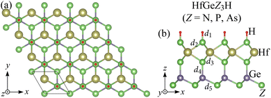 |
| | Fig. 1 Crystal structures of Janus HfGeZ3H (Z = N, P, As) monolayers in the (a) top and (b) side views. | |
Table 1 Lattice constant a (Å), thickness h (Å) bond length d (Å), cohesive energy Ecoh (eV per atom), and Bader charger q (|e|) of atoms for Janus HfGeZ3H monolayers
|
|
a
|
h
|
d
1
|
d
2
|
d
3
|
d
4
|
d
5
|
E
coh
|
q
Hf
|
q
Ge
|
q
Z1
|
q
Z2
|
q
Z3
|
q
H
|
| HfGeN3H |
3.16 |
5.88 |
1.02 |
2.18 |
2.19 |
1.87 |
1.91 |
−7.28 |
−1.933 |
−1.577 |
1.067 |
1.406 |
1.128 |
−0.092 |
| HfGeP3H |
3.74 |
7.65 |
1.42 |
2.60 |
2.60 |
2.31 |
2.39 |
−6.47 |
−0.731 |
−0.010 |
−0.206 |
0.493 |
−0.051 |
0.506 |
| HfGeAs3H |
3.88 |
8.05 |
1.53 |
2.70 |
2.69 |
2.42 |
2.50 |
−5.05 |
−0.631 |
−0.070 |
−0.306 |
0.555 |
−0.107 |
0.558 |
To evaluate the possibility of Janus HfGeZ3H monolayers being fabricated experimentally, we investigated their stability by calculating their phonon dispersion and cohesive energies. Fig. 2(a) presents the phonon spectra of all examined compounds. It is indicated that there are 18 vibrational branches in the Brillouin zone due to the presence of six atoms in the unit cell. As shown in Fig. 2(a), there are certain frequency ranges where the optical modes and acoustic modes coexist, which could result in strong acoustic-optical scattering in the studied structures. Besides, we can observe a large distinct phononic gap in the optical region in the phonon dispersion of Janus HfGeZ3H monolayers. This is due to the large difference in mass between the constituent elements in the examined compounds. Notably, the vibrational branches all contain real frequencies in the whole first Brillouin zone, reflecting the dynamically stable structure of these Janus monolayers. Furthermore, we performed AIMD simulations to verify the thermal stability of the examined structures at room temperature. The calculated results for the variations in the temperature during AIMD simulation of HfGeZ3H monolayers are revealed in Fig. 2(b). It is indicated that the temperature fluctuations are small at around 300 K and the crystal structures of HfGeZ3H remain robust throughout the 10 ps of AIMD simulation. There is neither chemical bond breaking nor structural phase transition during AIMD simulation. These support the hypothesis that the HfGeZ3H monolayers are thermally stable. Indeed, we explore the cohesive energy to examine the bond strength between atoms in the Janus configurations. Cohesive energy per atom is determined according to the following formula:
| |  | (1) |
where
Etot denotes the total energy of Janus HfGeZ
3H;
EHf,
EGe,
EH, and
EZ are the energies of single atoms Hf, Ge, H, and Z, respectively.
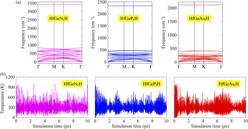 |
| | Fig. 2 Phonon dispersion (a) and variations of temperature during AIMD simulation at room temperature (b) of Janus HfGeN3H, HfGeP3H, and HfGeAs3H monolayers. | |
Our computed results show that the cohesive energy, which is calculated using eqn (1), has a negative value, as presented in Table 1, confirming the energetic stability of the examined monolayers. The values of Ecoh are calculated to be −7.28, −6.47, and −5.05 eV per atom for HfGeN3H, HfGeP3H, and HfGeAs3H, respectively. Thus, the most energetically stable structure is HfGeN3H. This is consistent with the fact that the shorter the chemical bonds, the stronger the bond. Furthermore, we also carry out a Bader charge analysis to get insight into the charge transfer between the atoms in the considered compounds. In Table 1, we report the computed results for the atomic Bader charges. It is easy to see that the H atom loses a small amount of charge in the 2D compound HfGeN3H. For the other compounds, most of the effective electrons move to the H atom. Besides, we observe that the Hf and Ge atoms lose their charges.
3.2 Electronic characteristics
We here discover the intriguing electronic features of the 2D HfGeZ3H systems. We first explore the band structures of HfGeZ3H as presented in Fig. 3. It is demonstrated that while HfGeN3H is a wide direct bandgap semiconductor, both HfGeP3H and HfGeAs3H are semiconductors with narrower indirect bandgaps. The calculated values for the bandgap of HfGeN3H, HfGeP3H, and HfGeAs3H are 2.28, 0.41, and 0.29 eV, respectively. Although the PBE method is a popular method for predicting the electronic characteristics of materials, this method is known to underestimate the accuracy of bandgaps of semiconductors and insulators as demonstrated by Perdew and Levy.48 The GW approximation49 or hybrid functionals, such as HSE06,43 are considered a suitable solution for tuning the band diagrams of semiconductors. At the HSE06 theoretical level, the bandgaps of HfGeN3H, HfGeP3H, and HfGeAs3H are predicted to be 3.50, 1.07, and 0.92 eV, respectively. It is clear that due to the larger atomic radii of P and As compared to N, there is a reduced overlap of atomic orbitals in HfGeP3H and HfGeAs3H, which results in their bandgaps being smaller than that of HfGeN3H. By using the PBE functional, the computed bandgaps of HfGeZ3H are much narrower than those evaluated by the HSE06 approach. The computed data for the bandgaps of HfGeZ3H are presented in Table 2.
 |
| | Fig. 3 Band structures of (a) HfGeN3H, (b) HfGeP3H, and (c) HfGeAs3H at the PBE and HSE06 theoretical levels. | |
Table 2 The PBE/HSE06/PBE + SOC bandgap Eg (eV), spin-splitting energy λc (eV), vacuum level difference ΔΦ (eV), and work function Φ of HfGeZ3H monolayers
|
|
E
PBEg
|
E
HSE06g
|
E
PBE+SOCg
|
λ
c
|
Δφ |
φ
H
|
φ
Z
|
| WSiN3H |
2.28 |
3.50 |
2.21 |
0.30 |
2.66 |
3.36 |
6.02 |
| WSiP3H |
0.41 |
1.07 |
0.36 |
0.26 |
0.68 |
2.70 |
3.38 |
| WSiAs3H |
0.29 |
0.92 |
0.17 |
0.36 |
0.19 |
2.68 |
2.87 |
When compounds are formed from heavy elements, the SOC significantly influences their electronic characteristics. The electronic landscape of 2D layered materials is enhanced by the SOC effect, which renders them adaptable to a variety of applications ranging from traditional electronics to cutting-edge domains such as valleytronics and spintronics. The SOC can remove the degeneracy of electronic states, leading to energy splitting in the electronic bands, and can also modify the band gap of the studied structures. The strength of SOC in 2D structures can be tuned in different ways, including structural modifications, particularly in structures with a lack of inversion symmetry. Enhanced SOC in 2D structures could be useful for applications in spintronic devices, where the spin degree of freedom is a key parameter for spintronics. To evaluate the influences of the SOC on the electronic features of HfGeZ3H, we determined their energy band structures using the PBE + SOC approach as depicted in Fig. 4. When the SOC is taken into account, spin degeneracy is eliminated and there is spin splitting in the band structure of the studied materials. It is shown that a large spin-splitting energy λc is found at the k point of the conduction band. The calculated value of λc for HfGeN3H, HfGeP3H, and HfGeAs3H is found to be 0.30, 0.26, and 0.36 eV respectively. In the presence of the SOC effect, the bandgap of HfGeZ3H is slightly reduced. The PBE + SOC bandgaps of HfGeN3H, HfGeP3H, and HfGeAs3H are respectively 2.21, 0.36, and 0.17 eV as revealed in Table 2.
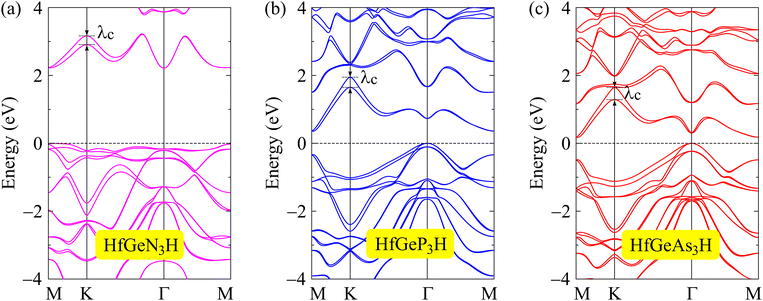 |
| | Fig. 4 Band structures computed by the PBE + SOC approach of (a) HfGeN3H, (b) HfGeP3H, and (c) HfGeAs3H monolayers. | |
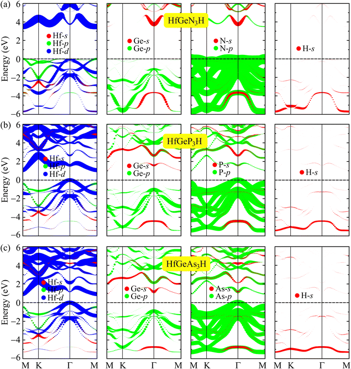
In Fig. 5, we reveal the weighted bands of HfGeZ3H to better see the contribution of atomic orbitals in the formation of their electronic band structure. As depicted in Fig. 5, we can see that the tendency to form the band structure is similar in all investigated monolayers. It is indicated that the conduction band minimum (CBM) of HfGeZ3H monolayers is mainly contributed by the Hf-d orbitals. Meanwhile, the p orbitals of the group V elements (N, P, and As) play a major role in forming the valence band, particularly around the valence band maximum (VBM). The Hf-d orbitals also have a significant contribution to the valence band near the Fermi level.
 |
| | Fig. 5 The PBE weighted bands of (a) HfGeN3H, (b) HfGeP3H, and (c) HfGeAs3H monolayers. | |
One of the essential electronic properties that we need to investigate is the electrostatic potential and work function. The work function tells us about the ability of electrons to escape from the material, and it depends on the vacuum level Ev and Fermi level Ef as φ = Ev − Ef. Since Janus structures have a vertically asymmetric crystal structure with atomic layers of different electronegativities, polarization exists along the vertical direction. In other words, the lack of mirror symmetry causes an out-of-plane polarization in the Janus structure. It should also be noted that large differences in electronegativity between the surfaces will directly affect the value of the out-of-plane piezoelectric constants. Therefore, when evaluating the electrostatic potential of Janus materials, we need to include the dipole correction in the calculations for the electrostatic potential. Fig. 6 shows the electrostatic potential of the investigated monolayers with dipole corrections. It is easy to recognize the asymmetry in the shape of the electrostatic potential, which is attributed to the structural asymmetry of Janus systems. Besides, because the sides of the Janus system are made up of different atoms, the vacuum levels on the two sides are also different, leading to unequal work functions on the two sides of the systems. It is calculated that the vacuum level difference Δφ between the two sides decreases as the Z element changes from N to As. The computed values for HfGeN3H, HfGeP3H, and HfGeAs3H are 2.66, 0.68, and 0.19 eV, respectively. The obtained values of the vacuum level difference and the work function at the two surfaces of the Janus material are detailed in Table 3. The calculation results reveal that the work functions at the two sides for the three HfGeZ3H systems go from 2.68 to 3.36 eV. Indeed, the values for the work function and the vacuum level difference gradually decrease with the increasing atomic number of element Z. In each given Janus system, the work function at the H surface is smaller than that at the Z side. In other words, it is more difficult for electrons to escape from the Z surface than from the H one.
 |
| | Fig. 6 Electrostatic potentials of (a) HfGeN3H, (b) HfGeP3H, and (c) HfGeAs3H monolayers. | |
Table 3 Elastic constants Cij (N m−1), Young's modulus Y2D (N m−1), Poisson's ratio ν, and piezoelectric coefficients e11 (10−10 C m−1), e31 (10−10 C m−1), d11 (pm V−1), and d31 (pm V−1) of Janus HfGeZ3H
|
|
C
11
|
C
12
|
C
66
|
Y
2D
|
ν
|
e
11
|
e
31
|
d
11
|
d
31
|
| HfGeN3H |
274.66 |
100.87 |
86.89 |
237.61 |
0.37 |
2.77 |
0.32 |
1.59 |
0.09 |
| HfGeP3H |
115.64 |
39.43 |
38.10 |
102.19 |
0.34 |
−0.65 |
0.14 |
−0.86 |
0.09 |
| HfGeAs3H |
100.67 |
37.87 |
31.40 |
86.42 |
0.38 |
−1.12 |
0.02 |
−1.78 |
0.01 |
3.3 Piezoelectric effect
Piezoelectricity is a crucial property of materials that enables the transformation of mechanical energy into electrical energy or vice versa. A piezoelectric semiconductor is subject to significant limitations due to its crystalline symmetry. The occurrence of piezoelectric effects is limited to structures that lack centrosymmetry. The piezoelectric features of HFGeZ3H materials can be attributed to their noncentrosymmetry, resulting in both in-plane and out-of-plane piezoelectric effects. Recent experimental measurements show good agreement between experimental results25 and previous DFT calculations6 for piezoelectric coefficients in 2D MoS2 monolayers. Piezoelectricity refers to the ground-state characteristics that are strongly associated with polarization. Therefore, DFT calculations have been demonstrated to be a reliable method for predicting piezoelectric coefficients.
Initially, we compute the elastic stiffness coefficients Cij, which are essential for determining the piezoelectric coefficients. Based on Cij, we can also evaluate the elastic stability as well as the basic mechanical characteristics of the material. The elastic stiffness coefficients Cij are determined using the energy–strain relationships. Here, the relaxed-ion coefficients, whose positions of the atoms were relaxed at each value of strain, are calculated. The relaxed-ion coefficients are anticipated to exhibit greater consistency with experimental measurements than the clamped-ion coefficients.6Table 2 summarizes our calculated results for the relaxed-ion elastic constants C11, C12, and C66. Importantly, the obtained values of Cij for HfGeZ3H satisfy the criterion for mechanical stabilities proposed by Born and Huang in 2D materials (C11 > 0 and C112 − C122 > 0),50,51 ensuring that our predicted Janus monolayers are mechanically stable. Based on the results of these elastic constants, we obtain Young's modulus Y2D and Poisson's ratio ν as follows:
| |  | (2) |
| |  | (3) |
Our results show that Janus compounds HfGeZ3H possess isotropic mechanical properties, which are attributed to their isotropic structure. Table 2 reveals that the Young's modulii of HfGeN3H, HfGeP3H, and HfGeAs3H are 237.61, 102.19, and 86.42 N m−1, respectively. Young's modulus of HfGeZ3H is comparable to that of MoGeZ3H;52 however, it is much smaller than that of graphene.53 It reflects that HfGeZ3H monolayers are predicted to be mechanically flexible structures.
The modern theory of polarization has revealed that the change in polarization eijk when uniaxial strain is applied is the basis for evaluating the linear piezoelectric coefficient dijk.54 In 2D materials, the linear piezoelectric effect may be understood as a first-order coupling between the surface polarization (Pi) and the strain (εjk) or stress (σjk) tensors. Here, i, j, k ∈ {1, 2, 3} and 1, 2, and 3 correspond respectively to x, y, and z.
The piezoelectric tensors eijk and dijk are third-rank tensors, which are evaluated according to the following expression:6
| |  | (4) |
| |  | (5) |
The crystallographic symmetry element is used to determine the degree of piezoelectric response in 2D materials. In the case of Janus asymmetric HfGeZ3H, which belongs to the point symmetry group P3m1, it simultaneously possesses in-plane (e11) and out-of-plane (e31) piezoelectric coefficients. We can calculate e11 and e31 by introducing uniaxial strain along the x axis of the orthorhombic supercell using the density functional perturbation theory. The coefficients dij are then calculated according to the expression:28
| |  | (6) |
| |  | (7) |
Table 2 presents the computed results of the piezoelectric coefficients of HfGeZ3ZH. The piezoelectric coefficient e11 is the largest in the Janus HfGeN3H monolayer (2.77 × 10⁻¹⁰ C m−1), while the magnitude of d11 is the largest in the HfGeAs3H monolayer (−1.78 pm V−1). These values are smaller than the corresponding piezoelectric coefficients in structurally similar compounds such as MoGeZ3H55 and WSiZ3H.56 More importantly, the out-of-plane piezoelectric coefficients in Janus structures are non-zero, resulting from the breaking of mirror symmetry due to different atoms at the two surfaces of the material. Specifically, the values of e31 are 0.32 × 10⁻¹⁰, 0.14 × 10⁻¹⁰, and 0.02 × 10⁻¹⁰ C m−1 for the HfGeN3H, HfGeP3H, and HfGeAs3H monolayers, respectively. These results reflect that the HfGeN3H monolayer has the highest e31 among the studied monolayers, which is comparable to that of similar Janus structures such as MoGeZ3H55 and WSiZ3H.56 In addition, the out-of-plane piezoelectricity d31 of HfGeZ3H monolayers has a value ranging from 0.01 to 0.09 pm V−1. The obtained values of d31 are close to that in the Janus WSiZ3H monolayer.56 The above results reveal that 2D Janus HfGeZ3H systems are suitable for piezoelectric applications.
3.4 Carrier mobility
2D semiconductors with high carrier mobility offer great potential for high-speed nanoelectronics. In the last section, we investigate mobilities of carriers (electron/hole) of Janus HfGeZ3H using the deformation potential (DP) theory suggested by Bardeen and Shockley.47 The carrier mobility μ2D for a 2D nanostructure is written as:57| |  | (8) |
where e denotes the electron charge, kB is the Boltzmann's constant, and ℏ is the reduced Plank's constant. m* is the effective mass and the average effective mass is given by  . The temperature is marked by T. C2D denotes the elastic modulus and El refers to the DP constant. The rectangular supercell is chosen to calculate the carrier mobilities of the studied structures with T = 300 K.
The effective mass m*, elastic modulus C2D, and DP constant El are defined using
| |  | (9) |
| |  | (10) |
| |  | (11) |
where
E(
k) is the dispersion at the band edges,
Ω0 refers to the area of the optimized unitcell,
Etot indicates the total energy, Δ
Eedge refers to the change in band-edge energy referencing to the vacuum level, and
εuni denotes the uniaxial strain applied along the examined transport directions (
x/
y).
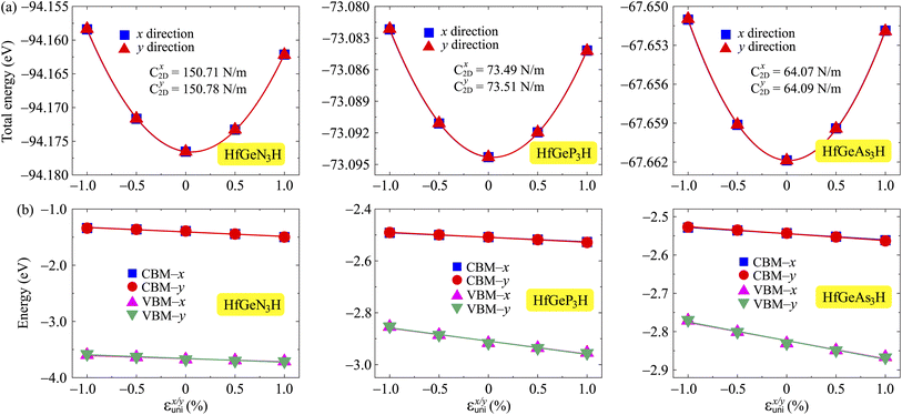
It is demonstrated that the effective masses of electrons in HfGeP3H and HfGeAs3H monolayers are small, indicating that they exhibit high electron mobility. The effective mass of electrons along the x direction  is found to be 0.23m0 (m0 is the free electron mass) for both HfGeP3H and HfGeAs3H monolayers. Meanwhile, the values of
  and
and  for HfGeN3H are calculated to be 2.49m0 and 1.38m0, respectively. This is because the radius of curvature of dispersion around the CBM of HfGeN3H is larger than that of HfGeP3H and HfGeAs3H. The larger the radius of curvature (the flatter the dispersion), the larger the effective mass because the effective mass is inversely proportional to ∂2E(k)/∂k2 as written in eqn (9). Fig. 7 shows the uniaxial strain-dependence of the total energy and band-edge positions in HfGeZ3H monolayers. From Fig. 7, we can see that both C2D and El exhibit quite directionally isotropic along the two transport axes. The calculated results for the transport parameters, including carrier mobilities, of HfGeZ3H monolayers are tabulated in Table 4. Our results reveal that the electron and hole mobilities exhibit directional anisotropy because the values of μe and μh are different along the x and y directions. This is mainly due to the directional anisotropy of effective mass as mentioned above. As revealed in Table 4, HfGeZ3H monolayers exhibit low hole mobility, ranging from 17.69 to 97.35 cm2 V−1 s−1. Meanwhile, due to the low electron effective mass, both HfGeP3H and HfGeAs3H have ultra-high electron mobility, up to 6.40 × 103 cm2 V−1 s−1. This suggests that HfGeP3H and HfGeAs3H monolayers are excellent candidates for applications in electronic devices due to their high electron mobility.
 |
| | Fig. 7 (a) The total energy shifting and (b) positions of the CBM/VBM in HfGeZ3H monolayers as functions of the uniaxial strain εunix/y. | |
Table 4 Computed effective mass of carriers m* (in units of mass of a free electron m0), 2D elastic modulus C2D (N m−1), DP constant El (eV), and mobility of carriers μ (cm2 V −1 s−1) of HfGeZ3H along the x/y transport directions
|
|

|

|
C
2D
x
|
C
2D
y
|
E
l
x
|
E
l
y
|
μ
x
|
μ
y
|
| Electron |
HfGeN3H |
2.49 |
1.38 |
150.71 |
150.78 |
−8.09 |
−7.96 |
10.65 |
19.84 |
| HfGeP3H |
0.23 |
0.53 |
73.49 |
73.51 |
−1.77 |
−1.90 |
6.26 × 10³ |
2.35 × 10³ |
| HfGeAs3H |
0.23 |
0.53 |
64.07 |
64.09 |
−1.64 |
−1.80 |
6.40 × 10³ |
2.31 × 10³ |
| Hole |
HfGeN3H |
1.48 |
2.26 |
150.71 |
150.78 |
−5.69 |
−6.62 |
36.77 |
17.69 |
| HfGeP3H |
0.82 |
0.90 |
73.49 |
73.51 |
−5.01 |
−5.12 |
89.07 |
76.92 |
| HfGeAs3H |
0.77 |
0.83 |
64.09 |
64.09 |
−4.76 |
−4.87 |
97.35 |
86.88 |
4 Conclusive remarks
The structural stabilities and basic physical properties of 2D Janus HfGeZ3H (Z = N, P, As) monolayers were theoretically studied based on the first-principles method. Janus HfGeZ3H monolayers are predicted to be energetically, dynamically, and mechanically stable. Our first-principles simulations demonstrated that HfGeZ3H monolayers are all semiconductors with high electron mobilities up to 6.40 × 103 cm2 V−1 s−1. The influences of the SOC on the band diagrams of HfGeZ3H are significant; in particular, a spin-splitting energy of up to 0.36 eV has been observed in Janus HfGeAs3H monolayers. Besides the in-plane piezoelectric effect, vertical polarization due to the symmetry breaking in Janus HfGeZ3H gives rise to out-of-plane piezoelectric responses with d31 ranging from 0.01 to 0.09 pm V−1. Janus HfGeZ3H monolayers can be proposed for various applications due to their versatile electronic features, high electron mobility, and strong piezoelectric response.
Data availability
All data that support the findings of this study are included within the article.
Conflicts of interest
There are no conflicts of interest to declare.
Acknowledgements
This work was supported by Hue University under project number DHH2023-04-207.
References
- X. Wang, J. Zhou, J. Song, J. Liu, N. Xu and Z. L. Wang, Nano Lett., 2006, 6, 2768–2772 CrossRef CAS PubMed.
- M. Lanza, M. Reguant, G. Zou, P. Lv, H. Li, R. Chin, H. Liang, D. Yu, Y. Zhang, Z. Liu and H. Duan, Adv. Mater. Interfaces, 2014, 1, 1300101 CrossRef.
- M. Yuan, L. Cheng, Q. Xu, W. Wu, S. Bai, L. Gu, Z. Wang, J. Lu, H. Li, Y. Qin, T. Jing and Z. L. Wang, Adv. Mater., 2014, 26, 7432–7437 CrossRef CAS PubMed.
- J. Xin, Y. Zheng and E. Shi, Appl. Phys. Lett., 2007, 91, 112902 CrossRef.
- M. N. Blonsky, H. L. Zhuang, A. K. Singh and R. G. Hennig, ACS Nano, 2015, 9, 9885–9891 CrossRef CAS PubMed.
- K.-A. N. Duerloo, M. T. Ong and E. J. Reed, J. Phys. Chem. Lett., 2012, 3, 2871–2876 CrossRef CAS.
- A.-Y. Lu, H. Zhu, J. Xiao, C.-P. Chuu, Y. Han, M.-H. Chiu, C.-C. Cheng, C.-W. Yang, K.-H. Wei, Y. Yang, Y. Wang, D. Sokaras, D. Nordlund, P. Yang, D. A. Muller, M.-Y. Chou, X. Zhang and L.-J. Li, Nat. Nanotechnol., 2017, 12, 744 CrossRef CAS.
- J. Zhang, S. Jia, I. Kholmanov, L. Dong, D. Er, W. Chen, H. Guo, Z. Jin, V. B. Shenoy, L. Shi and J. Lou, ACS Nano, 2017, 11, 8192–8198 CrossRef CAS PubMed.
- Y. Zhu, Z. Qu, J. Zhang, X. Wang, S. Jiang, Z. Xu, F. Yang, Z. Wu and Y. Dai, Phys. Chem. Chem. Phys., 2024, 26, 4555–4563 RSC.
- T. V. Vu, V. T. T. Vi, H. V. Phuc, A. I. Kartamyshev and N. N. Hieu, Phys. Rev. B, 2021, 104, 115410 CrossRef CAS.
- N. N. Hieu, H. V. Phuc, A. I. Kartamyshev and T. V. Vu, Phys. Rev. B, 2022, 105, 075402 CrossRef CAS.
- T. Zhang, Y. Liang, H. Guo, H. Fan and X. Tian, Appl. Surf. Sci., 2022, 579, 152017 CrossRef CAS.
- N. Ghobadi, S. Gholami Rudi and S. Soleimani-Amiri, Phys. Rev. B, 2023, 107, 075443 CrossRef CAS.
- N. T. Hiep, C. Q. Nguyen and N. N. Hieu, Appl. Phys. Lett., 2023, 123, 092102 CrossRef CAS.
- D. Bezzerga, E.-A. Haidar, C. Stampfl, A. Mir and M. Sahnoun, Nanoscale Adv., 2023, 5, 1425–1432 RSC.
- T. V. Vu, H. V. Phuc, A. I. Kartamyshev and N. N. Hieu, Appl. Phys. Lett., 2023, 122, 061601 CrossRef CAS.
- Y. Zhang, Y. Shen, J. Liu, L. Lv, M. Zhou, X. Yang, X. Meng, B. Zhang and Z. Zhou, Phys. Chem. Chem. Phys., 2023, 25, 22889–22899 RSC.
- B. Akgenc, E. Vatansever and F. Ersan, Phys. Rev. Mater., 2021, 5, 083403 CrossRef CAS.
- D. H. Ozbey, M. E. Kilic and E. Durgun, Phys. Rev. Appl., 2022, 17, 034043 CrossRef CAS.
- B. Akgenc, Comput. Mater. Sci., 2020, 171, 109231 CrossRef CAS.
- A. Kaur, S. Sharma, P. Nandi and A. De Sarkar, Phys. E, 2023, 154, 115791 CrossRef CAS.
- N. Tripathy and A. De Sarkar, J. Phys.: Condens.Matter, 2023, 35, 335301 CrossRef PubMed.
- H.-N. Zhang, Y. Wu, C. Yang, L.-H. Zhu and X.-C. Wang, Phys. Rev. B, 2021, 104, 235437 CrossRef CAS.
- Y.-Q. Li, X.-Y. Wang, S.-Y. Zhu, D.-S. Tang, Q.-W. He and X.-C. Wang, J. Phys. Chem. Lett., 2022, 13, 9654–9663 CrossRef CAS PubMed.
- H. Zhu, Y. Wang, J. Xiao, M. Liu, S. Xiong, Z. J. Wong, Z. Ye, Y. Ye, X. Yin and X. Zhang, Nat. Nanotechnol., 2014, 10, 151–155 CrossRef PubMed.
- W. Wu, L. Wang, Y. Li, F. Zhang, L. Lin, S. Niu, D. Chenet, X. Zhang, Y. Hao, T. F. Heinz, J. Hone and Z. L. Wang, Nature, 2014, 514, 470–474 CrossRef CAS PubMed.
- R. Fei, W. Li, J. Li and L. Yang, Appl. Phys. Lett., 2015, 107, 173104 CrossRef.
- Y. Guo, S. Zhou, Y. Bai and J. Zhao, Appl. Phys. Lett., 2017, 110, 163102 CrossRef.
- T. V. Vu, H. V. Phuc, A. I. Kartamyshev and N. N. Hieu, Appl. Phys. Lett., 2023, 122, 061601 CrossRef CAS.
- T. V. Vu, B. D. Hoi, A. I. Kartamyshev and N. N. Hieu, J. Appl. Phys., 2024, 135, 074301 CrossRef CAS.
- Y.-L. Hong, Z. Liu, L. Wang, T. Zhou, W. Ma, C. Xu, S. Feng, L. Chen, M.-L. Chen, D.-M. Sun, X.-Q. Chen, H.-M. Cheng and W. Ren, Science, 2020, 369, 670–674 CrossRef CAS PubMed.
- L. Wang, Y. Shi, M. Liu, A. Zhang, Y.-L. Hong, R. Li, Q. Gao, M. Chen, W. Ren, H.-M. Cheng, Y. Li and X.-Q. Chen, Nat. Commun., 2021, 12, 2361 CrossRef CAS PubMed.
- R. Sibatov, R. Meftakhutdinov and A. Kochaev, Appl. Surf. Sci., 2022, 585, 152465 CrossRef CAS.
- N. T. Hiep, N. P. Q. Anh, H. V. Phuc, C. Q. Nguyen, N. N. Hieu and V. T. T. Vi, Phys. Chem. Chem. Phys., 2023, 25, 8779–8788 RSC.
- H. T. Nguyen, N. Q. Cuong, V. T. T. Vi, N. N. Hieu and L. P. T. Tran, Phys. Chem. Chem. Phys., 2023, 25, 21468–21478 RSC.
- N. P. Q. Anh, N. T. Hiep, D. V. Lu, C. Q. Nguyen, N. N. Hieu and V. T. T. Vi, Nanoscale Adv., 2023, 5, 6705–6713 RSC.
- T. V. Vu, H. V. Phuc, C. V. Nguyen, V. T. T. Vi, A. I. Kartamyshev and N. N. Hieu, Phys. Chem. Chem. Phys., 2022, 24, 16512–16521 RSC.
- G. Kresse and J. Furthmüller, Phys. Rev. B: Condens. Matter Mater. Phys., 1996, 54, 11169–11186 CrossRef CAS PubMed.
- G. Kresse and J. Furthmüller, Comput. Mater. Sci., 1996, 6, 15–50 CrossRef CAS.
- P. E. Blöchl, Phys. Rev. B: Condens. Matter Mater. Phys., 1994, 50, 17953 CrossRef PubMed.
- G. Kresse and D. Joubert, Phys. Rev. B: Condens. Matter Mater. Phys., 1999, 59, 1758–1775 CrossRef CAS.
- J. P. Perdew, K. Burke and M. Ernzerhof, Phys. Rev. Lett., 1996, 77, 3865 CrossRef CAS PubMed.
- J. Heyd, G. E. Scuseria and M. Ernzerhof, J. Chem. Phys., 2003, 118, 8207 CrossRef CAS.
- S. Grimme, J. Antony, S. Ehrlich and H. Krieg, J. Chem. Phys., 2010, 132, 154104 CrossRef PubMed.
- A. H. MacDonald, W. E. Picket and D. D. Koelling, J. Phys. C: Solid State Phys., 1980, 13, 2675 CrossRef CAS.
- A. Togo, L. Chaput and I. Tanaka, Phys. Rev. B: Condens. Matter Mater. Phys., 2015, 91, 094306 CrossRef.
- J. Bardeen and W. Shockley, Phys. Rev., 1950, 80, 72 CrossRef CAS.
- J. P. Perdew and M. Levy, Phys. Rev. Lett., 1983, 51, 1884–1887 CrossRef CAS.
- L. Hedin, Phys. Rev., 1965, 139, A796 CrossRef.
- M. Born and K. Huang, Am. J. Physiol., 1955, 23, 474 CrossRef.
- R. C. Andrew, R. E. Mapasha, A. M. Ukpong and N. Chetty, Phys. Rev. B: Condens. Matter Mater. Phys., 2012, 85, 125428 CrossRef.
- X. Cai, G. Chen, R. Li, W. Yu, X. Yang and Y. Jia, Phys. Chem. Chem. Phys., 2023, 25, 29594–29602 RSC.
- C. Lee, X. Wei, J. W. Kysar and J. Hone, Science, 2008, 321, 385–388 CrossRef CAS PubMed.
- R. D. King-Smith and D. Vanderbilt, Phys. Rev. B: Condens. Matter Mater. Phys., 1993, 47, 1651–1654 CrossRef CAS PubMed.
- X. Cai, G. Chen, R. Li, Z. Pan and Y. Jia, J. Mater. Chem. C, 2024, 12, 4682 RSC.
- T. V. Vu, B. D. Hoi, A. I. Kartamyshev and N. N. Hieu, J. Appl. Phys., 2024, 135, 074301 CrossRef CAS.
- S.-D. Guo, W.-Q. Mu, Y.-T. Zhu, R.-Y. Han and W.-C. Ren, J. Mater. Chem. C, 2021, 9, 2464–2473 RSC.
|
| This journal is © The Royal Society of Chemistry 2024 |
Click here to see how this site uses Cookies. View our privacy policy here.  Open Access Article
 ab,
Huynh V.
Phuc
 *c,
Le T. T.
Phuong
 d,
Vo T. T.
Vi
 e,
A. I.
Kartamyshev
ab and
Nguyen N.
Hieu
 *fg
*fg


 . The temperature is marked by T. C2D denotes the elastic modulus and El refers to the DP constant. The rectangular supercell is chosen to calculate the carrier mobilities of the studied structures with T = 300 K.


 is found to be 0.23m0 (m0 is the free electron mass) for both HfGeP3H and HfGeAs3H monolayers. Meanwhile, the values of
  and
and  for HfGeN3H are calculated to be 2.49m0 and 1.38m0, respectively. This is because the radius of curvature of dispersion around the CBM of HfGeN3H is larger than that of HfGeP3H and HfGeAs3H. The larger the radius of curvature (the flatter the dispersion), the larger the effective mass because the effective mass is inversely proportional to ∂2E(k)/∂k2 as written in eqn (9). Fig. 7 shows the uniaxial strain-dependence of the total energy and band-edge positions in HfGeZ3H monolayers. From Fig. 7, we can see that both C2D and El exhibit quite directionally isotropic along the two transport axes. The calculated results for the transport parameters, including carrier mobilities, of HfGeZ3H monolayers are tabulated in Table 4. Our results reveal that the electron and hole mobilities exhibit directional anisotropy because the values of μe and μh are different along the x and y directions. This is mainly due to the directional anisotropy of effective mass as mentioned above. As revealed in Table 4, HfGeZ3H monolayers exhibit low hole mobility, ranging from 17.69 to 97.35 cm2 V−1 s−1. Meanwhile, due to the low electron effective mass, both HfGeP3H and HfGeAs3H have ultra-high electron mobility, up to 6.40 × 103 cm2 V−1 s−1. This suggests that HfGeP3H and HfGeAs3H monolayers are excellent candidates for applications in electronic devices due to their high electron mobility.