 Open Access Article
3D nanoplasmonic structure for ultrahigh enhanced SERS with less variability, polarization independence, and multimodal sensing applied to picric acid detection†
Anand M.
Shrivastav‡
 ab,
Mohammad
Abutoama‡
 acd and
Ibrahim
Abdulhalim
 *a
*a
aDepartment of Electro-Optics and Photonics Engineering, School of Electrical and Computer Engineering and The Ilse-Katz Institute for Nano-scale Science and Technology, Ben Gurion University, Beer Sheva, 84105, Israel. E-mail: abdulhlm@bgu.ac.il
bDepartment of Physics and Nanotechnology, College of Engineering and Technology, SRM Institute of Science and Technology, Kattankulathur, Chennai, Tamil Nadu 603203, India. E-mail: anandmos@srmist.edu.in
cDTU Electro, Technical University of Denmark, Ørsteds Plads, Building 343, 2800 Kgs, Lyngby, Denmark. E-mail: moabo@fotonik.dtu.dk
dNanoPhoton – Center for Nanonphotonics, Ørsteds Plads, Building 345A, 2800 Kgs, Lyngby, Denmark
First published on 18th September 2024
Abstract
Surface-enhanced Raman scattering (SERS) is recognized as a powerful analytical method. However, its efficacy is hindered by considerable signal variability stemming from factors like surface irregularities, temporal instability of the substrate, interference with substrate signal, polarization sensitivity and uneven molecular distribution. To address these challenges, a new strategy is employed to enhance the reproducibility of SERS signals. Initially, a periodic 3D metallic structure is utilized to achieve polarization-independent ultrahigh enhancement. Additionally, signal averaging over multiple points and normalization are implemented. The integration of these techniques enables multimodal sensing (SERS, SEF, SPR) using a plasmonic chip, demonstrating ultrahigh enhancement through the interaction of extended and localized plasmons alongside nanoantenna-type resonances. The chip comprises a periodic silver 2D grating adorned with Au nanocubes, behaving as a 3D metasurface to amplify plasmonic local fields, thus facilitating SERS. Its uniformity and polarization independence together with signal averaging and normalization mitigate signal variability. Fabricated via electron beam lithography, the chip's performance is evaluated for surface-enhanced fluorescence (SEF) and SERS using Rhodamine 6G as the target molecule. Results exhibit two orders of magnitude enhancement factor for SEF and 2.5 × 10⁷ for SERS. For chemical sensing, the chip is tested for picric acid detection across a concentration range from nanomolar to millimolar, demonstrating a detection limit of approximately 3 nM.
1. Introduction
Raman Spectroscopy has demonstrated its potency as a formidable tool for molecular fingerprint analysis, with diverse applications across fields such as security, pharmaceuticals, biomedical research, and agriculture. Nevertheless, its efficacy is curtailed by weak inelastic scattering, resulting in the generation of only one Raman-scattered photon for every 107 incident photons. This limitation constrains its broader applicability,1–3 which can be improved by enhancing the intensity of Raman signals in what is called surface enhanced Raman scattering (SERS). Traditionally, SERS is accomplished when the target material is situated in a highly localized manner over a rough plasmonic nanostructured surface, with the corresponding plasmonic resonance wavelength overlapping both the laser excitation wavelength and the vibrational Stokes regime.4–6 Extensive efforts have been undertaken to design and create innovative SERS substrates, yielding high levels of enhancement factors ranging typically from 103 to 1010. Typically, the enhancement factor in a SERS substrate is attributed to two primary components: electromagnetic enhancement and chemical enhancement. The electromagnetic enhancement arises from the heightened localized optical field resulting from the presence of plasmonic nanomaterial near the Raman-active molecule, leading to a remarkable improvement in the SERS signal.7,8 However, this enhancement strongly relies on various parameters, including the material, shape, and structure of the plasmonic nanomaterial, as well as the surrounding environment. The second major component is chemical enhancement, involving a charge transfer mechanism between the plasmonic surface and the Raman molecule. This process induces a change in molecular polarizability, resulting in a significantly enhanced Raman signal, often reaching orders of magnitude higher.9,10 Harnessing the substantial electromagnetic enhancement, coupled with molecular fingerprint technology and advanced nanofabrication techniques, SERS-based sensors represent a rapidly advancing research domain, emerging as a predominant method for biosensing applications, even down to the level of single molecules.11,12To date, a wide range of SERS substrates have been reported that achieve high local field enhancements including Au nanoparticles,13 Au nanorings,14 Au nonorods,15,16 Au nanodimers,17 Ag nano sculptured thin films,18–20 Ag nanoclusters,21 and many others. To further enhance the SERS intensity the coupling between localised and extended plasmon configurations was proposed and found very efficient.4,22–24 The ESP (extended surface plasmons) causes some local field enhancement factor Fesp, it excites the LSP (localized surface plasmons) which has enhancement factor of Flsp, however the final field enhancement factor was found to be even larger than the simple multiplication of the two enhancement factors FespFlsp. All these structures have demonstrated enhancement factors of up to the orders of 105–1010. Nevertheless, although these structures offer substantial enhancement factors, they still pose limitations for industrial applications due to notable variability in the SERS signal across the substrate area. This variability stems from factors like surface irregularities, uneven molecular adsorption on the surface, fluctuations in laser light, and polarization dependence, temporal instability of the substrate25–27 and interference with substrate signal28etc. To overcome these challenges, we have developed a polarization-independent two-dimensional subwavelength periodic metallic 3D structure composed of silver boxes decorated with gold nanocubes as a SERS substrate, ensuring both low variability and high local field enhancement due to effective ESP–LSP interaction. We noticed the excitation of nanoantenna type resonances on top of the silver boxes when the ESP is excited as their lateral dimensions are larger than the extended plasmon wavelength.
The primary rationale for choosing metallic gratings lies in their uniformity across a substantial surface area, contrasting with nanostructures that may be grown or deposited on a surface. This uniformity plays a crucial role in minimizing signal variability for SERS. Additionally, the planar nature of metallic gratings presents the added benefit of requiring minimal optical components, such as prisms or optical fibers, for plasmonic excitations.4,23,24 It is important to note that the designed metallic gratings have a period smaller than the wavelength of the incident light, which prevents diffraction and ensures that the obtained spectra are solely due to the contribution of optical resonant excitations.29 These types of gratings are referred to as subwavelength gratings, and fall under the category of plasmonic metasurfaces. In our previous work, we designed one-dimensional subwavelength metallic gratings and demonstrated their application in refractive index sensing, as well as in SERS and surface-enhanced fluorescence (SEF) based applications using the same substrate.30 Additionally, several subwavelength grating configurations can be used to excite various resonance phenomena. Examples include: (a) designing the grating over a thin metallic film to achieve resonance excitation of ESPs and cavity modes,31 (b) using a thin dielectric grating over a metallic thin film to provide ESP excitation and guided mode resonance (GMR),32–34 (c) employing metallic thin nano slits on a dielectric substrate for enhanced optical transmission (EOT),35–37 and (d) utilizing thin dielectric gratings with or without a waveguide layer to exhibit GMR.38–40 Furthermore, as mentioned 2D grating can give ultrahigh enhancement of SERS through the ESP–LSP coupling23 basically achieved through decorating plasmonic nanostructures over the ESP supported platform, which can be grating or metallic thin film. For SERS applications, 1D metallic gratings are particularly useful for SERS, however, they still face limitations due to variability issues, as mentioned in the previous paragraph, which stems from factors such as surface uniformity, and polarization dependence.
In this research, we present a novel approach to mitigate variability arising from nonuniformity and light polarization by designing two-dimensional silver gratings decorated with gold nanocubes for ultrahigh SERS enhancement. These gratings are specifically crafted to overlap optical resonances corresponding to both TE (transverse electric) and TM (transverse magnetic) polarizations. The selection of gold nano-cubes as the structure that supports LSPs is motivated by their eight-cornered configuration, generating a higher concentration of enhanced field hot-spots across the sensor surface. The final proposed substrate is fabricated using the e-beam lithography method and characterized through reflectance spectrum analysis. Subsequently, the grating chip undergoes characterization using surface-enhanced fluorescence (SEF) and surface-enhanced Raman spectroscopy (SERS) methods, employing Rhodamine 6G molecules adsorbed on the chip surface, thus demonstrating its use for multimodal sensing. Finally, the substrate is applied to explosive detection, with picric acid (PA) as the targeted sensing material.
2. Numerical simulations and chip design
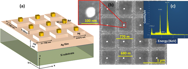
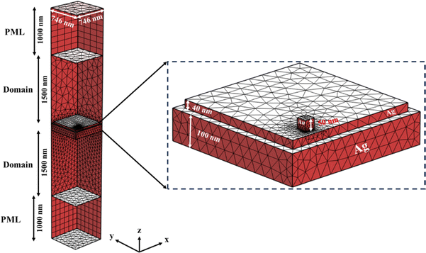
The two-dimensional metallic grating was meticulously designed using COMSOL Multiphysics, involving multiple iterations. The finalized design of the 3D plasmonic structure is illustrated in Fig. 1(a). The thickness (d) of the continuous metal film below the 2D grating is set at 100 nm to avoid transmission into the silicon substrate and to operate in reflection mode. The 2D grating has a period (Λ) of 746 nm, line width (w) of 671 nm, and grating height (h) of 40 nm. All these parameters underwent optimization through the numerical study conducted in COMSOL. The optimization was basically performed to have the main resonance at ∼785 nm (the 1st order of the extended surface plasmon mode) to match with the wavelength of the laser to be used for the Raman measurements. Furthermore, Au nano-cubes (50 nm × 50 nm × 50 nm) were introduced onto the grating's surface to facilitate the interactions of extended and localized plasmons, resulting in a heightened local electromagnetic field at the hot spots. This strategic addition enhances the overall performance of the chip.22,23 Although the chip is designed to have the nanocubes centered on the Ag boxes, due to fabrication limitations, the obtained chip has off-centered gold nanostructures along with partial changes in the numbers, as shown in the SEM image below (Fig. 1(b)). The off-diagonal shift was found not to affect the performance, which can be seen in Fig. S1† where the resonances are obtained at 791 nm for off-diagonal and 785 nm centered Au nanocubes respectively. The fabrication process of the chip will be discussed in the experimental section of the manuscript. Hence, to obtain realistic results, the calculations are repeated keeping all the real parameters found in the fabricated ones like for electric field calculations, the size of Au boxes is chosen as (60 nm × 60 nm × 60 nm). Additionally, Fig. 1(c) represents the EDX spectroscopic data for the fabricated substrate which has been further discussed in the experimental section.The field distribution pattern in x–z and x–y planes was calculated using COMSOL Multiphysics, which is based on the finite element analysis (FEA) method. The incident light beam is modeled as a plane wave propagating along the z-axis coming from the air domain (see Fig. 2). Perfectly Matched Layer (PML) boundary condition is imposed for z-coordinate above and below the superstrate (air) and substrate (Si) domains. Field monitor is used at a fixed z position above the nanostructure to detect the beam reflection as a function of incidence wavelength. Adaptive mesh is used over the different domains to achieve reliable calculations. Normal incident light is used in all the simulations. The dielectric functions of the materials used in the simulations were interpolated based on the data taken from the Sopra database (http://sspectra.com/).
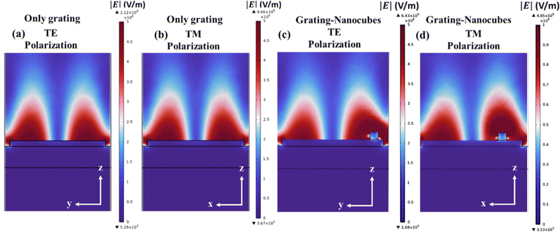
Fig. 3(a) and (b) depicts the electric field amplitude for the proposed grating structure corresponding to TE and TM polarized light respectively without the Au nanocubes. From the figure, the almost similar electric field amplitude is obtained for both the polarizations providing the opportunity to minimize the polarization dependence for SERS. In addition, Fig. 3(c) and (d) corresponds to the electric field intensities for the structures having Au nanocubes on the top of grating. An improvement by factor ×6 is obtained as seen in Fig. 3 where maximum electric field is compared with/without Au nanocubes over the Ag grating. This is because of the coupling of extended surface plasmons (ESPs, due to the grating) with localized surface plasmons (LSPs, due to plasmonic nanocubes) providing the higher enhancement in the local field, compared to the bare grating structure. Here, the simulations done on the fabricated structure with the nanocubes off centred. Note that when the ESP is excited two maxima of the local field appear on the surfaces of the Ag boxes which have lateral dimension of 671 nm. When the ESP is excited by the periodic structure it propagates, hits the edges of the Ag box and partially reflects back. As a result, a standing wave is formed, which is a nanoantenna type resonance causing enhanced localization of the field at the hot spots. Note also that the off centring of the nanocubes causes a difference between the TE and TM field distribution (Fig. 3(c) and (d)) which can be understood due to symmetry breaking. It may also be noted that 2D designed grating plays an important role as it eliminates the effect of the polarization of input light on the orientation of the substrate. A similar study was reported by Xiao et al. in 2018 to obtain polarization independence. However, in their works the 2D sinusoidal grating was prepared by using two-beam interference fabrication process and they have successfully demonstrated the polarization independent nature of the grating structure.41 In the similar manner, if one refers to Fig. 3(c) and (d), for the incident TE and TM polarization of the input light, a nearly similar electromagnetic behaviour is obtained, however in the case of 1D grating one can simply observe the effect of polarization as the extended plasmons can be excited only with TM polarization (along the grating vector). When the structure is polarization sensitive then any small changes of the structure manifest in large changes in the signal, for example due to polarization change on the surface. Also, when a polarizer is used then polarization instabilities might affect the variability of the signal.
3. Experimental analysis
3.1. Materials
Rodhamine 6G and picric acid (PA) were procured from Sigma-Aldrich Pvt. Ltd. Ethanol (99.9% pure) was obtained from ROMICAL chemicals Ltd, Israel. The chip was fabricated at nanofabrication facility at BGU, with 99% purity of gold (Au) and silver (Ag). All the materials were used in the similar form as received from the vendor, without any further modifications.3.2. Chip fabrication and characterizations
The proposed chip underwent fabrication at the BGU nanofabrication center utilizing electron beam lithography. Initially, a 100 nm thick silver film was deposited on the Si wafer, followed by the thin film deposition of photoresist. Subsequently, based on the defined structure (as illustrated in Fig. 1(a)), the photoresist was hardened only in regions where the presence of Ag was unnecessary for grating fabrication, covering the entire surface. Consequently, the photoresist was confined to areas of Ag in the grating surface. Next, a 40 nm thick Ag film was deposited across the entire surface, followed by surface cleaning to eliminate the hardened photoresist. This selective process resulted in Ag deposition exclusively in the line width part of the grating, completing the 2D grating fabrication. The same procedure was then repeated for the Au nanocubes over the grating surface. As displayed in Fig. 1(b) the scanning electron microscope (SEM) image of the fabricated chip, showcasing a high degree of uniformity along the surface. The bright spot on the surface corresponds to Au nanocubes. Some variation in the fabricated sensing chip occurred compared to the proposed design, attributed to experimental limitations. Specifically, the nanocubes were obtained off-centered and the decentring slightly varied across the surface. Although from the SEM image we could not confirm precisely that prepared Au nanocubes are in cubical shapes as the light get saturated at higher beam intensity and limited resolution of the instrument. For the elemental analysis of the fabricated chip, we have also performed the EDX spectroscopy providing the confirmation of Ag and Au on the surface as shown in Fig. 1(c). The elemental data corresponding to chip fabrication is given in Table 1. It may be noted carbon peak is obtained in EDX due the photoresist remnants used in the fabrication process.| Material | wt% | Error % |
|---|---|---|
| Ag (silver) | 87.5 | 0.9 |
| Si (silicon) | 9.2 | 0.4 |
| Carbon (C) | 2.6 | 0.5 |
| Gold (Au) | 0.7 | 0.2 |
3.3. Reflectance measurements
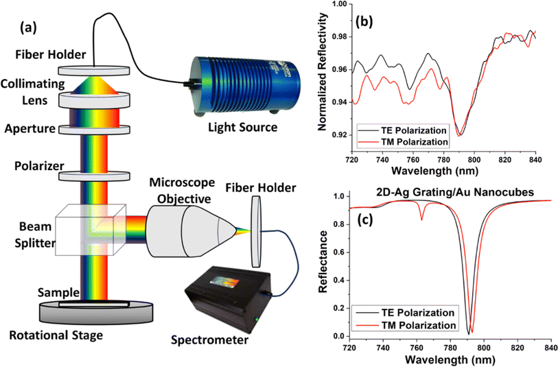
After the chip fabrication, the reflectance measurements were taken using a broadband source and a spectrometer using the setup shown in Fig. 4(a). The white light was incident normally to the substrate and corresponding reflected beam was transferred to a spectrometer using beam splitter. The polarization of input light can also be tuned using the rotatable polarizer after the collimation of the input light. Fig. 4(b) represents the output reflected spectra for both TE and TM polarized light, depicting that the ESP resonance is obtained at around 785 nm wavelength for both the polarizations. It should be noted that this wavelength is very important since it overlaps with the laser wavelength used for the Raman excitation, in agreement with the design (Fig. 4(c)). This confirms the polarization independent response of the designed chip. Although, there is a small dip obtained at 762 nm for TM polarized light but to obtain the polarization independent nature in SERS, one needs to focus on the resonance near the laser wavelength (785 nm), where for the two polarizations a similar resonance is obtained. The change in depth of the experimental resonance dips is due to the losses and as well as experimental/fabrication limitations such as the use of etching which causes some roughness, well known to affect strongly surface plasmons. The roughness can be seen in the SEM image.3.4. Surface enhanced fluorescence (SEF) characterisations
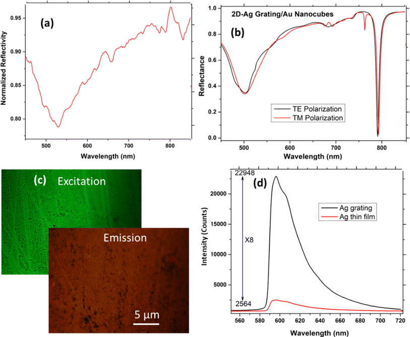
While measuring the reflectance spectra for the fabricated chip, shown in Fig. 5(a), it was found that the chip possesses one more resonance dip around 500–520 nm. Using the SPR excitation formulae from gratings possible to verify that it is indeed a 2nd order SPR resonance: | (1) |
Since, one of the resonances obtained falls within the excitation fluorescence window of Rhodamine 6G (R6G), it was used as a fluorescence tag molecule by spin coating of 1 mg ml−1 R6G over the fabricated chip surface. Fluorescence measurements were taken using Olympus fluorescence microscope with an Hg arc-lamp as excitation light. The green Hg line at 546 nm was used for excitation and the emission was detected using a red filter at 590 nm. The detection was done using a high sensitivity cooled CCD camera with a controlled exposure time. Fig. 5(b) represents the theoretical reflection results of the proposed chip claiming the similar nature of both TE and TM polarized light. Fig. 5(c) shows the excitation and emission images of the chip surface. To evaluate the enhanced SEF, the fiber coupled spectrometer was added to one of the eyepiece channels of the fluorescence microscope to obtain the fluorescence spectrum. Two different kinds of chips were placed under the microscope including the fabricated 3D plasmonic chip along with the bare Ag coated chip with R6G. For more quantitative evaluation the corresponding fluorescence counts were collected by a spectrometer connected to the microscope in a conjugate plane to the camera.42Fig. 5(d) shows around an 8 times enhanced excitation using the 3D chip compared to bare Ag coated chip and the main reason is the high localized field near the 2D grating surface. As it is known that the flat Ag surface also enhances the fluorescence by about factor ×10, hence possible to conclude that the overall SEF enhancement of the chip is close to ×80. Considering the fact that the SPR is at 504 nm, and the excitation is at 546 nm, even higher SEF enhancement factor is expected when they coincide. It can be noted that the un-smoothness and irregularity in the chip surface are partially due to the etching during the fabrication process and partially due to the ununiform immobilization of R6G molecules. The immobilization is done through the drop casting method by dropping 1 mg ml−1 solution of R6G. Because of this, at some places the clusters of R6G are formed providing irregular surface. However, it can easily be removed by soft sonicating in ethanol ensuring reproducibility of the substrate. Irregularities of R6G can affect the variability over the surface but the irregularities due to the fabrication process are random and are believed not to affect it much such the measurement if from an area of many periods.
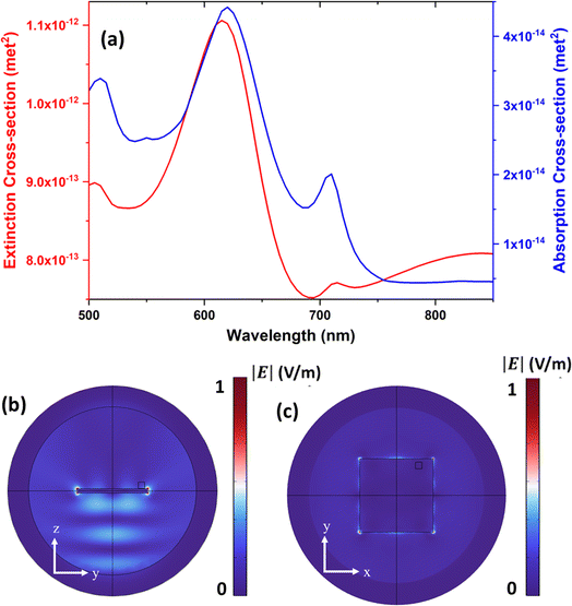
To further elucidate the origin of the different resonances and the observed signals enhancement, the extinction and absorption cross-section of the fabricated structure were calculated as shown in Fig. 6(a) providing a broad spectrum around 550–650 nm. It also justifies the enhanced fluorescence when the green laser around 532 nm is used as what observed in Fig. 5(c) and (d) respectively. In addition, the electric field distribution of the structure for two different side slice cross-section and as well as top cross-section is represented in Fig. 6(b) and (c) respectively.
3.5. SERS measurements
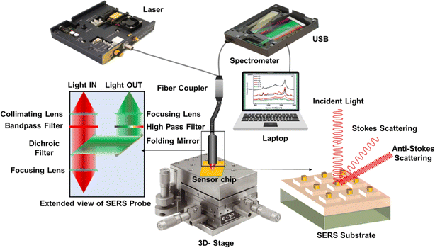
The inset of Fig. 7 provides an expanded view of the SERS probe. The laser light is collimated and passes through a sharp bandpass filter to ensure a single wavelength. Subsequently, it is tightly focused to a 300 μm diameter spot onto the substrate using another convex lens. The same lens is used to capture the reflected and scattered light, which is then directed through a dichroic filter to separate the incident and collected light. The collected light is further transmitted through a long-pass filter to eliminate the Rayleigh scattering, the laser reflected beam, and the anti-Stokes Raman scattered lines. Finally, another lens is employed to focus the Raman scattered light onto the input end of the collecting optical fiber, which is then interfaced with the spectrometer.
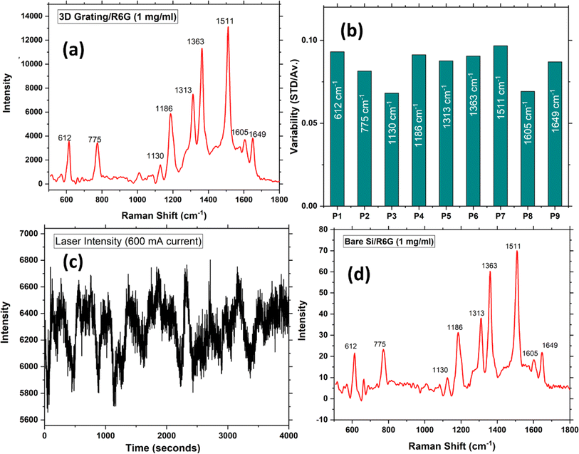
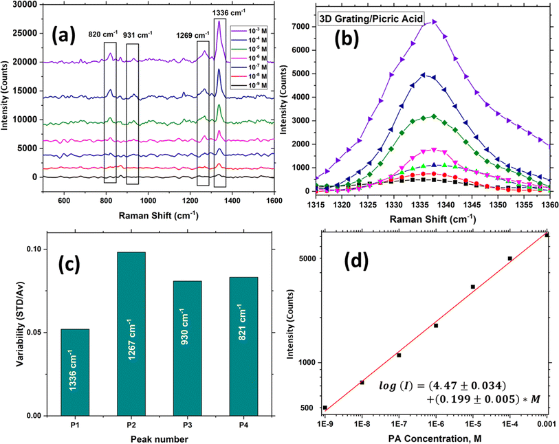
As mentioned, the variability in the Raman signal is a crucial issue limiting the detection limit of sensors based on SERS, which is calculated by taking the ratio between the standard deviation in SERS signal and the average while measuring the SERS spectra at ten different locations. This originates from several factors: laser stability, variability of plasmonic structure, variability of the analyte concentration on the surface. As can be seen from Fig. 8(c) there are two sources of noise in the laser intensity, the low frequency one which is nearly 15% peak-to-peak, and the high frequency one which is around 5% peak-to-peak. Upon averaging the high frequency one can be reduced drastically, however the low frequency one which not completely random cannot be cancelled out completely by averaging, however this its time scale is in minutes, its effect may be minimized by normalization. The SERS signal variability was assessed by recording 10 measurements at different locations on the sensor chip, and the ratio of the standard deviation to the average was plotted for each peak in Fig. 8(b). The figure clearly shows that the variability falls within the range of 0.06–0.1 (or 6–10%). In contrast, in typical cases, the signal variation is usually around 15–30% or even higher.44–46
The improvement in signal reproducibility is attributed to the presence of a homogeneous sensor surface achieved through the use of a 2D grating, which effectively eliminates changes in the enhancement factor and the polarization dependency of the signal, as well as to the normalization of the signal to the average. Another important factor is the variations in the concentration of the analyte molecules on the surface. This can be improved using more sophisticated techniques of depositing the analyte molecules on the surface such as using nano-injectors. Normalization to a constant Raman peak that does not change with the analyte concentration is another approach to minimize the effect of the variations in the analyte concentration.
3.5.2.1 Calculation of enhancement factor. The SERS enhancement factor is a crucial parameter for evaluating the performance of a sensor surface. It is determined by comparing the intensity of the SERS signal obtained from each adsorbed molecule on the surface with the Raman signal intensity of each molecule in the bulk medium, as expressed below:47,48
Here, IRaman and ISERS represent the peak intensities of the Raman measurement under normal and SERS conditions, respectively. Nbulk and Nads refer to the number of R6G molecules in the scattering volume for the normal Raman measurement and SERS measurement, respectively. In our case, the concentration of R6G molecules (conc. 1 mg ml−1) in a 1 μl volume is estimated to be approximately 1.255 × 10¹⁶, considering the molecular weight of R6G as 479.02. Studies have shown that the surface area covered by a single R6G molecule is approximately 1 nm2 (molecular area),49 while the substrate has an area of 1 mm2. This suggests that the maximum number of molecules that can be accommodated within a single layer is approximately 1012. It is important to note that SERS can be observed for molecules within a few tens of nm distance from the surface according to the field distribution observed in Fig. 3, which limits the total number of molecules taking part of SERS to be within a few to ten monolayers of R6G.
Considering laser parameters such as a spot diameter of 0.3 mm and a depth of field of 1 mm, the number of molecules eligible for SERS (NSERS) would be 2.826 × 10¹¹ (considering 10 monolayers), while the number of molecules for Raman scattering (NRaman) would be approximately 3.55 × 10¹⁷, since 1 mg of R6G is required to collect the Raman spectra of bulk sample. To determine the enhancement factor, Raman spectra for bulk samples were recorded (following similar molecular deposition steps on a flat silicon surface) and plotted in Fig. 8(d). Using the numbers mentioned above and the above equation, the total SERS enhancement factor corresponding to each peak was calculated and found to be in the range 2–5 × 10⁷. It is noteworthy that higher enhancement is achieved near the edges of Au nano cubes and the corners of the grating structure, where the molecules are located near the hotspots on the surface. In these areas, the SERS enhancement may be underestimated. Therefore, considering these circumstances, the obtained enhancement factor, with the order of 2.6 × 10⁷, is significantly larger than that on conventional structures falling on the side of the ultrahigh enhancement cases. Further, we would like to mention that the above calculation is an approximation as it is difficult to predict the exact number of molecules on the grating keeping in mind the possibility of nonuniformity along the surface.
3.5.3.1 Calibration, and limit of detection. Fig. 9(d) showcases the calibration curves for PA sensing using the fabricated SERS substrate, with the Raman intensity of the peak at wavenumber 1336 cm−1 serving as the measurement parameter. The figure demonstrates that as the peak concentrations vary from nM to mM, the peak height exhibits a monotonic change, ranging from 495 to 7134 counts. Moreover, the detection limits for both calibration methods are determined using the standard protocol, which involves using the expression: LOD = 3 × (standard deviation/sensitivity near the minimum concentration).
In the present scenario, the sensitivity near a concentration of 1 nM of PA is calculated to be 24.4 counts per nM. The standard deviation is determined to be 24.7 counts (approximately 5% of the counts at 1 nM, as shown in Fig. 9(c)). These values yield a minimum detection limit for the sensor of 3.04 nM. This detection limit is comparable to the best methods for PA sensing utilizing P–Si-based and other SERS substrates, as indicated in Table 2. As one can see from the table below, few studies reported better or comparable LOD values for PA sensing with a higher enhancement factor and a simpler fabrication approach. For example, the works done by Hakonen et al., where hydrophobic Ag nanopillars and handheld Raman spectrometer for PA detection have been demonstrated with ultralow LOD value of 20 ppt.51 In another study reported by our group, we have shown the sub nanomolar LODs of PA using Au coated porous silicon substrates providing 3D plasmonic hot spots.24
| Substrate configuration | PA detection range | Detection limit | Ref. |
|---|---|---|---|
| Fe/ripple nanostructured Au | 10−6–10−4 M | 5 μM | 52 |
| Paper-based substrate/Au nanoparticles & nanostars | 5–50 μM | 5 μM | 53 |
| Porous Si (P–Si)/Ag nanoparticles | 0–100 μM | 2 μM | 54 |
| Filter paper/Au nanotriangle | 10−6–10−4 M | 10−6 M | 55 |
| Hydrophobic Ag nanopillar | 0–20 ppb | 20 ppt | 51 |
| P–Si photonic crystals/Ag Nanoparticles | 10−7–10−4 M | 0.1 nM | 56 |
| P–Si photonic crystals/Au Nanoparticles | 10−9–10−5 M | 1 nM | 57 |
| P–Si/Ag– Au alloys | 10−7–10−3 M | 36 nM | 58 |
| Micro P–Si/Au thin film | 10−9–10−3 M | 7.48 nM, (based on peak height) | 24 |
| 2.87 nM, (based on peak ratio) | |||
| Hydrophobic Ag nanopillars | 0–87 pM (0–20 ppb) | 87.2 fM (20 ppt) | 51 |
| 2D Ag grating/Au nanocubes | 10−9–10−3 M | 3.04 nM | Present work |
It is worth noting that price is also one of the important aspects while designing SERS substrates. Several studies reported cost-effective and higher electromagnetic enhancements enabling lower detection limits.59–62 However, in our approach, the goal is to design a substrate ensuring high stability through polarization insensitivity using 2D grating. Although we designed the substrate to attain higher electromagnetic enhancement, we also focused on the polarization insensitivity. Indeed, the current technology required higher cost but developments in nanofabrication may also enable to fabricate such substrate with lower costs, in particular in mass production.
Next aspect which plays a very important role in an effective substrate is reproducibility. In our case, three different substrates are prepared. A small deviation in SERS results is obtained for each substrate as strongly dependent on the position of Au nano-cubes on the top of the grating. The results shown in the manuscript belong to the best one matching the simulation. One can clearly say that the reproducibility of the substrate is highly dependent on the precision of the lithography approach and the handling of the substrate during the fabrication process.
4. Conclusions
In summary, we have successfully designed and demonstrated a surface-enhanced Raman scattering (SERS) substrate that incorporates the localized (LSPs) and extended surface plasmons (ESPs) interactions exhibiting ultrahigh SERS enhancement. This substrate consists of a two-dimensional Ag grating on Ag thick film decorated by Au nanocubes. By employing numerical simulations, we ensured both enhanced SERS signals and eliminated polarization dependency of the incident light. The use of the periodic grating structure also improved signal variability within the range of 5–10% due to better surface homogeneity and adopting an average approach. To assess the substrate's performance, we conducted studies on surface-enhanced fluorescence (SEF) and SERS using 1 mg ml−1 R6G as a fluorescence and Raman indicator. The results showed nearly ×80 enhancement factor for SEF and a remarkable enhancement factor of 2.5 × 10⁷ for SERS compared to a bare Ag thin film. Moreover, we demonstrated the sensing capabilities of the substrate by detecting picric acid (PA) in a concentration range from 1 nM to 1 mM. The minimum detection limit achieved was 3.04 nM with an approximate 5% signal variability, which includes fluctuations from the laser light source. This variability can be further minimized by using a more stable laser and more sophisticated nanofabrication processes to eliminate variations over the sensors surface and spreading the analyte molecules uniformly. The sensor allows multimodal sensing as both SEF, SERS and SPR can be used simultaneously.Data availability
Data is available upon request from the corresponding authors.Conflicts of interest
Authors declare no conflicts of interest.Acknowledgements
This research is performed within the project titled “Nanomaterials for explosive traces detection with SERS” (NOOSE), funded by NATO Science for Peace and Security Programme under contract number MYP G5814. The project is partially funded from the European Union's Horizon 2020 research and innovation programme under the Marie Skłodowska-Curie grant agreement No. 872662. We are thankful to the BGU nanofabrication facility for their excellent work on preparing the chip.References
- M. Deluca, H. Hu, M. N. Popov, J. Spitaler and T. Dieing, Commun. Mater., 2023, 4, 1–15 CrossRef
.
- K. J. I. Ember, M. A. Hoeve, S. L. McAughtrie, M. S. Bergholt, B. J. Dwyer, M. M. Stevens, K. Faulds, S. J. Forbes and C. J. Campbell, npj Regener. Med., 2017, 2, 12 CrossRef
.
- D. Cialla-May, C. Krafft, P. Rösch, T. Deckert-Gaudig, T. Frosch, I. J. Jahn, S. Pahlow, C. Stiebing, T. Meyer-Zedler, T. Bocklitz, I. Schie, V. Deckert and J. Popp, Anal. Chem., 2022, 94, 86–119 CrossRef CAS
.
- V. Shvalya, G. Filipič, J. Zavašnik, I. Abdulhalim and U. Cvelbar, Appl. Phys. Rev., 2020, 7, 031307 CAS
.
- M. Kahraman, E. R. Mullen, A. Korkmaz and S. Wachsmann-Hogiu, Nanophotonics, 2017, 6, 831–852 CrossRef CAS
.
- B. Sharma, M. Fernanda Cardinal, S. L. Kleinman, N. G. Greeneltch, R. R. Frontiera, M. G. Blaber, G. C. Schatz and R. P. Van Duyne, MRS Bull., 2013, 38, 615–624 CrossRef CAS
.
- S. Y. Ding, E. M. You, Z. Q. Tian and M. Moskovits, Chem. Soc. Rev., 2017, 46, 4042–4076 RSC
.
- Y. T. Chen, L. Pan, A. Horneber, M. Van Den Berg, P. Miao, P. Xu, P. M. Adam, A. J. Meixner and D. Zhang, Nanophotonics, 2019, 8, 1533–1546 CrossRef CAS
.
- X. Yu, H. Cai, W. Zhang, X. Li, N. Pan, Y. Luo, X. Wang and J. G. Hou, ACS Nano, 2011, 5, 952–958 CrossRef CAS PubMed
.
- S. M. Morton and L. Jensen, J. Am. Chem. Soc., 2009, 131, 4090–4098 CrossRef CAS PubMed
.
- E. J. Blackie, E. C. Le Ru and P. G. Etchegoin, J. Am. Chem. Soc., 2009, 131, 14466–14472 CrossRef CAS PubMed
.
- K. Kneipp, Y. Wang, H. Kneipp, L. T. Perelman, I. Itzkan, R. R. Dasari and M. S. Feld, Phys. Rev. Lett., 1997, 79, 1667–1670 CrossRef
.
- L. Litti and M. Meneghetti, Phys. Chem. Chem. Phys., 2019, 21, 15515–15522 RSC
.
- H. Cheng, X. Dong, Y. Yang, Y. Feng, T. Wang, M. A. Tahir, L. Zhang and H. Fu, J. Environ. Sci., 2021, 100, 11–17 CrossRef CAS PubMed
.
- D. Philip, K. G. Gopchandran, C. Unni and K. M. Nissamudeen, Spectrochim. Acta, Part A, 2008, 70, 780–784 CrossRef PubMed
.
- Y. Huang, X. Zhang, E. Ringe, L. Ma, X. Zhai, L. Wang and Z. Zhang, Nanoscale, 2018, 10, 4267–4275 RSC
.
- J. Zhang, R. Zhou, H. Minamimoto and K. Murakoshi, Appl. Mater. Today, 2019, 15, 372–376 CrossRef
.
- S. K. Srivastava, A. Shalabney, I. Khalaila, C. Grüner, B. Rauschenbach and I. Abdulhalim, Small, 2014, 10, 3579–3587 CrossRef CAS PubMed
.
- A. Shalabney, C. Khare, J. Bauer, B. Rauschenbach and I. Abdulhalim, J. Nanophotonics, 2012, 6, 61605–61611 CrossRef
.
- I. Abdulhalim, Small, 2014, 10, 3499–3514 CrossRef CAS PubMed
.
- V. Shvalya, A. Vasudevan, M. Modic, M. Abutoama, C. Skubic, N. Nadižar, J. Zavašnik, D. Vengust, A. Zidanšek, I. Abdulhalim, D. Rozman and U. Cvelbar, Nano Lett., 2022, 22, 9757–9765 CrossRef CAS PubMed
.
- I. Abdulhalim, Nanophotonics, 2018, 7, 1891–1916 CrossRef
.
- S. K. Srivastava, A. Li, S. Li and I. Abdulhalim, J. Phys. Chem. C, 2016, 120, 28735–28742 CrossRef CAS
.
- N. Singh, A. M. Shrivastav, N. Vashistha and I. Abdulhalim, Sens. Actuators, B, 2023, 374, 132813 CrossRef CAS
.
- A. Virga, P. Rivolo, F. Frascella, A. Angelini, E. Descrovi, F. Geobaldo and F. Giorgis, J. Phys. Chem. C, 2013, 117, 20139–20145 CrossRef CAS
.
- M. Kögler and B. Heilala, Meas. Sci. Technol., 2021, 32, 12002 CrossRef
.
- X. Jiang, Y. Lai, M. Yang, H. Yang, W. Jiang and J. Zhan, Analyst, 2012, 137, 3995–4000 RSC
.
- A. I. Pérez-Jiménez, D. Lyu, Z. Lu, G. Liu and B. Ren, Chem. Sci., 2020, 11, 4563–4577 RSC
.
- M. Abutoama, M. J. Abuleil and I. Abdulhalim, Sensors, 2021, 21, 4523 CrossRef CAS PubMed
.
- M. Abutoama, A. Bajaj, D. Li, Y. Wang, L. Jiang and I. Abdulhalim, APL Photonics, 2020, 5, 076108 CrossRef CAS
.
- C. J. Alleyne, A. G. Kirk, R. C. McPhedran, N.-A. P. Nicorovici and D. Maystre, Opt. Express, 2007, 15, 8163 CrossRef CAS PubMed
.
- S.-F. Lin, C.-M. Wang, T.-J. Ding, Y.-L. Tsai, T.-H. Yang, W.-Y. Chen and J.-Y. Chang, Opt. Express, 2012, 20, 14584 CrossRef
.
- M. Abutoama and I. Abdulhalim, Opt. Express, 2015, 23, 28667 CrossRef CAS PubMed
.
- M. Abutoama and I. Abdulhalim, IEEE J. Sel. Top. Quantum Electron., 2017, 23, 72–80 Search PubMed
.
- S. K. Srivastava and I. Abdulhalim, Opt. Lett., 2015, 40, 2425 CrossRef CAS PubMed
.
- T. W. Ebbesen, H. J. Lezec, H. F. Ghaemi, T. Thio and P. A. Wolff, Nature, 1998, 391, 667–669 CrossRef CAS
.
- A. Karabchevsky, O. Krasnykov, I. Abdulhalim, B. Hadad, A. Goldner, M. Auslender and S. Hava, Phot. Nano. Fund. Appl, 2009, 7, 170–175 CrossRef
.
- O. Krasnykov, M. Auslender and I. Abdulhalim, Phys. Express, 2011, 3, 183–190 Search PubMed
.
- I. Abdulhalim, M. Auslender and S. Hava, J. Nanophotonics, 2007, 1, 011680 CrossRef
.
- S. Isaacs, A. Hajoj, M. Abutoama, A. Kozlovsky, E. Golan and I. Abdulhalim, Sensors, 2019, 19, 3003 CrossRef CAS PubMed
.
- C. Xiao, Z. Chen, M. Qin, D. Zhang and H. Wu, J. Raman Spectrosc., 2019, 50, 306–313 CrossRef CAS
.
- A. Karabchevsky, C. Khare, B. Rauschenbach and I. Abdulhalim, J. Nanophotonics, 2012, 6, 061508 CrossRef
.
- E. Kirubha and P. K. Palanisamy, Adv. Nat. Sci.: Nanosci. Nanotechnol., 2014, 5, 045006 CAS
.
- E. Witkowska, K. Niciński, D. Korsak, T. Szymborski and A. Kamińska, Anal. Bioanal. Chem., 2019, 411, 2001–2017 CrossRef CAS
.
- S. Kruszewski, Adsorpt. Sci. Technol., 1994, 11, 217–223 CrossRef CAS
.
- H. Wei, W. Leng, J. Song, M. R. Willner, L. C. Marr, W. Zhou and P. J. Vikesland, Anal. Chem., 2018, 90, 3227–3237 CrossRef CAS PubMed
.
- A. M. Shrivastav, U. Cvelbar and I. Abdulhalim, Commun. Biol., 2021, 4, 1–12 CrossRef
.
- J. Langer, D. J. de Aberasturi, J. Aizpurua, R. A. Alvarez-Puebla, B. Auguié, J. J. Baumberg, G. C. Bazan, S. E. J. Bell, A. Boisen, A. G. Brolo, J. Choo, D. Cialla-May, V. Deckert, L. Fabris, K. Faulds, F. Javier García de Abajo, R. Goodacre, D. Graham, A. J. Haes, C. L. Haynes, C. Huck, T. Itoh, M. Käll, J. Kneipp, N. A. Kotov, H. Kuang, E. C. Le Ru, H. K. Lee, J. F. Li, X. Y. Ling, S. A. Maier, T. Mayerhöfer, M. Moskovits, K. Murakoshi, J. M. Nam, S. Nie, Y. Ozaki, I. Pastoriza-Santos, J. Perez-Juste, J. Popp, A. Pucci, S. Reich, B. Ren, G. C. Schatz, T. Shegai, S. Schlücker, L. L. Tay, K. George Thomas, Z. Q. Tian, R. P. van Duyne, T. Vo-Dinh, Y. Wang, K. A. Willets, C. Xu, H. Xu, Y. Xu, Y. S. Yamamoto, B. Zhao and L. M. Liz-Marzán, ACS Nano, 2020, 14, 28–117 CrossRef CAS PubMed
.
- A. J. Bain, P. Chandna, G. Butcher and J. Bryant, J. Chem. Phys., 2000, 112, 10435 CrossRef CAS
.
- A. Hakonen, K. Wu, M. Stenbæk Schmidt, P. O. Andersson, A. Boisen and T. Rindzevicius, Talanta, 2018, 189, 649–652 CrossRef CAS PubMed
.
- A. Hakonen, F. Wang, P. O. Andersson, H. Wingfors, T. Rindzevicius, M. S. Schmidt, V. R. Soma, S. Xu, Y. Li, A. Boisen and H. Wu, ACS Sens., 2017, 2, 198–202 CrossRef CAS PubMed
.
- C. Byram, S. S. B. Moram and V. R. Soma, J. Raman Spectrosc., 2019, 50, 1103–1113 CrossRef CAS
.
- S. S. B. Moram, C. Byram and V. R. Soma, Bull. Mater. Sci., 2020, 43, 1–8 CrossRef
.
- V. S. Vendamani, R. Beeram, S. V. S. Nageswara Rao, A. P. Pathak and V. R. Soma, Opt. Express, 2021, 29, 30045 CrossRef CAS PubMed
.
- C. Wang, B. Liu and X. Dou, Sens. Actuators, B, 2016, 231, 357–364 CrossRef CAS
.
- F. Zhong, Z. Wu, J. Guo and D. Jia, Nanomaterials, 2018, 8, 872 CrossRef PubMed
.
- F. Zhong, B. Sun, J. Tang, J. He, Y. Zhang and Q. Luo, Optik, 2021, 247, 167929 CrossRef CAS
.
- S. S. B. Moram, A. K. Shaik, C. Byram, S. Hamad and V. R. Soma, Anal. Chim. Acta, 2020, 1101, 157–168 CrossRef CAS PubMed
.
- V. Dzhagan, N. Mazur, O. Kapush, M. Skoryk, Y. Pirko, A. Yemets, V. Dzhahan, P. Shepeliavyi, M. Valakh and V. Yukhymchuk, ACS Omega, 2024, 9, 4819–4830 CrossRef CAS PubMed
.
- N. V. Mazur, O. A. Kapush, O. F. Isaieva, S. I. Budzulyak, A. Y. Buziashvili, Y. V. Pirko, M. Skoryk, A. I. Yemets, O. M. Hreshchuk, V. O. Yukhymchuk and V. M. Dzhagan, Phys. Chem. Solid State, 2023, 24, 682–691 CrossRef CAS
.
- W. Lee, S. Y. Lee, R. M. Briber and O. Rabin, Adv. Funct. Mater., 2011, 21, 3424–3429 CrossRef CAS
.
- M. L. Coluccio, G. Das, F. Mecarini, F. Gentile, A. Pujia, L. Bava, R. Tallerico, P. Candeloro, C. Liberale, F. De Angelis and E. Di Fabrizio, Microelectron. Eng., 2009, 86, 1085–1088 CrossRef CAS
.
Footnotes |
| † Electronic supplementary information (ESI) available. See DOI: https://doi.org/10.1039/d4na00387j |
| ‡ Equal contribution. |
| This journal is © The Royal Society of Chemistry 2024 |

