 Open Access Article
A systematic study of TMOn (TM = V, Cr, Mn, and Fe; n = 3 and 6) clusters embedded in a PtS2 monolayer†
Nguyen Thanh
Tien
 a,
J.
Guerrero-Sanchez
b and
D. M.
Hoat
 *cd
*cd
aCollege of Natural Sciences, Can Tho University, 3-2 Road, Can Tho City 900000, Vietnam
bUniversidad Nacional Autónoma de México, Centro de Nanociencias y Nanotecnología, Apartado Postal 14, Código Postal 22800, Ensenada, Baja California, Mexico
cInstitute of Theoretical and Applied Research, Duy Tan University, Ha Noi 100000, Vietnam. E-mail: dominhhoat@duytan.edu.vn
dFaculty of Natural Sciences, Duy Tan University, Da Nang 550000, Vietnam
First published on 10th September 2024
Abstract
Doping-based magnetism engineering is an effective approach to synthesize new multifunctional two-dimensional (2D) materials from their non-magnetic counterparts. In this work, doping with TMOn clusters (TM = V, Cr, Mn, and Fe; n = 3 and 6) is proposed to induce feature-rich electronic and magnetic properties in a PtS2 monolayer. The pristine monolayer is a non-magnetic semiconductor with an indirect energy gap of 1.81 (2.67) eV as obtained from PBE(HSE06)-based calculations. PtS3-type multivacancies magnetize significantly the monolayer, inducing the emergence of half-metallicity. In this case, a total magnetic moment of 1.90 μB is obtained and magnetic properties are produced mainly by atoms around the vacancy sites. Meanwhile, the PtS2 monolayer is metallized by creating PtS6-type multivacancies without magnetization. Depending on the type of TMOn cluster, either a feature-rich diluted magnetic semiconductor or half-metallic nature is induced, which is regulated mainly by the incorporated clusters. Except for the FeO6 cluster, TM atoms and O atoms exhibit an antiparallel spin orientation, resulting in total magnetic moments between 1.00 and 4.00 μB. Meanwhile, the parallel spin ordering gives a large total magnetic moment of 5.99 μB for the FeO6-doped monolayer. Furthermore, Bader charge analysis indicates that all the clusters attract charge from the host monolayer that is mainly due to the electronegative O atoms. Our results may introduce cluster doping as an efficient way to create new spintronic 2D materials from a non-magnetic PtS2 monolayer.
1 Introduction
Two-dimensional (2D) magnetic materials have sparked special interest because of their importance for fundamental research as well as technological applications in the spintronic field.1,2 In particular, intrinsic ferromagnetism has been found in CrI3 (ref. 3) and Gr2Ge2Te6 (ref. 4) nanosheets, and few-layer Fe3GeTe2.5 These findings open the way for the future development of diminutive spintronic devices based on 2D materials. Note that the mentioned materials contain transition metals as constituent atoms, which produce mainly their intrinsic magnetism. Meanwhile, most of the 2D materials discovered until now lack inherent magnetism. Therefore, researchers have made extensive efforts to introduce magnetism into these non-magnetic counterparts. In this regard, various strategies have been proposed encompassing defect engineering,6–8 doping,9–11 surface modification,12–14 and edge cutting to form nanoribbons.15–17 Among them, substitutional doping has been widely employed as a simple and effective technique for inducing magnetization in 2D materials, validated by both theoretical and experimental investigations. Experimentally, doping processes have been successfully realized by either ion implantation18,19 or chemical vapor deposition.20,21 Theoretically, first-principles calculations have demonstrated that not only transition metals22,23 but also non-transition metals or even non-metals impurities can induce significant magnetism in non-magnetic 2D materials.24–27On the other hand, 2D layered transition metal dichalcogenides (TMDs) have been widely explored due to their potential for electronic and optoelectronic applications.28,29 Unlike the semimetal behavior of graphene, TMD monolayers are semiconductors with sizable electronic band gaps between 1 and 3 eV. Initially, research was focused on those TMDs based on the VIB group (Mo and W atoms), which have been synthesized by both top-down (exfoliation from their bulk counterparts) and bottom-up (Chemical Vapor Deposition – CVD) methods.30–33 Recently, as new members of the 2D TMD family, noble metal dichalcogenides have drawn great research attention as promising candidates for different applications including optoelectronics,34 mid-infrared photonics,35 and photocatalysis,36 among others. Among them, platinum sulfide (PtS2) has been investigated both experimentally and theoretically. Large-scale few-layer PtS2 films have been synthesized by Zhao et al.37 by means of the direct sulfurization of pre-deposited Pt. The synthesized materials exhibit p-type transport behavior with uniform electrical performance. Similarly, Lu et al.38 have also realized the synthesis of large-scale uniform few-layer PtS2 in a plasma enhanced CVD furnace, where a field-effect transistor (FET) fabricated on few-layer PtS2 shows a p-type semiconductor behavior. Using first-principles calculations, Villaos et al.39 have demonstrated that the PtS2 band gap increases according to reduce its thickness, from 0.25 eV of bulk counterpart to 1.68 eV of monolayer counterpart. Moreover, several research groups have studied the modification of PtS2 monolayer electronic and magnetic properties using external strain40 and vacancies.41
It is well known that doping is an efficient way to change the physical properties of 2D materials.42 Beyond monoelement substitution, doping with multielement impurities has also been proposed to tailor charge and magnetic states. For example, feature-rich electronic and magnetic properties can be induced in a MoS2 monolayer by doping with transition metal trioxides – TMO3 (TM = 3d transition metals)43 or FeX6 clusters (X = S, C, N, O, F).44 Similarly, magnetic functionalization of graphene is also achieved by doping with TMO3 clusters to form new promising spintronic 2D materials.45 Motivated by these findings, we investigate the effects of transition metal oxide TMOn (TM = V, Cr, Mn, and Fe; n = 3 and 6) clusters on the PtS2 monolayer electronic and magnetic properties. The modified electronic properties are studied using the spin-polarized band structure and density of states, while the difference in spin-dependent charge distributions confirms the induced magnetism. It is anticipated that our results indicate the emergence of novel feature-rich electronic and magnetic properties in the PtS2 monolayer by doping with TMOn clusters towards creating potential spintronic 2D materials.
2 Computational details
Density Functional Theory (DFT)-based calculations46 are performed using the Vienna ab initio Simulation Package (VASP),47,48 which makes use of the Projector Augmented Wave (PAW) method. Electron exchange-correlation potential is treated using the Perdew–Burke–Ernzerhof scheme of the Generalized Gradient Approximation (GGA-PBE).49 In combination with the DFT + U method reported by Dudarev et al.,50 the finite on-site Coulomb interactions of highly correlated 3d electrons of transition metals are considered using effective Hubbard parameters Ueff of 3.25, 3.70, 3.90, and 5.40 eV for V, Cr, Mn, and Fe atoms,51,52 respectively. For the expansion of the basis set, the cutoff energy is chosen as 500 eV. For self-consistent iterations, the total energy is set to converge to 1 × 10⁻⁶ eV. The structures are relaxed until the forces on each atom have converged to 1 × 10⁻² eV Å−1. A vacuum layer wider than 14 Å – perpendicular to the monolayer plane – is inserted (along the z-axis) to ensure the negligible interactions between periodic images.In order to investigate the effects of vacancies and doping with clusters in the PtS2 monolayer, a 4 × 4 × 1 supercell with 48 atoms is constructed. Herein, the Brillouin zone is sampled with a 4 × 4 × 1 Γ-centered Monkhorst–Pack k-mesh.53 Meanwhile, a denser k-mesh of 20 × 20 × 1 is utilized for the pristine monolayer with 3 atoms in the unit cell. Then, the formation energy Ef is calculated as follows:
 | (1) |
 | (2) |
Herein, mX is the number of atoms X in the system; E(X) refers to the energy of an isolated X atom.
The electronic interactions between the host monolayer and clusters are investigated by means of Bader charge analysis,54,55 which provides information about the charge transfer. In addition, the charge density difference Δρ is obtained from cleaving separately the host monolayer and cluster from the doped systems as follows:
| Δρ = ρ(TMOx + PtS2) − ρ(PtS2) − ρ(TMOx) | (3) |
In this equation, the terms on the right hand side denote the charge density of the doped system, the charge density of the host monolayer, and the charge density of the cluster, respectively.
3 Results and discussion
3.1 Pristine PtS2 monolayer
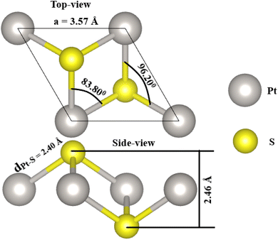
As a first step, the PtS2 monolayer geometry is optimized. Fig. 1 shows the optimized unit cell, which is fully described by the following structural parameters: (1) lattice constant a = 3.57 Å, which is in good agreement with previous calculations;56 (2) chemical bond length dPt–S = 2.40 Å; (3) total buckling height Δtotal = 2 × ΔPt–S = 2 × 1.23 = 2.46 Å; (4) interatomic angles ∠PtSPt = 96.20° and ∠SPtS = 83.80°. Then, the stability of the PtS2 monolayer is examined using the following criteria:• The phonon dispersion curves are calculated using the PHONOPY code.57 The results plotted in Fig. 2a show no obvious nonphysical imaginary frequency in the entire Brillouin zone, indicating that the PtS2 monolayer is dynamically stable.
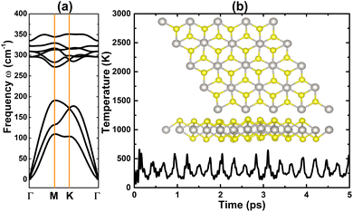 | ||
| Fig. 2 (a) Phonon dispersion curves and (b) AIMD simulations (variation of temperature + final atomic structure) at 300 K of the PtS2 monolayer. | ||
• Ab initio Molecular Dynamics (AIMD) simulations are performed at 300 K for 5 ps, using a 4 × 4 × 1 supercell. Herein, the NVT ensemble and Nose–Hoover thermostat are utilized.58,59Fig. 2b shows the variation of temperature and the final atomic structure. The stable fluctuation of temperature around 300 K can be noted. Moreover, no geometry reconstruction or broken Pt–S chemical bonds are noted, indicating that the structure is well preserved. These results indicate that the PtS2 monolayer is thermally stable.
• Using the energy-strain method, the elastic constants of the PtS2 monolayer are calculated. According to our calculations, its C11 and C12 constants have values of 88.57 and 23.26 N m−1, respectively, which can describe well the elasticity of 2D hexagonal symmetry. Importantly, the obtained elastic constants satisfy Born's criteria:60C11 > 0 and C11 > |C12|, indicating that the PtS2 monolayer is mechanically stable.
The electronic properties as well as interactions between the Pt and S atoms of the PtS2 monolayer are investigated using the optimized atomic structure. Fig. 3a shows the band structures obtained from PBE- and HSE06-based calculations. The HSE06 functional with a 25% fraction of the exact Hartree exchange potential is also utilized to calculate more accurately the monolayer band gap.61 Since the valence band maximum and conduction band minimum are located at different points as determined by both functionals, the PtS2 monolayer can be classified as a 2D indirect-gap semiconductor. The standard PBE functional provides an energy gap of 1.81 eV, while a larger (expected to be more accurate) value of 2.67 eV is obtained from HSE06-based computation. Note that these energy gaps are in line with results reported previously by several research groups,39,62 suggesting the reliability of our calculations. The projected density of states (PDOS) of both Pt and S atoms is given in Fig. 3b to analyze their contribution. Significant contributions of Pt-5d and S-3p orbitals in the considered energy range around the Fermi level can be noted. Moreover, their electronic states exhibit significant hybridization in both the valence band and the conduction band, giving evidence of the covalent Pt–S chemical bond. However, the difference in electronegativity between Pt and S atoms may cause charge transfer, forming ionic bonds. Specifically, Bader charge analysis implies that each S atom attracts a charge of 0.21 e from the Pt atom. Therefore, it can be concluded that the Pt–S chemical bonds in the PtS2 monolayer exhibit a mix of ionic and covalent characteristics.
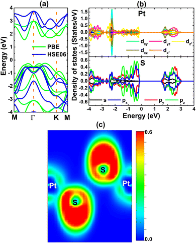 | ||
| Fig. 3 (a) Electronic band structure (the Fermi level is set to 0 eV), (b) projected density of states, and (c) electron localization function of the PtS2 monolayer. | ||
3.2 Effects of PtS3- and PtS6-type multivacancies
In this part, the effects of PtS3- and PtS6-type multivacancies (VaPtS3 and VaPtS6 systems) on the PtS2 monolayer electronic and magnetic properties are investigated. The atomic structures of these defected systems are visualized in Fig. S1 of the ESI.†Table 1 shows Ef values of 7.38 and 12.64 eV for VaPtS3 and VaPtS6 systems, respectively. These values correspond to 1.85 and 1.81 eV per atom for each single vacancy, respectively. The PtS2 monolayer exhibits good structural and chemical stability under the effects of multivacancies, which is confirmed by negative Ec values of −4.41 and −4.37 eV per atom, respectively. However, these values are less negative than that of the perfect PtS2 monolayer (−4.53 eV per atom), suggesting a slight reduction in the stability.| E f | E c | E g | ΔQ | M t | M l | |
|---|---|---|---|---|---|---|
| VaPtS3 | 7.38 | −4.41 | M/0.42 | — | 1.90 | — |
| VaPtS6 | 12.64 | −4.37 | M/M | — | 0.00 | — |
| DVO3 | −2.06 | −4.53 | M/1.27 | 0.76 | 1.00 | 0.83/−0.08 |
| DCrO3 | −1.52 | −4.45 | 0.83/1.25 | 0.85 | 2.00 | 2.37/−0.13 |
| DMnO3 | −1.36 | −4.47 | 0.80/1.17 | 1.07 | 3.00 | 3.80/−0.08 |
| DFeO3 | −0.36 | −4.49 | M/1.16 | 1.07 | 4.00 | 3.92/0.02 |
| DVO6 | −3.41 | −4.57 | 1.23/1.49 | 2.99 | 1.00 | 1.12/−0.03 |
| DCrO6 | −2.81 | −4.49 | M/1.51 | 3.17 | 2.00 | 2.79/−0.11 |
| DMnO6 | −1.81 | −4.49 | 1.52/0.82 | 3.03 | 3.00 | 3.76/−0.14 |
| DFeO6 | −1.05 | −4.52 | 1.52/0.09 | 3.06 | 5.99 | 4.27/0.20 |
Significant magnetization of the PtS2 monolayer induced by creating PtS3-type multivacancies is found. The emergence of magnetism is confirmed by the difference in charge distribution between spin channels. Specifically, this difference leads to a total magnetic moment of 1.90 μB. The spin density illustrated in Fig. 4 indicates that the magnetic properties of the VaPtS3 system are produced mainly by first S atoms from vacancy sites, where a small contribution from second Pt atoms and third S atoms is also observed. In contrast, no magnetism is obtained for the VaPtS6 system, indicating the preservation of the non-magnetic nature of the PtS2 monolayer when creating PtS6-type nanoholes.
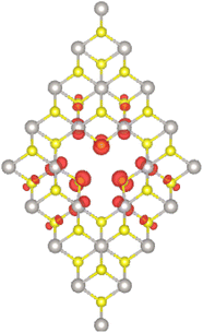 | ||
| Fig. 4 Spin density (iso-surface value: 0.005 e Å−3) in the PtS2 monolayer with PtS3-type vacancies. | ||
Fig. 5 shows the spin-polarized band structures of VaPtS3 and VaPtS6 systems. From the figure, one can see new middle-gap energy states created by vacancy defects that determine the system electronic behavior. It is important to mention that the unbalanced charge distribution is also reflected in the spin polarization of the VaPtS3 system band structure, while that of the VaPtS6 system is totally symmetric. These profiles are in agreement with the above analysis of magnetism. One of the PtS2 monolayer spin states is metallized under the effects of PtS3-type multivacancies, while the semiconductor character is preserved in the other one. Therefore, the VaPtS3 system can be classified as a 2D half-metallic material. Thus, creating PtS3-type multivacancies is an effective method to functionalize PtS2 monolayers for spintronic applications.63 In contrast, the VaPtS6 system exhibits a non-magnetic metallic nature considering the metallization of both spin states.
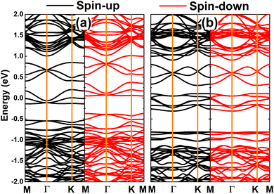 | ||
| Fig. 5 Spin-polarized band structure (the Fermi level is set to 0 eV) of the PtS2 monolayer with (a) PtS3- and (b) PtS6-type vacancies. | ||
The origin of middle-gap states is studied through the PDOS spectra of Pt and S atoms closest to vacancy sites. From Fig. 6a, one can see that the spin-up metallic character of the VaPtS3 system is generated mainly by Pt-dxy, Pt-dyz, and S-pz states. The spin-down band gap is regulated by the hybridization between Pt-dxz and S-pz states, which also produces the system magnetism as suggested by their strong spin polarization in the vicinity of the Fermi level. In the case of the VaPtS6 system, Pt-dyz and S-pz states cause mainly monolayer metallization (see Fig. 6b).
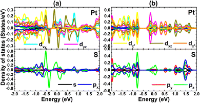 | ||
| Fig. 6 Projected density of states of atomic species around the defect sites of the PtS2 monolayer with (a) PtS3- and (b) PtS6-type vacancies. | ||
3.3 Effects of doping with TMO3 clusters
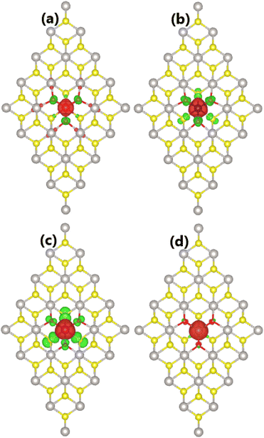
Herein, the effects of doping with TMO3 (DTMO3 system) clusters on the PtS2 monolayer electronic and magnetic properties are investigated. The calculated formation energy and cohesive energy are given in Table 1. Our calculations provide negative Ef values of −2.06, −1.52, −1.36, and −0.36 eV for DVO3, DCrO3, DMnO3, and DFeO3 systems, respectively. These results indicate the exothermic character of the doping process. The doping process is less favorable according to the increase of the atomic number of transition metals since the formation energy becomes less negative in this direction. Moreover, negative Ec values between −4.53 and −4.45 eV per atom imply that all four DTMO3 systems are structurally and chemically stable, where the incorporation of clusters reduces only slightly the monolayer stability.Our calculations confirm the significant magnetization of the PtS2 monolayer upon doping with TMO3 clusters. Total magnetic moments of 1.00, 2.00, 3.00, and 4.00 μB are obtained for DVO3, DCrO3, DMnO3, and DFeO3 systems, respectively. As expected, the system magnetism is produced mainly by TM atoms as suggested by the illustration of spin density in Fig. 7. From the figure, one can see large spin surfaces centered at TM sites. Moreover, small iso-surfaces are also observed near O and S atoms, indicating their small contribution to the system magnetism. It is important to note the antiparallel spin orientation between TM atoms and their neighboring O and S atoms.
The magnetism of DTMO3 systems is also reflected in the spin polarization as observed in their band structures displayed in Fig. 8. The electronic nature of the doped systems is determined by doping-induced middle-gap energy states. Specifically, DVO3 and DFeO3 are half-metallic 2D systems considering their metallic spin-up state and semiconductor spin-down state. Herein, the spin-down energy gaps of 1.27 and 1.16 eV are obtained, respectively. Additionally, a diluted magnetic semiconductor nature emerges in the PtS2 monolayer when doping with CrO3 and MnO3 clusters. In these cases, the spin-up/spin-down band gaps of 0.83/1.25 and 0.80/1.17 eV are obtained for DCrO3 and DMnO3 systems, respectively. These results suggest that feature-rich electronic and magnetic properties desired for spintronic applications can be induced in the PtS2 monolayer by doping with TMO3 clusters.64
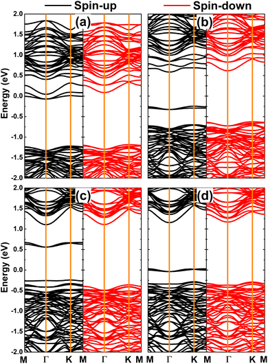 | ||
| Fig. 8 Spin-polarized band structure (the Fermi level is set to 0 eV) of the PtS2 monolayer doped with (a) VO3, (b) CrO3, (c) MnO3, and (d) FeO3 clusters. | ||
The calculated charge density difference confirms the charge depletion at TM atoms and charge accumulation at their neighboring O and S atoms (see Fig. S2 of the ESI†). The Bader charge is analyzed focusing on the constituent atoms of clusters. It is found that V, Cr, Mn, and Fe atoms lose charge amounts of 1.76, 1.61, 1.45, and 1.42 e, respectively. Meanwhile, each O atom of VO3, CrO3, MnO3, and FeO3 clusters gains a charge of 0.84, 0.82, 0.84, and 0.83 e, respectively. Therefore, it can be concluded that the host monolayer loses charge, transferring 0.76, 0.85, 1.07, and 1.07 e to VO3, CrO3, MnO3, and FeO3 clusters, respectively.
Fig. 9 shows the PDOS spectra of TM and O atoms of the clusters to study their contribution in the vicinity of the Fermi level, where TM-3d and O-2p orbitals are most prominent. Note that TM-dxy − dyz − dz2 and P-pz states primarily contribute to the metallic character of the spin-up state in the DVO3 and DFeO3 systems. As expected, the 3d orbital of transition metals exhibits strong spin polarization around the Fermi level to confirm their key role in producing the system magnetism.
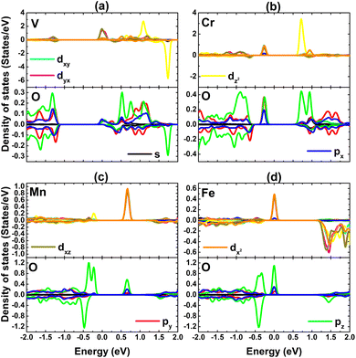 | ||
| Fig. 9 Projected density of states of cluster atomic species of the PtS2 monolayer doped with (a) VO3, (b) CrO3, (c) MnO3, and (d) FeO3 clusters. | ||
3.4 Effects of doping with TMO6 clusters
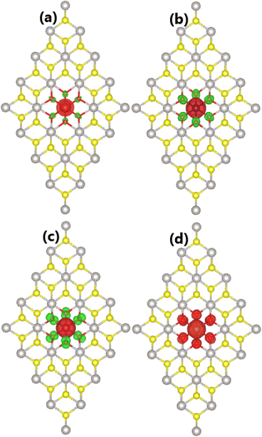
Now, the effects of doping with TMO6 (DTMO6 system) clusters on the PtS2 monolayer electronic and magnetic properties are investigated. Similar to previous cases of doping with TMO3 clusters, negative Ef values suggest an exothermic doping process. Specifically, Ef values of −3.41, −2.81, −1.81, and −1.05 eV are obtained for DVO6, DCrO6, DMnO6, and DFeO6 systems, respectively. Note that the formation energy becomes less negative when switching the transition metal from V to Fe, indicating the reduction of energetic favorability in this direction. Once formed, all the doped systems may have good structural and chemical stability as suggested by negative Ec values between −4.57 and −4.49 eV per atom, which are quite similar to that of the bare PtS2 monolayer.By calculating the difference in charge distribution between spin configurations, total magnetic moments of 1.00, 2.00, 3.00, and 5.99 μB are obtained for DVO6, DCrO6, DMnO6, and DFeO6 systems, respectively. Fig. 10 illustrates the spin density in these cluster-doped systems, which confirms that magnetic properties are produced mainly by the incorporated clusters. The iso-surface size indicates the key role of transition metals, where a smaller contribution from O atoms is also noted. Note that TM atoms and O atoms in DVO6, DCrO6 and DMnO6 systems exhibit an antiparallel spin orientation. In contrast, parallel spin ordering is observed for Fe atoms and O atoms in the DFeO6 system, resulting in a total magnetic moment that is much larger than that of the remaining three systems.
According to the emergence of the magnetism in the PtS2 monolayer, doping with TMO6 clusters leads to strong spin polarization in the electronic band structures as displayed in Fig. 11. Note that the spin symmetry breaking takes place mainly in the vicinity of the Fermi level of DTMO6 systems, where new middle-gap energy branches regulate their system electronic nature. The band structure profiles imply the diluted magnetic semiconductor nature of DVO6, DMnO6 and DFeO6 systems. In these cases, spin-up/spin-down energy gaps of 1.23/1.49, 1.52/0.82, and 1.52/0.09 eV are obtained, respectively. Moreover, the feature-rich half-metallicity is achieved by doping with CrO6 clusters, where the DCrO6 system has a metallic spin-up state and a semiconductor spin-down state with an energy gap of 1.51 eV. Such diluted magnetic semiconductor and half-metallic characteristics make DTMO6 systems prospective 2D candidates for spintronic applications.64
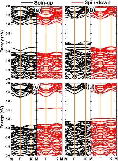 | ||
| Fig. 11 Spin-polarized band structure (the Fermi level is set to 0 eV) of the PtS2 monolayer doped with (a) VO6, (b) CrO6, (c) MnO6, and (d) FeO6 clusters. | ||
To investigate the interactions between clusters and their environment, the charge density difference is calculated. Charge depletion at TM sites and those Pt atoms around clusters is found, while charge enrichment is noted at O sites (see Fig. S3 of the ESI†). This feature indicates the charge gaining of O atoms, which is because of their more electronegative nature as compared to TM and Pt atoms. Focusing on the clusters, our Bader charge analysis indicates that the TM/O atoms of VO6, CrO6, MnO6, and FeO6 cluster have an effective ionic charge of +1.93/−0.82, +1.63/−0.80, +1.71/−0.79, and +1.74/−0.80 e (“+”: charge losing; “−”: charge gaining), respectively. The results indicate that these clusters gain a charge of −2.99, −3.17, −3.03, and −3.06 e from the host PtS2 monolayer, respectively.
The PDOS spectra of TM and O atoms are given in Fig. 12. In the considered energy range, TM-3d and O-2p orbitals make the main contributions. The metallic character of the DCrO3 system spin-up state is derived mainly from the O-pz state. The degree of spin polarization also indicates the key role of TM atoms in producing magnetic properties, with additionalcontributions coming from the pz state of their neighboring O atoms.
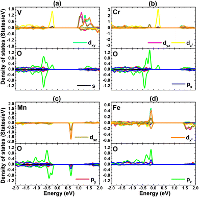 | ||
| Fig. 12 Projected density of states of cluster atomic species of the PtS2 monolayer doped with (a) VO6, (b) CrO6, (c) MnO6, and (d) FeO6 clusters. | ||
4 Conclusions
In summary, the effects of doping with TMOn clusters on the electronic and magnetic properties of PtS2 monolayers have been systematically investigated using first-principles calculations. The dynamical, thermal, and mechanical stability of the PtS2 monolayer is confirmed. It is a 2D indirect-gap semiconductor material, whose Pt–S chemical bonds exhibit a mix of covalent and ionic characteristics. The non-magnetic nature is preserved by creating PtS6-type multivacancies, where the monolayer becomes a metallic 2D material. In contrast, significant magnetism is achieved under the effects of PtS3-type multivacancies, where the pz state of S atoms around the vacancy sites is primarily responsible for magnetic properties. Interestingly, feature-rich half-metallicity is obtained for the VaPtS3 system. Similarly, the monolayer is significantly magnetized by doping with TMOn clusters. Feature-rich diluted magnetic semiconductor or half-metallic behaviors are obtained, depending on the nature of TMOn clusters. In these cases, electronic and magnetic properties are regulated mainly by TM-3d and O-2p orbitals. An antiparallel spin orientation in VO3, CrO3, MnO3, FeO3, VO6, CrO6, and MnO6 clusters has also been found, resulting in total magnetic moments between 1.00 and 4.00 μB. Meanwhile, the FeO6 cluster exhibits parallel spin ordering, resulting in a large total magnetic moment of 5.99 μB. Once incorporated substitutionally into the PtS2 monolayer, TMOn clusters act as charge gainers, attracting significant charge from the host monolayer. Our study suggests that new potential spintronic 2D materials can be made from PtS2 monolayers through doping with TMOn clusters.Data availability
Data related to this study are available upon reasonable request.Conflicts of interest
The authors declare that they have no known competing financial interests or personal relationships that could have appeared to influence the work reported in this paper.Acknowledgements
The calculations were performed at the DGCTIC-UNAM Supercomputing Center (projects LANCAD-UNAM-DGTIC-368). D. M. Hoat expresses his gratitude for all the valuable support from Duy Tan University, which is going to celebrate its 30th anniversary of establishment (Nov. 11, 1994 – Nov. 11, 2024) towards “Integral, Sustainable and Stable Development”.References
- E. C. Ahn, 2D materials for spintronic devices, npj 2D Mater. Appl., 2020, 4(1), 17 CrossRef CAS.
- Y. P. Feng, L. Shen, M. Yang, A. Wang, M. Zeng, Q. Wu, S. Chintalapati and C.-R. Chang, Prospects of spintronics based on 2D materials, Wiley Interdiscip. Rev.: Comput. Mol. Sci., 2017, 7(5), e1313 Search PubMed.
- B. Huang, G. Clark, E. Navarro-Moratalla, D. R. Klein, R. Cheng, K. L. Seyler, D. Zhong, E. Schmidgall, M. A. McGuire and D. H. Cobden, et al., Layer-dependent ferromagnetism in a van der Waals crystal down to the monolayer limit, Nature, 2017, 546(7657), 270–273 CrossRef CAS PubMed.
- C. Gong, L. Li, Z. Li, H. Ji, A. Stern, Y. Xia, T. Cao, W. Bao, C. Wang and Y. Wang, et al., Discovery of intrinsic ferromagnetism in two-dimensional van der Waals crystals, Nature, 2017, 546(7657), 265–269 CrossRef CAS PubMed.
- Y. Deng, Y. Yu, Y. Song, J. Zhang, N. Z. Wang, Z. Sun, Y. Yi, Y. Z. Wu, S. Wu and J. Zhu, et al., Gate-tunable room-temperature ferromagnetism in two-dimensional Fe3GeTe2, Nature, 2018, 563(7729), 94–99 CrossRef CAS PubMed.
- Z. Lin, B. R. Carvalho, E. Kahn, R. Lv, R. Rao, H. Terrones, M. A. Pimenta and M. Terrones, Defect engineering of two-dimensional transition metal dichalcogenides, 2D Materials, 2016, 3(2), 022002 CrossRef.
- A. Avsar, A. Ciarrocchi, M. Pizzochero, D. Unuchek, O. V. Yazyev and A. Kis, Defect induced, layer-modulated magnetism in ultrathin metallic PtSe2, Nat. Nanotechnol., 2019, 14(7), 674–678 CrossRef CAS PubMed.
- O. V. Yazyev and L. Helm, Defect-induced magnetism in graphene, Phys. Rev. B, 2007, 75(12), 125408 CrossRef.
- D. Shen, B. Zhao, Z. Zhang, H. Zhang, X. Yang, Z. Huang, B. Li, R. Song, Y. Jin and R. Wu, et al., Synthesis of group VIII magnetic transition-metal-doped monolayer MoSe2, ACS Nano, 2022, 16(7), 10623–10631 CrossRef CAS PubMed.
- M. Fan, J. Wu, J. Yuan, L. Deng, N. Zhong, L. He, J. Cui, Z. Wang, S. K. Behera and C. Zhang, et al., Doping nanoscale graphene domains improves magnetism in hexagonal boron nitride, Adv. Mater., 2019, 31(12), 1805778 CrossRef PubMed.
- K. Kang, S. Fu, K. Shayan, Y. Anthony, S. Dadras, X. Yuzan, F. Kazunori, M. Terrones, W. Zhang and S. Strauf, et al., The effects of substitutional Fe-doping on magnetism in MoS2 and WS2 monolayers, Nanotechnology, 2020, 32(9), 095708 CrossRef PubMed.
- V. V. Kulish, O. I. Malyi, C. Persson and P. Wu, Adsorption of metal adatoms on single-layer phosphorene, Phys. Chem. Chem. Phys., 2015, 17(2), 992–1000 RSC.
- O. Üzengi Aktürk, E. Aktürk and S. Ciraci, Effects of adatoms and physisorbed molecules on the physical properties of antimonene, Phys. Rev. B, 2016, 93(3), 035450 CrossRef.
- W. Li, M. Zhao, Y. Xia, R. Zhang and Y. Mu, Covalent-adsorption induced magnetism in graphene, J. Mater. Chem., 2009, 19(48), 9274–9282 RSC.
- L. Fu, K. Zhang, W. Zhang, J. Chen, Y. Deng, Y. Du and N. Tang, Synthesis and intrinsic magnetism of bilayer graphene nanoribbons, Carbon, 2019, 143, 1–7 CrossRef CAS.
- Y. Li, Z. Zhou, S. Zhang and Z. Chen, MoS2 nanoribbons: high stability and unusual electronic and magnetic properties, J. Am. Chem. Soc., 2008, 130(49), 16739–16744 CrossRef CAS PubMed.
- V. Barone and J. E. Peralta, Magnetic boron nitride nanoribbons with tunable electronic properties, Nano Lett., 2008, 8(8), 2210–2214 CrossRef CAS PubMed.
- S. Prucnal, A. Hashemi, M. Ghorbani-Asl, R. Hübner, J. Duan, Y. Wei, D. Sharma, D. R. Zahn, R. Ziegenrücker and U. Kentsch, et al., Chlorine doping of MoSe2 flakes by ion implantation, Nanoscale, 2021, 13(11), 5834–5846 RSC.
- M. N. Bui, S. Rost, M. Auge, J.-S. Tu, L. Zhou, I. Aguilera, S. Blügel, M. Ghorbani-Asl, A. V. Krasheninnikov and A. Hashemi, et al., Low-energy se ion implantation in MoS2 monolayers, npj 2D Mater. Appl., 2022, 6(1), 42 CrossRef CAS.
- J. Zhou, J. Lin, H. Sims, C. Jiang, C. Cong, J. A. Brehm, Z. Zhang, L. Niu, Y. Chen and Y. Zhou, et al., Synthesis of Co-doped MoS2 monolayers with enhanced valley splitting, Adv. Mater., 2020, 32(11), 1906536 CrossRef CAS PubMed.
- T. Wu, H. Shen, L. Sun, B. Cheng, B. Liu and J. Shen, Nitrogen and boron doped monolayer graphene by chemical vapor deposition using polystyrene, urea and boric acid, New J. Chem., 2012, 36(6), 1385–1391 RSC.
- D. M. Hoat, R. Ponce-Perez, C. V. Ha and J. Guerrero-Sanchez, Controlling the electronic and magnetic properties of the GeAs monolayer by generating Ge vacancies and doping with transition-metal atoms, Nanoscale Adv., 2024, 6, 3602–3611 RSC.
- J. Ren, H. Zhang and X. Cheng, Electronic and magnetic properties of all 3d transition-metal-doped ZnO monolayers, Int. J. Quantum Chem., 2013, 113(19), 2243–2250 CrossRef CAS.
- P. T. Bui, V. Van On, J. Guerrero-Sanchez and D. Hoat, Functionalization of boron phosphide monolayers for spintronic applications by doping with alkali and alkaline earth metals, J. Phys. D: Appl. Phys., 2024, 57(13), 135310 CrossRef.
- B. N. N. Thi, C. V. Ha, N. T. H. Lien, J. Guerrero-Sanchez and D. Hoat, Doping-mediated electronic and magnetic properties of graphene-like ionic NaX (X= F and Cl) monolayers, Phys. Chem. Chem. Phys., 2023, 25(47), 32569–32577 RSC.
- H. Zheng, J. Zhang, B. Yang, X. Du and Y. Yan, A first-principles study on the magnetic properties of nonmetal atom doped phosphorene monolayers, Phys. Chem. Chem. Phys., 2015, 17(25), 16341–16350 RSC.
- A.-M. Hu, L.-l. Wang, W.-Z. Xiao, G. Xiao and Q.-Y. Rong, Electronic structures and magnetic properties in nonmetallic element substituted MoS2 monolayer, Comput. Mater. Sci., 2015, 107, 72–78 CrossRef CAS.
- M. Chhowalla, Z. Liu and H. Zhang, Two-dimensional transition metal dichalcogenide (TMD) nanosheets, Chem. Soc. Rev., 2015, 44(9), 2584–2586 RSC.
- N. Huo, Y. Yang and J. Li, Optoelectronics based on 2D TMDs and heterostructures, J. Semicond., 2017, 38(3), 031002 CrossRef.
- H. Li, J. Wu, Z. Yin and H. Zhang, Preparation and applications of mechanically exfoliated single-layer and multilayer MoS2 and WSe2 nanosheets, Acc. Chem. Res., 2014, 47(4), 1067–1075 CrossRef CAS PubMed.
- L. Ottaviano, S. Palleschi, F. Perrozzi, G. D'Olimpio, F. Priante, M. Donarelli, P. Benassi, M. Nardone, M. Gonchigsuren and M. Gombosuren, et al., Mechanical exfoliation and layer number identification of MoS2 revisited, 2D Materials, 2017, 4(4), 045013 CrossRef.
- X. Wang, Y. Gong, G. Shi, W. L. Chow, K. Keyshar, G. Ye, R. Vajtai, J. Lou, Z. Liu and E. Ringe, et al., Chemical vapor deposition growth of crystalline monolayer MoSe2, ACS Nano, 2014, 8(5), 5125–5131 CrossRef CAS PubMed.
- F. G. Aras, A. Yilmaz, H. G. Tasdelen, A. Ozden, F. Ay, N. K. Perkgoz and A. Yeltik, A review on recent advances of chemical vapor deposition technique for monolayer transition metal dichalcogenides (MX2: Mo, W; S, Se, Te), Mater. Sci. Semicond. Process., 2022, 148, 106829 CrossRef CAS.
- Y. Wang, L. Zhou, M. Zhong, Y. Liu, S. Xiao and J. He, Two-dimensional noble transition-metal dichalcogenides for nanophotonics and optoelectronics: Status and prospects, Nano Res., 2022, 15(4), 3675–3694 CrossRef.
- X. Yu, P. Yu, D. Wu, B. Singh, Q. Zeng, H. Lin, W. Zhou, J. Lin, K. Suenaga and Z. Liu, et al., Atomically thin noble metal dichalcogenide: a broadband mid-infrared semiconductor, Nat. Commun., 2018, 9(1), 1545 CrossRef PubMed.
- C. Long, Y. Liang, H. Jin, B. Huang and Y. Dai, PdSe2: flexible two-dimensional transition metal dichalcogenides monolayer for water splitting photocatalyst with extremely low recombination rate, ACS Appl. Energy Mater., 2018, 2(1), 513–520 CrossRef.
- D. Zhao, S. Xie, Y. Wang, H. Zhu, L. Chen, Q. Sun and D. W. Zhang, Synthesis of large-scale few-layer PtS2 films by chemical vapor deposition, AIP Adv., 2019, 9(2), 025225 CrossRef.
- J. Lu, X. Zhang, G. Su, W. Yang, K. Han, X. Yu, Y. Wan, X. Wang and P. Yang, Large-area uniform few-layer PtS2: Synthesis, structure and physical properties, Mater. Today Phys., 2021, 18, 100376 CrossRef CAS.
- R. A. B. Villaos, C. P. Crisostomo, Z.-Q. Huang, S.-M. Huang, A. A. B. Padama, M. A. Albao, H. Lin and F.-C. Chuang, Thickness dependent electronic properties of Pt dichalcogenides, npj 2D Mater. Appl., 2019, 3(1), 2 CrossRef.
- G. Liu, Y. Gan, R. Quhe and P. Lu, Strain dependent electronic and optical properties of PtS2 monolayer, Chem. Phys. Lett., 2018, 709, 65–70 CrossRef CAS.
- Y. Ji, Y. Liu, Y. Xu, L. Liu and Y. Chen, Electronic and optical properties of sulfur vacancy-defect monolayer PtS2: A first-principles study, Mater. Chem. Phys., 2020, 255, 123588 CrossRef CAS.
- H. Yoo, K. Heo, M. H. R. Ansari and S. Cho, Recent advances in electrical doping of 2D semiconductor materials: Methods, analyses, and applications, Nanomaterials, 2021, 11(4), 832 CrossRef CAS PubMed.
- D. Li, Y. Niu, H. Zhao, C. Liang and Z. He, Electronic and magnetic properties of 3d-metal trioxides superhalogen cluster-doped monolayer MoS2: a first-principles study, Phys. Lett. A, 2014, 378(22–23), 1651–1656 CrossRef CAS.
- N. Feng, W. Mi, Y. Cheng, Z. Guo, U. Schwingenschlögl and H. Bai, First principles prediction of the magnetic properties of Fe-X6 (X= S, C, N, O, F) doped monolayer MoS2, Sci. Rep., 2014, 4(1), 3987 CrossRef PubMed.
- M. Rafique, Y. Shuai, H.-P. Tan and M. Hassan, Structural, electronic and magnetic properties of 3d metal trioxide clusters-doped monolayer graphene: a first-principles study, Appl. Surf. Sci., 2017, 399, 20–31 CrossRef CAS.
- W. Kohn and L. J. Sham, Self-consistent equations including exchange and correlation effects, Phys. Rev., 1965, 140(4A), A1133 CrossRef.
- G. Kresse and J. Furthmüller, Efficiency of ab-initio total energy calculations for metals and semiconductors using a plane-wave basis set, Comput. Mater. Sci., 1996, 6(1), 15–50 CrossRef CAS.
- G. Kresse and J. Furthmüller, Efficient iterative schemes for ab initio total-energy calculations using a plane-wave basis set, Phys. Rev. B: Condens. Matter Mater. Phys., 1996, 54(16), 11169 CrossRef CAS PubMed.
- J. P. Perdew, K. Burke and M. Ernzerhof, Generalized gradient approximation made simple, Phys. Rev. Lett., 1996, 77(18), 3865 CrossRef CAS PubMed.
- S. L. Dudarev, G. A. Botton, S. Y. Savrasov, C. Humphreys and A. P. Sutton, Electron-energy-loss spectra and the structural stability of nickel oxide: An LSDA+U study, Phys. Rev. B, 1998, 57(3), 1505 CrossRef CAS.
- Y. Wang, S. Li and J. Yi, Transition metal-doped tin monoxide monolayer: a first-principles study, J. Phys. Chem. C, 2018, 122(8), 4651–4661 CrossRef CAS.
- T. V. Vu, V. H. Chu, J. Guerrero-Sanchez and D. M. Hoat, Regulating the electronic and magnetic properties of a SnSSe janus monolayer toward optoelectronic and spintronic applications, ACS Appl. Electron. Mater., 2024, 6(5), 3647–3656 CrossRef CAS.
- H. J. Monkhorst and J. D. Pack, Special points for Brillouin-zone integrations, Phys. Rev. B: Solid State, 1976, 13(12), 5188 CrossRef.
- G. Henkelman, A. Arnaldsson and H. Jónsson, A fast and robust algorithm for Bader decomposition of charge density, Comput. Mater. Sci., 2006, 36(3), 354–360 CrossRef.
- E. Sanville, S. D. Kenny, R. Smith and G. Henkelman, Improved grid-based algorithm for Bader charge allocation, J. Comput. Chem., 2007, 28(5), 899–908 CrossRef CAS PubMed.
- M. Kashif, N. Anjum, A. Shahzad, A. Rasheed, M. Imran and A. Manzoor, Tuning the electronic and optical properties of the ZrS2/PtS2 van der Waals heterostructure by an external electric field and vertical strain, ACS omega, 2022, 7(37), 33453–33460 CrossRef CAS PubMed.
- A. Togo, L. Chaput, T. Tadano and I. Tanaka, Implementation strategies in phonopy and phono3py, J. Phys.: Condens. Matter, 2023, 35(35), 353001 CrossRef CAS PubMed.
- S. Nosé, A unified formulation of the constant temperature molecular dynamics methods, J. Chem. Phys., 1984, 81(1), 511–519 CrossRef.
- W. G. Hoover, Canonical dynamics: Equilibrium phase-space distributions, Phys. Rev. A: At., Mol., Opt. Phys., 1985, 31(3), 1695 CrossRef PubMed.
- F. Mouhat and F.-X. Coudert, Necessary and sufficient elastic stability conditions in various crystal systems, Phys. Rev. B: Condens. Matter Mater. Phys., 2014, 90(22), 224104 CrossRef.
- A. V. Krukau, O. A. Vydrov, A. F. Izmaylov and G. E. Scuseria, Influence of the exchange screening parameter on the performance of screened hybrid functionals, J. Chem. Phys., 2006, 125(22), 224106 CrossRef PubMed.
- M. Sajjad, N. Singh and U. Schwingenschlögl, Strongly bound excitons in monolayer PtS2 and PtSe2, Appl. Phys. Lett., 2018, 112(4), 043101 CrossRef.
- I. Choudhuri, P. Bhauriyal and B. Pathak, Recent advances in graphene-like 2D materials for spintronics applications, Chem. Mater., 2019, 31(20), 8260–8285 CrossRef CAS.
- X. Li and J. Yang, First-principles design of spintronics materials, Natl. Sci. Rev., 2016, 3(3), 365–381 CrossRef CAS.
Footnote |
| † Electronic supplementary information (ESI) available. See DOI: https://doi.org/10.1039/d4na00465e |
| This journal is © The Royal Society of Chemistry 2024 |

