 Open Access Article
Creative Commons Attribution 3.0 Unported Licence
Achieving ultra-low contact barriers in MX2/SiH (M = Nb, Ta; X = S, Se) metal–semiconductor heterostructures: first-principles prediction†
Son T.
Nguyen
a,
Chuong V.
Nguyen
 *b,
Huynh V.
Phuc
 c,
Nguyen N.
Hieu
 de and
Cuong Q.
Nguyen
 *de
*de
aFaculty of Electrical Engineering, Hanoi University of Industry, Hanoi 100000, Vietnam. E-mail: nguyensontung@haui.edu.vn
bDepartment of Materials Science and Engineering, Le Quy Don Technical University, Hanoi 100000, Vietnam. E-mail: chuong.vnguyen@lqdtu.edu.vn
cDivision of Physics, School of Education, Dong Thap University, Cao Lanh 870000, Vietnam
dInstitute of Research and Development, Duy Tan University, Da Nang 550000, Vietnam. E-mail: nguyenquangcuong3@duytan.edu.vn
eFaculty of Natural Sciences, Duy Tan University, Da Nang 550000, Vietnam
First published on 26th July 2024
Abstract
Minimizing the contact barriers at the interface, forming between two different two-dimensional metals and semiconductors, is essential for designing high-performance optoelectronic devices. In this work, we design different types of metal–semiconductor heterostructures by combining 2D metallic MX2 (M = Nb, Hf; X = S, Se) and 2D semiconductor SiH and investigate systematically their electronic properties and contact characteristics using first principles calculations. We find that all the MX2/SiH (M = Nb, Ta; X = S, Se) heterostructures are energetically stable, suggesting that they could potentially be synthesized in the future. Furthermore, the generation of the MX2/SiH metal–semiconductor heterostructures leads to the formation of the Schottky contact with ultra-low Schottky barriers of a few tens of meV. This finding suggests that all the 2D MX2 (M = Nb, Ta; X = S, Se) metals act as effective electrical contact 2D materials to contact with the SiH semiconductor, enabling electronic devices with high charge injection efficiency. Furthermore, the tunneling resistivity of all the MX2/SiH (M = Nb, Ta; X = S, Se) MSHs is low, confirming that they exhibit high electron injection efficiency. Our findings underscore fundamental insights for the design of high-performance multifunctional Schottky devices based on the metal–semiconductor MX2/SiH heterostructures with ultra-low contact barriers and high electron injection efficiency.
1 Introduction
Recently, two-dimensional (2D) materials, including graphene,1 transition metal dichalcogenides (TMDCs),2 phosphorene3 and MXenes,4 have garnered significant interest in the scientific community owing to their intriguing physical properties. Among these 2D materials, considerable attention has recently been directed towards TMDCs owing to their versatility in physical properties.5 Most TMDC 2D materials, such as MoS2,2 MoSe2,6 WS2,7 and WSe2,8 exhibit semiconducting characteristics. Unlike these semiconductors, NbS2, NbSe2, TaS2 and TaSe2 monolayers exhibit metallic behaviors. Recently, it has been discovered that these 2D metals serve as effective electrodes when integrated with other 2D semiconductors, facilitating the creation of metal/semiconductor heterostructures (MSHs) with significantly reduced contact barriers.9–12 For instance, Fu et al.9 successfully grew high-quality and clean NbS2/MoS2 MSH via one-step chemical vapor deposition (CVD). Tsoutsou et al.11 demonstrated that the TaSe2 monolayer could form low barrier contacts with other semiconductors, including HfSe2 and MoSe2 due to the small difference in their work functions. Using first-principles prediction, Nguyen et al.12 found that integrating 2D metallic TaSe2 with semiconducting WSe2 monolayers leads to the creation of TaSe2/WSe2 MSH with small resistivity, having great potential for the fabrication of novel Schottky devices. The search for appropriate 2D semiconductors to contact with 2D MX2 (M = Nb, Ta; X = S, Se) monolayers is intensifying in recent years as researchers aim to uncover ideal combinations for enhancing electronic and optoelectronic device applications.More recently, silicane (SiH), a novel 2D material has been predicted by full hydrogenation of monolayer silicene on both sides.13,14 It should be noted that silicane can also be synthesized by mechanical exfoliation, a strategy that has been used to obtain germanane (GeH).15 Additionally, hydrogenation opens a band gap, stabilizes the structure and eliminates conductivity in the silicene monolayer.16 Moreover, the electronic, thermoelectric and optical properties of the SiH monolayer are sensitive to external conditions, including strains,17 electric fields18 and constructing heterostructures.19–22 Among those strategies, construction of heterostructures has been proven to be one of the most effective strategies to enhance the physical properties of the SiH monolayer. For instance, we previously investigated the electronic properties and carrier mobility of the BP/SiH heterostructure as well as the effect of an electric field. The combination of SiH and BP monolayers gives rise to an enhancement in the optical absorption and carrier mobility compared to the constituent monolayers. Sheng et al.23 combined the InSe/SiH heterostructure and demonstrated that such combination leads to an enhancement of photocatalytic efficiency. Furthermore, the combination between SiH and PtSe2 (ref. 24) or AlAs25 also leads to an enhancement in the absorption coefficient and photocatalytic properties. It is found that the physical properties of the SiH material can be tuned when it is combined with other 2D semiconductors. However, to date, the combination between SiH and other 2D metals has not yet been extensively investigated.
In this work, we design MX2/SiH MSHs (M = Nb, Ta; X = S, Se) by stacking the 2D MX2 (M = Nb, Ta; X = S, Se) metals above on top of the SiH semiconductor using first-principles calculations. It is demonstrated that all the 2D MX2/SiH (M = Nb, Ta; X = S, Se) metal–semiconductor heterostructures form the Schottky contact with ultra-low contact barriers of a few tens of meV. Our findings could provide fundamental insights and open an avenue for the design of high-performance multifunctional Schottky devices based on the metal–semiconductor MX2/SiH heterostructures with ultra-low contact barriers and high electron injection efficiency.
2 Computational methods
Our calculations, including geometric optimization and the calculations of the interface properties, were carried out using density functional theory (DFT) as implemented in the simulation Quantum Espresso package.26 The electron exchange and correlation energy were described using the generalized gradient approximation (GGA) within the Perdew–Burke–Ernzerhof (PBE) formulation.27 For more accurate results, the hybrid Heyd–Scuseria–Ernzerhof (HSE06) functional was employed to calculate the band gap of the 2D semiconductor.28 Furthermore, the long-range interactions that may exist in layered 2D materials were described by adding the DFT-D3 method.29 A vacuum thickness of 27 Å was added along the thickness of the heterostructures to avoid any spurious interactions. All atomic positions were relaxed until the energy and forces converged to 10−6 eV and 0.01 eV Å−1, respectively. The cut-off energy of 520 eV and a k-point mesh of 9 × 9 × 1 were used for all the calculations. It should be noted that the cut-off energy was gradually increased until the total energy converged to within a tolerance of less than 0.01 eV Å−1. Whereas, we used such k-point grids that balanced accuracy and computational cost, ensuring that the electronic structure calculations remained precise with changes in total energy below 0.01 eV Å−1.3 Results and discussion
We first examine the atomic structures and electronic properties of 2D MX2 (M = Nb, Ta; X = S, Se) metals and the SiH semiconductor. The atomic structures and band structures of these 2D materials are depicted in Fig. 1. The SiH monolayer exhibits a hexagonal atomic arrangement with a buckled structure, as illustrated in Fig. 1(a). The hydrogen atoms are passivized on both sides of silicon atoms. The lattice constant of the SiH monolayer is obtained as 3.86 Å, which is consistent with previous reports.18,23 Similarly, the MX2 (M = Nb, Ta; X = S, Se) monolayers also possess a hexagonal structure. One transition M (M = Nb, Ta) metal is sandwiched between two different chalcogenide X (X = S, Se) atoms on both sides. The lattice constants of NbS2, NbSe2, TaS2 and TaSe2 monolayers are calculated to be 3.31, 3.43, 3.31 and 3.44 Å, respectively. These values are also close to the experimental measurements and theoretical reports. Furthermore, we investigate the band structures of all the MX2 (M = Nb, Ta; X = S, Se) metals and the SiH semiconductor, as illustrated in Fig. 1(b). All the MX2 materials exhibit metallic characteristics with the band crossing the Fermi level. On the other hand, the SiH monolayer shows semiconducting behavior with an indirect band gap. The maxima of valence bands (VBM) and minima of conduction bands (CBM) of the SiH monolayer are located at the Γ and M point, respectively. The band gap of SiH is predicted to be 2.18 and 2.96 eV, as measured using PBE and HSE approaches, respectively. Moreover, the Fermi level of the SiH semiconductor is closer to the VBM than the CBM, indicating that the SiH monolayer is a p-type extrinsic semiconductor. Our results are in good agreement with previous predictions.25,30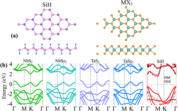 | ||
| Fig. 1 (a) Top and side views of the atomic structures and (b) band structures of monolayers SiH and MX2 (M = Nb, Ta; X = S, Se). The Fermi level is set to be zero. | ||
We further design the MX2/SiH MSHs by vertically stacking the 2D MX2 metals above on top of the 2D SiH semiconductor. The atomic structures of the MX2/SiH MSHs are depicted in Fig. 2 and S1 of the ESI.† We investigated four different stacking patterns (SP) of the MX2/SiH MSHs. The most energetically favorable SP is depicted in Fig. 2. To minimize the effects of strain caused by the lattice mismatch between the two different layers, the MX2/SiH MSHs are designed by using (2 × 2) and  supercells of MX2 and SiH layers, respectively. The overall lattice mismatch for the MX2/SiH MSHs is less than 2%. This value is still small and affects insignificantly the electronic properties of these 2D materials. After geometric optimization, the interlayer distances between the MX2 and SiH layers are obtained and listed in Table 1. The interlayer distances vary from 2.31 Å for the TaS2/SiH to 2.33 Å for the NbS2/SiH and to 2.37 Å for the TaSe2/SiH and to 2.39 Å for the NbSe2/SiH MSHs. This finding indicates that the interlayer distances in Nb(Ta)S2/SiH are shorter than those in the Nb(Ta)Se2/SiH MSH. In addition, we can find that these values of the interlayer distances in MX2/SiH heterostructures are comparable to those in other SiH-based heterostructures, such as AlAs/SiH,25 SiH/CdI2 (ref. 31) and InSe/SiH.23 Furthermore, we check the stability of all the MX2/SiH MSHs by calculating the binding energy as follows:
 | (1) |
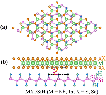 | ||
| Fig. 2 (a) Top view and (b) side views of the atomic structures of the MX2/SiH MS-vdWHs (M = Nb, Ta; X = S, Se). | ||
| a, Å | d, Å | E b, meV Å−2 | Φ p, eV | Φ n, eV | Contact types | |
|---|---|---|---|---|---|---|
| NbS2/SiH | 6.62 | 2.33 | −14.50 | 0.010 | 2.15 | p-ShC |
| NbSe2/SiH | 6.80 | 2.39 | −12.61 | 0.024 | 2.15 | p-ShC |
| TaS2/SiH | 6.63 | 2.32 | −14.17 | 0.014 | 2.14 | p-ShC |
| TaSe2/SiH | 6.81 | 2.37 | −12.72 | 0.067 | 2.12 | p-ShC |
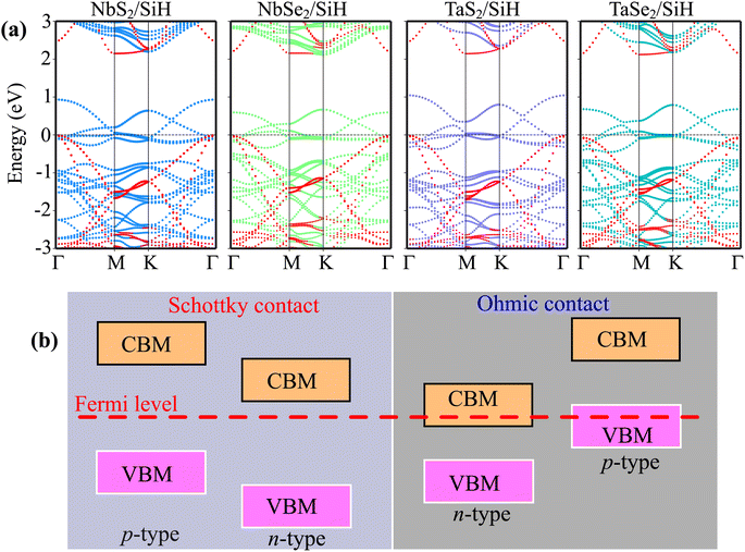
The projected band structures of the MX2/SiH (M = Nb, Ta; X = S, Se) MSHs are depicted in Fig. 3(a). One can find that the band structures of the MX2/SiH MSHs appear to be a sum of the band structures of the constituent MX2 metal and SiH semiconductor. More interestingly, the combination between MX2 metals and the SiH semiconductor leads to generation of metal/semiconductor heterostructures. Depending on the position of the band edges of the semiconductor relative to the Fermi level of metal, the combined heterostructure can form either the Schottky contact (ShC) or ohmic contact (OhC), as illustrated in Fig. 3(b). By analyzing the projected band structures, we observe that all the MX2/SiH (M = Nb, Ta; X = S, Se) MSHs lead to generation of the Schottky contact. In the band structures of the MX2/SiH (M = Nb, Ta; X = S, Se) MSHs, the Fermi level of the MX2 metal lies between the band edges of the SiH semiconductor. In addition, we find that the VBM of the SiH semiconductor is closer to the Fermi level than its CBM, indicating that all the MX2/SiH (M = Nb, Ta; X = S, Se) MSHs exhibit the p-type Schottky contact. The Schottky contact barriers for the p-type and n-type Schottky contact (ShC) can be obtained as: Φp = EF – EVBM and Φn = ECBM – EF, where EVBM and ECBM, respectively, are the energy of the VBM and CBM of the semiconductor SiH. EF is the Fermi level of the MX2/SiH heterostructure. The contact barriers for the MX2/SiH MSHs are listed in Table 1. It is interesting that the p-type Schottky barriers in all the MX2/SiH (M = Nb, Ta; X = S, Se) MSHs are ultra-low. The NbS2/SiH MSH shows the smallest p-type Schottky barrier of 10 meV, while the largest Schottky barrier is observed in the TaSe2/SiH MSH, which is only 67 meV. The observed ultra-low contact barrier in the MX2/SiH (M = Nb, Ta; X = S, Se) MSHs indicates that the charge injection efficiency in these heterostructures is highly advantageous.35,36 Thereby, the 2D MX2 metals act as effective electrical contact 2D materials to contact with the SiH semiconductor, enabling electronic devices with high charge injection efficiency.
Furthermore, to examine the charge injection efficiency of all the MX2/SiH MSHs, we calculate the tunneling probability and contact tunneling resistivity as follows:37
 | (2) |
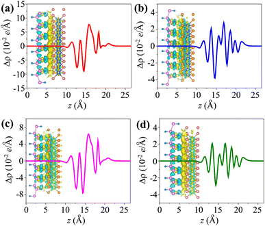
The wTB and ΦTB represent the tunneling width and tunneling height, which can be obtained by analyzing the electrostatic potential of the considered heterostructures. The electrostatic potentials of all the MX2/SiH (M = Nb, Ta; X = S, Se) MSHs are depicted in Fig. 4. The obtained tunneling probability and contact tunneling resistivity of all the MX2/SiH (M = Nb, Ta; X = S, Se) MSHs are listed in Table 2 and illustrated in Fig. 5. One can find that a higher tunneling probability is correlated with lower tunneling resistivity38 and enhanced electron injection. The tunneling probability of the NbSe2/SiH MSH is higher than that of the other heterostructures, suggesting that the NbSe2 2D metal acts as a superior electrical contact 2D material to contact with the SiH semiconductor to achieve high charge injection efficiency. Additionally, we find that the tunneling resistivity of all the MX2/SiH (M = Nb, Ta; X = S, Se) MSHs is as low as that of the low-contact-resistance Bi/MoS2.39,40 A lower tunneling resistivity correlates with a higher electron injection efficiency. Therefore, the electron injection efficiency in all the MX2/SiH MSHs is high. These findings suggest that the MX2 2D metals can act as promising electrodes for sub-10 nm field-effect transistors.41 Additionally, the work functions of NbS2, NbSe2, TaS2 and TaSe2 2D metals are calculated to be 6.12, 5.90, 5.51 and 5.36 eV. It is obvious that the work function of the MX2 monolayers is still higher than that for the common electrode graphene (4.6 eV).42 The large value of the work functions in the MX2 2D metals leads to an alignment towards the VBM of the 2D SiH semiconductor, forming a p-type Schottky contact.43
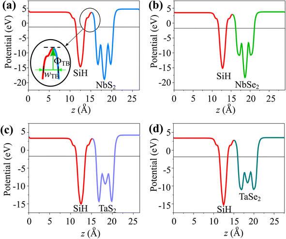 | ||
| Fig. 4 Calculated electrostatic effective potentials of (a) NbS2/SiH, (b) NbSe2/SiH, (c) TaS2/SiH and (d) TaSe2/SiH MSHs. | ||
 and contact tunneling resistivity of all the MX2/SiH (M = Nb, Ta; X = S, Se) MSHs
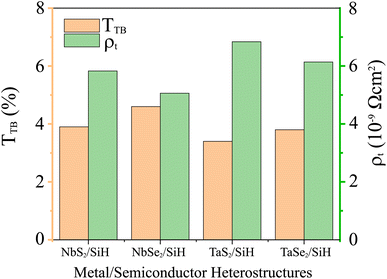 | ||
| Fig. 5 Calculated tunneling probability and contact tunneling resistivity of all the MX2/SiH (M = Nb, Ta; X = S, Se) MSHs. | ||
In addition, as illustrated in Fig. 4, we can see that the potential of the SiH layer is higher than that of the NbS(Se)2 layer in their corresponding MSHs, but it is deeper than the potential of the TaS(Se)2 layer. The charges flow from the layer with a deeper potential to the layer with a higher one. Therefore, electrons are transferred from the NbS(Se)2 layer to the SiH layer in the NbS(Se)2/SiH MSH. On the other hand, charges will flow from SiH to the TaS(Se)2 layer in the TaS(Se)2/SiH MSH.
We further calculated the charge density difference (CDD) in the MX2/SiH (M = Nb, Ta; X = S, Se) MSHs to visualize the charge redistribution and charge transfer between the two constituent monolayers. The CDD in the heterostructure can be obtained from the difference in the charge densities of the heterostructure (ρMSH) and the constituent metal (ρM) and semiconductor (ρS) as follows:
| Δρ = ρMSH − ρM − ρS | (3) |
The amount of charge transfer at the interface of MX2/SiH MSHs is obtained as:44,45
 | (4) |
The CDD for all the MX2/SiH (M = Nb, Ta; X = S, Se) MSHs is depicted in Fig. 6. Yellow and cyan regions indicate positive and negative charges, respectively. For the NbS2/SiH heterostructure, the positive charges are mainly accumulated in the NbS2 layer, while the negative charges are depleted in the SiH layer, as depicted in Fig. 6(a) and its inset. This finding indicates that the electrons are transferred from the NbS2 layer to the SiH layer, i.e. the metallic NbS2 layer loses electrons, while the semiconducting SiH layer gains them. A similar trend of charge transfer is also observed in the NbSe2/SiH MSH, as illustrated in Fig. 6(b). On the other hand, for the TaS(Se)2/SiH MSH, the positive charges are mainly accumulated on the side of the SiH layer, while the negative charges are depleted in the TaS(Se)2 layer. The electrons are transferred from the SiH layer to the TaS(Se)2 layer. From eqn (5), the amount of charge transfer at the interfaces of the NbS2/SiH, NbSe2/SiH, TaS2/SiH and TaSe2/SiH heterostructures is calculated to be 0.045, 0.012, 0.024 and 0.015e, respectively. Such amount of charge transfer is small, indicating that weak interactions are dominant at the interface of heterostructures. Furthermore, it should be noted that owing to the ultra-low Schottky barriers, the contact barriers and contact types in the MX2/SiH MSHs can be easily tuned by external conditions.46–51 For instance, applying a compressive strain of −3% includes a transition from Schottky to the ohmic contact in the NbS2/SiH heterostructure, as illustrated in Fig. S2 of the ESI.† The versatility in the contact behavior of the MX2/SiH MSHs under external conditions makes them promising candidates for next-generation multifunctional devices.
4 Conclusions
In summary, we have investigated the atomic structures, electronic properties and the formation of ultra-low contact barriers in the MX2/SiH (M = Nb, Ta; X = S, Se) MSHs using first-principles calculations. All the MX2/SiH (M = Nb, Ta; X = S, Se) MSHs are energetically stable, suggesting that these MSHs could potentially be synthesized in the future. More interestingly, the generation of the MX2/SiH metal–semiconductor heterostructures leads to the formation of the Schottky contact with ultra-low Schottky barriers of a few tens of meV. This finding suggests that all the 2D MX2 (M = Nb, Ta; X = S, Se) metals act as effective electrical contact 2D materials to contact with the SiH semiconductor, enabling electronic devices with high charge injection efficiency. Furthermore, the tunneling resistivity of all the MX2/SiH (M = Nb, Ta; X = S, Se) MSHs is low, confirming that they exhibit high electron injection efficiency. Our findings underscore fundamental insights for the design of high-performance multifunctional Schottky devices based on the metal–semiconductor MX2/SiH heterostructures with ultra-low contact barriers.Data availability
The data that support the findings of this study are available from the corresponding author upon reasonable request.Conflicts of interest
There are no conflicts to declare.References
- K. S. Novoselov, A. K. Geim, S. V. Morozov, D.-e. Jiang, Y. Zhang, S. V. Dubonos, I. V. Grigorieva and A. A. Firsov, Science, 2004, 306, 666–669 CrossRef PubMed
.
- B. Radisavljevic, A. Radenovic, J. Brivio, V. Giacometti and A. Kis, Nat. Nanotechnol., 2011, 6, 147–150 CrossRef PubMed
.
- A. Carvalho, M. Wang, X. Zhu, A. S. Rodin, H. Su and A. H. Castro Neto, Nat. Rev. Mater., 2016, 1, 1–16 Search PubMed
.
- K. R. G. Lim, M. Shekhirev, B. C. Wyatt, B. Anasori, Y. Gogotsi and Z. W. Seh, Nat. Synth, 2022, 1, 601–614 CrossRef
.
- W. Choi, N. Choudhary, G. H. Han, J. Park, D. Akinwande and Y. H. Lee, Mater. Today, 2017, 20, 116–130 CrossRef CAS
.
- X. Wang, Y. Gong, G. Shi, W. L. Chow, K. Keyshar, G. Ye, R. Vajtai, J. Lou, Z. Liu and E. Ringe,
et al.
, ACS Nano, 2014, 8, 5125–5131 CrossRef CAS PubMed
.
- C. Cong, J. Shang, X. Wu, B. Cao, N. Peimyoo, C. Qiu, L. Sun and T. Yu, Adv. Opt. Mater., 2014, 2, 131–136 CrossRef
.
- W.-T. Hsu, L.-S. Lu, D. Wang, J.-K. Huang, M.-Y. Li, T.-R. Chang, Y.-C. Chou, Z.-Y. Juang, H.-T. Jeng and L.-J. Li,
et al.
, Nat. Commun., 2017, 8, 929 CrossRef PubMed
.
- Q. Fu, X. Wang, J. Zhou, J. Xia, Q. Zeng, D. Lv, C. Zhu, X. Wang, Y. Shen and X. Li,
et al.
, Chem. Mater., 2018, 30, 4001–4007 CrossRef CAS
.
- P. Zhang, C. Bian, J. Ye, N. Cheng, X. Wang, H. Jiang, Y. Wei, Y. Zhang, Y. Du and L. Bao,
et al.
, Sci. China Mater., 2020, 1548–1559 CrossRef CAS
.
- D. Tsoutsou, K. E. Aretouli, P. Tsipas, J. Marquez-Velasco, E. Xenogiannopoulou, N. Kelaidis, S. Aminalragia Giamini and A. Dimoulas, ACS Appl. Mater. Interfaces, 2016, 8, 1836–1841 CrossRef
.
- S. T. Nguyen, N. N. Hieu, H. Phuc and C. V. Nguyen,
et al.
, Phys. Chem. Chem. Phys., 2024, 26, 9657–9664 RSC
.
- M. Houssa, E. Scalise, K. Sankaran, G. Pourtois, V. Afanasev and A. Stesmans, Appl. Phys. Lett., 2011, 98, 223107 CrossRef
.
- V. Zólyomi, J. Wallbank and V. Fal’ko, 2D Materials, 2014, 1, 011005 CrossRef
.
- E. Bianco, S. Butler, S. Jiang, O. D. Restrepo, W. Windl and J. E. Goldberger, ACS Nano, 2013, 7, 4414–4421 CrossRef CAS PubMed
.
- W. Wu, Z. Ao, C. Yang, S. Li, G. Wang and C. Li, J. Mater. Chem. C, 2015, 3, 2593–2602 RSC
.
- M. Manzoor, K. Kumar, A. K. Mishra, B. A. Al-Asbahi and R. Sharma, Solid State Commun., 2024, 115527 CrossRef CAS
.
- R. R. Banik, S. Ghosh and J. Chowdhury, J. Phys.: Condens. Matter, 2024, 36, 255706 CrossRef PubMed
.
- S.-T. Nguyen, C. V. Nguyen, K. Nguyen-Ba, H. Le-Quoc, N. V. Hieu and C. Q. Nguyen, RSC Adv., 2022, 12, 24172–24177 RSC
.
- S.-T. Nguyen, P. V. Cuong, C. Q. Nguyen and C. V. Nguyen, Phys. Chem. Chem. Phys., 2022, 24, 25144–25150 RSC
.
- P. Sang, Q. Wang, G. Yi, J. Wu, Y. Li and J. Chen, Appl. Surf. Sci., 2023, 614, 156170 CrossRef CAS
.
- L. Lv, X. Ma, W. Lou, X. Zhang, C. Shen, C. Xia and Y. Liu, Phys. Status Solidi B, 2022, 259, 2100666 CrossRef
.
- W. Sheng, Y. Xu, M. Liu, G. Nie, J. Wang and S. Gong, Phys. Chem. Chem. Phys., 2020, 22, 21436–21444 RSC
.
- S. Han, Y. Li and Z. Wang, Phys. Chem. Chem. Phys., 2020, 22, 17145–17151 RSC
.
- S. Han, Y. Li and Z. Wang, Phys. E, 2021, 134, 114869 CrossRef
.
- P. Giannozzi, S. Baroni, N. Bonini, M. Calandra, R. Car, C. Cavazzoni, D. Ceresoli, G. L. Chiarotti, M. Cococcioni and I. Dabo,
et al.
, J. Phys.: Condens.Matter, 2009, 21, 395502 CrossRef PubMed
.
- J. P. Perdew, K. Burke and M. Ernzerhof, Phys. Rev. Lett., 1996, 77, 3865 CrossRef CAS PubMed
.
- J. Heyd, G. E. Scuseria and M. Ernzerhof, J. Chem. Phys., 2003, 118, 8207–8215 CrossRef CAS
.
- S. Grimme, J. Antony, S. Ehrlich and H. Krieg, J. Chem. Phys., 2010, 132, 154104 CrossRef PubMed
.
- M. Niu, D. Cheng and D. Cao, Sci. Rep., 2014, 4, 4810 CrossRef CAS PubMed
.
- A. Priydarshi, A. Arora, Y. S. Chauhan, A. Agarwal and S. Bhowmick, J. Phys. Chem. C, 2023, 127, 21279–21288 CrossRef CAS
.
- J. Wang, Z. Guan, J. Huang, Q. Li and J. Yang, J. Mater. Chem. A, 2014, 2, 7960–7966 RSC
.
- K. Zhang, C. Ding, B. Pan, Z. Wu, A. Marga, L. Zhang, H. Zeng and S. Huang, Adv. Mater., 2021, 33, 2105079 CrossRef CAS
.
- Y. Zhang, Y. Yao, M. G. Sendeku, L. Yin, X. Zhan, F. Wang, Z. Wang and J. He, Adv. Mater., 2019, 31, 1901694 CrossRef
.
- Q. Wang, L. Cao, S.-J. Liang, W. Wu, G. Wang, C. H. Lee, W. L. Ong, H. Y. Yang, L. K. Ang and S. A. Yang,
et al.
, npj 2D Mater. Appl., 2021, 5, 71 CrossRef
.
- M. K. Mohanta, A. Arora and A. De Sarkar, Phys. Rev. B, 2021, 104, 165421 CrossRef
.
- C. C. Tho, S.-D. Guo, S.-J. Liang, W. L. Ong, C. S. Lau, L. Cao, G. Wang and Y. S. Ang, Appl. Phys. Rev., 2023, 10, 041307 Search PubMed
.
- Y. Wang, R. X. Yang, R. Quhe, H. Zhong, L. Cong, M. Ye, Z. Ni, Z. Song, J. Yang and J. Shi,
et al.
, Nanoscale, 2016, 8, 1179–1191 RSC
.
- P.-C. Shen, C. Su, Y. Lin, A.-S. Chou, C.-C. Cheng, J.-H. Park, M.-H. Chiu, A.-Y. Lu, H.-L. Tang and M. M. Tavakoli,
et al.
, Nature, 2021, 593, 211–217 CrossRef CAS
.
- T. Su, Y. Li, Q. Wang, W. Zhao, L. Cao and Y. S. Ang, J. Phys. D: Appl. Phys., 2023, 56, 234001 CrossRef
.
- C. W. Tan, L. Xu, C. C. Er, S.-P. Chai, B. Kozinsky, H. Y. Yang, S. A. Yang, J. Lu and Y. S. Ang, Adv. Funct. Mater., 2024, 34, 2308679 CrossRef CAS
.
- S. Naghdi, G. Sanchez-Arriaga and K. Y. Rhee, J. Alloys Compd., 2019, 805, 1117–1134 CrossRef CAS
.
- Y. Xiong, D. Xu, Y. Feng, G. Zhang, P. Lin and X. Chen, Adv. Mater., 2023, 35, 2206939 CrossRef CAS
.
- A. Arora, A. Rawat and A. De Sarkar, Phys. Rev. B, 2023, 107, 085402 CrossRef
.
- X.-H. Li, B.-J. Wang, X.-L. Cai, W.-Y. Yu, Y.-Y. Zhu, F.-Y. Li, R.-X. Fan, Y.-S. Zhang and S.-H. Ke, Nanoscale Res. Lett., 2018, 13, 1–10 CrossRef PubMed
.
- X. Gao, Y. Shen, Y. Ma, S. Wu and Z. Zhou, Comput. Mater. Sci., 2019, 170, 109200 CrossRef
.
- M. K. Mohanta and A. De Sarkar, Appl. Surf. Sci., 2021, 540, 148389 CrossRef
.
- F. Zhang, W. Li, Y. Ma and X. Dai, Solid State Commun., 2018, 271, 56–61 CrossRef CAS
.
- M. K. Mohanta and A. De Sarkar, Appl. Surf. Sci., 2020, 526, 146749 CrossRef CAS
.
- F. Zhang, W. Li, Y. Ma and X. Dai, Phys. E, 2018, 103, 284–288 CrossRef CAS
.
- W. Ai, Y. Shi, X. Hu, J. Yang and L. Sun, ACS Appl. Electron. Mater., 2023, 5, 5606–5613 CrossRef CAS
.
Footnote |
| † Electronic supplementary information (ESI) available. See DOI: https://doi.org/10.1039/d4na00482e |
| This journal is © The Royal Society of Chemistry 2024 |

