 Open Access Article
Modulations of the work function and morphology of a single MoS2 nanotube by charge injection†
Maja
Remškar
 *a,
Janez
Jelenc
a,
Nikolai
Czepurnyi
b,
Matjaž
Malok
 ac,
Luka
Pirker
 ad,
Rupert
Schreiner
b and
Andreas K.
Hüttel
 e
e
aSolid State Physics Department, Jozef Stefan Institute, Jamova ulica 39, SI-1000 Ljubljana, Slovenia. E-mail: maja.remskar@ijs.si
bFaculty of Applied Natural Sciences and Cultural Studies, OTH Regensburg, 93053 Regensburg, Germany
cFaculty of Mathematics and Physics, University of Ljubljana, Ljubljana SI-1000, Slovenia
dDepartment of Electrochemical Materials, J. Heyrovsky Institute of Physical Chemistry, Dolejskova 3, Prague 8, 182 23, Czech Republic
eInstitute for Experimental and Applied Physics, University of Regensburg, 93053 Regensburg, Germany
First published on 22nd July 2024
Abstract
Both the miniaturization of transistor components and the ongoing investigation of material systems with potential for quantum information processing have significantly increased current interest of researchers in semiconducting inorganic nanotubes. Here we report on an additional outstanding aspect of these nanostructures, namely the intrinsic coupling of electronic and mechanical properties. We observe electronic and morphology changes in a single MoS2 nanotube, exposed to charge injections by means of an atomic-force-microscopy tip. An elliptic deformation of the nanotube and helical twisting of the nanotube are visible, consistent with the reverse piezoelectric effect. Work-function changes are found to be dependent on the polarity of the injected carriers. An unexpected long-term persistence of the shape deformations is observed and explained with accumulation of structural defects and the resultant strain, which could cause a memory-like charge confinement and a long lasting modulation of the work function.
1. Introduction
MoS2 belongs to the group of transition-metal dichalcogenide crystals with a layered structure. It has recently attracted a lot of attention as a quasi-two-dimensional graphene analogue. Besides a plate-like morphology, spherical and cylindrical shapes have been reported.1–5 The unique growth of MoS2, directly from the vapour phase, leads to MoS2 nanotubes (NTs) with lengths up to several millimetres, and diameters from a few tens of nanometres up to several micrometers.2 Due to their slow synthesis over several weeks, growth takes place close to the chemical equilibrium, leading to a high degree of structural perfection. The resulting NTs support optical whispering-gallery modes,6 and represent a quantum-confinement environment for single-electron conductance.7 The crystal structure of MoS2 compound consists of S–Mo–S molecular layers with covalent bonds between atoms in a layer, and weak van der Waals interactions among the molecular layers. Due to the absence of dangling bonds on the basal (001) surfaces, an inertness and the absence of adsorbents are expected. In reality, the exposed (001) planes of MoS2 flat crystals were found to be n-doped due to the spontaneous formation of sulphur vacancies, causing surface-electron accumulation, which was nearly four orders of magnitude higher than in the inner bulk.8 The electrical conductance in MoS2 is highly anisotropic and varies from sample to sample, with 0.16 S cm−1 to 5.12 S cm−1 along the basal planes and 1.02 × 10⁻⁴ S cm−1 to 5.89 × 10⁻⁴ S cm−1 in the direction perpendicular to the (001) planes.9 The ratio between the conductance along the planes and that perpendicular to them is at least 103. In thin flakes (<10 μm), the conductance was found to be much larger and strongly dependent on the thickness,8i.e., it increased from 11 S cm−1 to 360 S cm−1 with a decrease in the thickness from 385 to 33 nm.Thin flakes of 2H-MoS2 composed of an odd number of S–Mo–S molecular layers show a piezoelectric response in line with theoretical predictions.10–12 Its intensity decreases with an increase in the number of layers. Strong piezoelectricity was also observed in 3R-MoS2, wherein two piezoelectric coefficients d33 (≈0.9 pm V−1 in an 18 nm thick flake) and d13 (≈1.6 pm V−1 in a 37 nm thick flake) were determined. There, the coefficients were found not to be apparently dependent on the thickness of the flakes.13 Piezoelectricity was theoretically predicted for a single-layer BN nanotube.14 There, a longitudinal piezoelectric response was proposed to exist in the zigzag NTs only under axial extension or compression. In the armchair NTs, conversely, the dipole moment is coupled only to the torsional strain. For chiral tubes, the elastic energy contains the product of the axial and torsional strains, and a tensile stress induces torsion and vice versa. In WS2 NTs, which are analogues to the MoS2 NTs, an in-plane sliding ferroelectricity was reported recently.15 It was explained by the piezoelectric nature of the asymmetric structure of the WS2 monolayers. Due to the change in piezoelectricity in the layers of different chirality, the shear force exceeding the friction force enables a mutual sliding and subsequent deformation of the NT.
This study presents the first experimental observation of the simultaneous shape and work-function (φ) modulations caused by a charge injection into a single MoS2 NT. Atomic force microscopy (AFM) probe was used to inject the current and to observe the topography changes. The contact potential difference (CPD) between the AFM tip and the NT was recorded by Kelvin-probe force microscopy (KPFM) before and after the injections of charges. The shape modifications of the NT are discussed in line of the reverse piezoelectric effect predicted for chiral tubular geometry with its radial and torsional components.14
2. Materials and methods
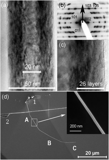
The MoS2 NTs under investigation and the MoS2 substrate were synthesized by a chemical transport reaction at 1010 K inside a quartz ampoule using iodine as the transport agent.2 Such NTs always grow in chiral mode, with the chiral angle in the range 10° to 16°.3 A homogeneous diameter of the NTs along several tens of microns indicates that the lattice structure does not consist of wrapped MoS2 monolayers, but that the layers are self-terminated to a form of cylinders. It is the elimination of the edge dangling bonds that stabilizes the cylindrical shape of these NTs. The stacking order of the molecular layers depends on the diameters of these tubes. The rhombohedral 3R stacking has been observed in tubes with diameters of more than 200 nm, while the hexagonal 2H stacking is typical for narrower tubes.4 The NT selected for the experiment, with a diameter of around 50 nm, belongs to the group of narrow nanotubes that crystalize in the 2H polytype. A detailed HRTEM structural characterization was performed on another NT of the same diameter (Fig. 1a). The wall thickness of the NT was about 30% of its diameter. The corresponding diffraction pattern taken from the whole diameter of the NT is an overlap of electrons diffracted from the basal planes, oriented from parallel to perpendicular to the electron beam. The chiral angle is 13° ± 1° (Fig. 1b). The diffraction pattern is indexed according to 2H-MoS2 (ICSD 03-065-0160). The wall consists of 26 molecular layers (Fig. 1b and c). Traces of amorphous material are visible on the outer surface of the NT. This contamination usually remains on the MoS2 NTs dispersed in ethanol, necessary specifically for drop-casting onto a TEM sample grid.The NT selected for the charge injection experiment was deposited on a MoS2 single crystal using an OmniProbe manipulator 200 (with a sharp tungsten tip) in a FEI Helios Nanolab 650 SEM-FIB microscope at 10−6 mbar. Platinum contacts were deposited in situ to keep the NT in place (Fig. 1d).
Charge injections were performed inside an ultra-high-vacuum atomic force microscope (VT-AFM Omicron, Germany). A Kelvin-probe force microscopy (KPFM) module was used to measure the contact potential difference (CPD) between the AFM tip, the NT, and the MoS2 single-crystal substrate. Since both the MoS2 NT and the MoS2 substrate can contain traces of iodine used in the transport reaction, leading to overall modification of the CPD, only relative values of the CPDs were taken into account. The current was injected in the following way. The NT was firstly located using the non-contact AFM (nc-AFM) with a Pt/Ir-coated silicon AFM tip (Type NSG10-Pt, NT-MDT, Spectrum Instruments) of a curvature radius ≈35 nm. By switching to the scanning tunnelling microscopy (STM) mode, the forced oscillations of the cantilever were stopped and the tip was auto-approached towards the sample until a pre-defined tunnelling current (200 pA) was established. Charge carriers were injected for 2 min under a bias from +2 V to +8 V or from −2 V to −8 V in 2 V steps. The current of 200 pA was maintained by the feedback loop. After the injections of holes at positive voltages applied to the AFM tip, a break was taken and then the electrons were injected at negative voltages. Relatively long breaks of 24 h or 48 h were taken with a purpose to relax the system before injection of other type of charge carriers. Shorter breaks were also used in some individual experiments.
Before and after each series of charge injections, the shape (topography) and the CPD image of the NT were recorded at three places: (i) near the surface step of the substrate (position A); (ii) in the central part of the NT (position B), and (iii) at the very end of the NT (position C) (Fig. 1d). The changes in the CPD profiles were normalized in such a way that the CPD of the substrate was nullified. Any tilting of AFM topography images was corrected using the max flatness tilt in SPIP 6.7.5. Line profiles were taken perpendicular to the NT's axis. Since the radius of the NT was smaller than the apex of the AFM tip, the precise lengths in these line profiles and thus the apparent diameters of the NT presented in the AFM images are not realistic. The nc-AFM images were taken at zero bias on the AFM tip.
3. Results
3.1. Charge injections at position C and their effects at positions B and A
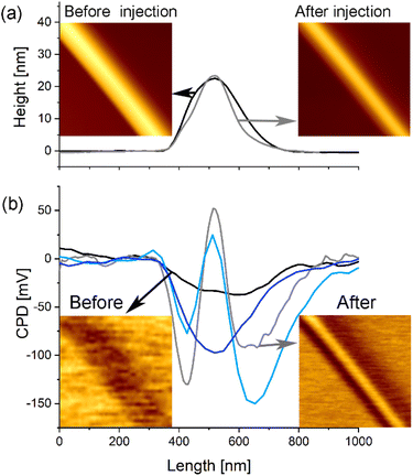
This has clearly changed after charge injections. A peak of up to 50 mV in height has appeared in the central part of the CPD profiles, surrounded by two minima of different depths. At A (grey in Fig. 2b), the left-hand minimum was deeper (−100 mV), while at B (light blue in Fig. 2b), the right-hand minimum was deeper (−150 mV). As discussed below, this spatial difference, together with the different degrees of asymmetry between the left- and right-hand minima are useful for a detailed discussion of the chiral deformation of the NT.
3.2. Charge injections and their effects at position B
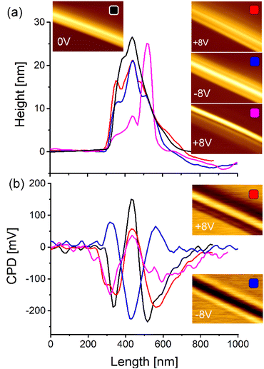
The wrinkling is likely due to the compression and simultaneous twisting of molecular layers with different radii; additionally, mutual sliding of adjacent molecular layers also cannot be excluded.15 For further observation of the shape deformations, it is important to note that the left-hand shoulder was higher than the right-hand one at this particular location and charge injection step, see the red curve in Fig. 3a.
After 48 h, electrons were injected at −2 V, −4 V, −6 V, and −8 V (see Fig. S3† for the intermediate steps). The shape of the NT was changed in a way that both shoulders decreased, but the left-hand shoulder was lower than the right-hand one (Fig. 3a – blue curve). This is an indication that the NT was exposed to a torsional strain, which turned the NT in an anti-clockwise direction. From the positions of the side peaks with respect to the centre of the NT at half the height of the central peak, we can estimate the angle of rotation to be around 30° (Fig. 3a).
After further 48 h, holes were injected again. In contrary to expectation, the NT continued to apparently rotate in the same direction as during the injection of electrons, with the right shoulder peak becoming stronger. This may be due to the incorporation of a so-far non-relaxed strain caused by the previous injection series. The final injection of holes at +8 V caused a drastic change in the NT's shape, and the right-hand shoulder then fully dominated the profile, while the central peak decreased by around 70%. The NT turned nearly perpendicularly to the substrate and became strongly deformed into a ribbon-like shape. The corresponding nc-AFM images are shown in the insets of Fig. 3a.
Before the first injection at B, a central peak of 150 mV and two side minima were recorded (Fig. 3b; black curve). The first injection of holes caused the suppression of the central peak in the CPD profile by 40% (Fig. 3b; red curve). The side valleys became shallower but wider. The CPD in the valleys was 150 mV (left-hand valley) and 190 mV (right-hand valley) below the CPD of the substrate. Qualitatively, however, the overall curve shape with a central maximum and two side minima is retained; consequently, we designate this the “holes-trapped shape”. After the injection of electrons 48 h later (Fig. 3b; blue curve), this changes and a deep central minimum of 225 mV occurred, surrounded by peaks of around 70 mV, the “electrons-trapped shape”. The injection of holes was then repeated after 48 h break (Fig. 3b; magenta curve), clearly restoring the shape with central peak and side minima; the ratio between right- and left-hand minima did however not recover to the situation after the first injection of holes (red curve). This reflects a degree of irreversibility of the topography deformations caused by the torsional component of the reverse piezoelectricity.
Regarding the initial conditions, the “holes-trapped” shape of the CPD in the black line of Fig. 3b indicates a memory effect, possibly caused by a charge trapped on structural defects and/or inbuilt lattice strain remaining from previously conducted charge injections.
The rotation of the NT in a direction that alternates from clockwise due to the injection of electrons to anti-clockwise due to the injection of holes, points towards the torsional component of the reverse piezoelectric effect as origin. The rotation angle likely depends on the chirality of the NT lattice and on the history of previous charge injections, which have caused strain in the lattice and accumulation of defects. Once deformed, the original shape of the NT is only partly retained due to some extend of plastic deformation (“shape-memory effect”). Only when a significantly greater force is applied it does “snap back”.
This also explains why the previous shape is not restored immediately when the reverse polarity is applied, but only when a higher voltage or another pulse at the same bias are applied. In addition, the NT was also progressively collapsing. The fact that the shape could not be recovered to the ideal cylindrical geometry leads to the conclusion that besides elastic deformations, which were stabilized by the charge retention, plastic deformations also occurred through the creation of structural defects and mutual gliding of molecular layers.15
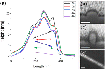
3.3. Further data on torsional deformation
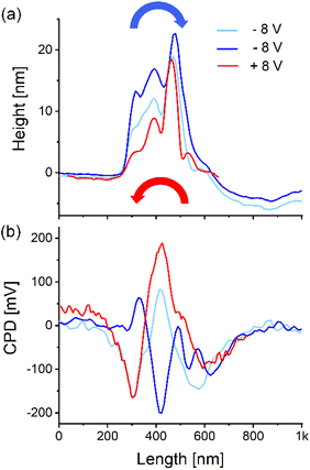
The complexity of the torsional deformation is shown in Fig. 5, which presents some profiles taken at the same place on the NT after consecutive electron injections at −2, −4, −6, and −8 V. The profiles are aligned on the middle peaks. Arrows represent the relative heights of the central peak shoulders. Because of the long-range elastic forces, the deformation at a certain place depends on the strain and plastic deformations of other parts of the NT. Nevertheless, rotation in the clockwise direction is visible, as are changes to the NT's width due to twisting.To further elucidate its shape, the NT was sliced via focussed ion beam (FIB) at different points along its length. The SEM micrographs of two cross-sections (Fig. 5b and c) clearly demonstrate deviations from the cylindrical geometry and given the differing angle of the long axis of the cross-sectional ellipsoid, confirm a torsional deformation of the NT. In addition, the top view of a part of the NT (Fig. 5d) reveals an increased concentration of secondary electrons along the NT's axis, which agrees with the model of wrinkling of the NT's wall, where a thicker band of material contributes to higher density of secondary electrons. Some parts of the NT in the same top-view are found feature less (see Fig. S4†). This is understood in a way that the distribution of the wrinkles was not uniform along the NT and that they could lie in different orientation with regard to the electron beam.
4. Discussion
A semiconducting MoS2 NT was placed onto a MoS2 single crystal substrate. Under electric contact, electrons were transferred from the NT to the grounded MoS2 substrate due to lower φ of the NT with respect to the φ of the substrate. Consequently, a potential barrier equal to the difference of both work functions has formed at the interface. Injection of charge carriers into the NT via a tunnelling contact disturbed the charge carrier equilibrium and local electrical charges were trapped in the NT at structural and electronic defects. Their presence caused the inverse piezoelectric effect with a deformation of the cylindrical shape of the NT and modulation of its work function.In general, injection of holes compressed the NT toward the substrate by 20%, while injection of electrons stretched it by 8% in opposite direction. The compression caused a wrinkling of the profile because of the compression of molecular layers with different radii and simultaneous twisting of them. The deformations due to reverse piezoelectric effect, do depend on the diameter of particular molecular layers.15 Therefore, the particular molecular layers inside the NT's wall with different circumference and energy of curvature were exposed to different degree of deformation. It was calculated that during compressive loading, the MoS2 nanotubes exhibit critical buckling stresses that scale inversely with increasing diameter.17 Different elastic constants in bulk MoS2, i.e., c11 along the basal planes (23.8 GPa) and c33 perpendicular to them (5.2 GPa)18 resist the isotropic reverse piezoelectric compression of the cylindrical shape. In addition, the chiral lattice structure makes the deformation of the NT even more complex. Both, the radial and torsion components of the stress are different in adjacent layers. The initial cylindrical shape became wrinkled forming the three-peaks profile (Fig. 4a) already during the first current injection. This indicates a weakening of the interaction among the molecular layers. A slipping among the molecular layers could contribute to the irreversibility of the reverse piezoelectric effect.15
While charge-induced lattice deformations were already reported for MoS2 monolayers,19 several unknowns were identified in the case of chiral MoS2 nanotube. Firstly, it is unclear why the trapped charge was maintained for such a long time (days) at room temperature, though the potential barrier at the NT/substrate interface could contribute to the electron confinement. It is possible that the inverse piezoelectric effect occurred only during the process of charge injection, when an electric current of ≈200 nA was flowing through the NT. A combination of torsional and radial components of the reverse piezoelectric effect caused elastic and plastic deformations in the NT lattice, resulting in a metastable shape of the NT. Due to the relatively thick NT's walls and the long-range order in radial direction which has to obey the 2H polytype stacking, one can expect very complex deformations and helical strain incorporated in the structure.
Such a mechanical state can be more stable than transient local charge distributions in a semiconducting environment alone. Therefore, we understand the metastable state of the NT as a kind of mechanical bi-stability. Once deformed, the shape is partly retained (“shape-memory effect”) and only when a significantly greater force is applied it “snaps back” as it is shown in the Fig. 4a. The helical strain causes the rotation of the NT in a direction depending on charge polarity, as expected for the torsional component of the reverse piezoelectric effect. The sense and degree of the rotation likely depend on the chirality of the NT lattice, on the in-built strain accumulated from previous charge injections, and on interaction strength with the substrate.
While the shape-memory effect, i.e. the retention of the morphology changes, can be explained with metastable elastic/plastic deformations and a need of a sufficiently strong force to jump from one to another metastable state, the dependence of the work function on polarity of injected charge carriers cannot be entirely explained with the strain effect. Injection of electrons caused a strong decrease of work function of the NT without prominent changes in topography (Fig. 3a – blue and red curves). The CPD profiles after injection of electrons and holes at the same absolute value of bias are opposite (Fig. 3b – blue and red curves). The results show that it is possible to increase the work function of the MoS2 NT for 150 mV by injection of holes and to decrease it for around 220 mV by injection of electrons at 8 V and −8 V bias, respectively. As the shape-memory effect, also these changes in work function persisted for days. This long-term work function enhancement due to injection of holes could be explained with inbuilt lattice strain according to the report that work function of MoS2 nano-sheets was linearly increased with in-plane tensile lattice strain.20 In analogy, after injection of electrons one can assume that the decrease of the work function is caused by the lattice compression. In the chiral structure of the NT, both kinds of deformations, i.e. tensile and compression strains are present simultaneously due to the torsion component of inverse piezoelectric effect. This is visible in the asymmetry and the positions of the side peaks in CPD profiles (Fig. 3b and 4b). The collapse of the cylindrical shape happened after injection of holes (Fig. 3b – pink curve, 4b – red curve), when the work function at the central part of the flattened NT was strongly enhanced revealing tensile strain, while the side edges were compressed and work function was decreased there. Injection of electrons partially recovered the pristine shape, the central part of the NT was exposed to compression (decrease of work function) and side parts to tensile strain (increase of work function).
While not discussed so far, the charge trapped in the potential well at the NT-substrate interface due to the different work functions of the MoS2 substrate and the MoS2 NTs cannot be excluded from consideration. The junction between the NT and the substrate forms a local p–n hetero-junction of two semiconductors and therefore a kind of 1D-potential well. The injection of electrons made the NT more n-type, while the injection of holes made the NT less n-type or even p-type. The minimum (after electrons injection) and maximum (after injection of holes) of CPD profiles are positioned along the NT-substrate interface projection (Fig. 3b). In literature, relatively long charge decay times (6.9 and 7.5 h) were reported for charge diffusion between MoS2 nano-sheets and Si/SiO2 substrate.21 Different values of the work function for both sidewalls are explained by the torsional deformation, which changes the relative orientation of the molecular layers and affects the internal strain. Besides electron confinement, the strain formed in the NT due to inverse piezoelectric effect contributes to the modulation of work function, as it was reported for the MoS2 grain boundaries.22 Such a tuning of work-function by a lasting mechanical strain can address a problem of high contact resistance in contact-engineering.23
5. Conclusions
In conclusion, electrons and holes were injected into a chiral MoS2 nanotube. The flow of charge carriers caused a deformation of the NT from cylindrical to a semi-elliptical and wrinkled shape. The NT became helically twisted along its axis and progressively plastically deformed with injections. These shape changes are explained by a coupling of the axial and torsional components of reverse piezoelectricity with a strength that depends on the diameter of a particular molecular layer, the chirality of the tubular structure and the history of previous injections of charge carriers. A shape-memory effect was observed and explained with a kind of metastable states with tensile and compression strains in-built in the lattice as a result of charge injections. The work function of the NT's sidewalls decreased after the injections of holes and increased after the injections of electrons. In contrast, the work function of the NT in its central part increased with the injection of holes and decreased with the injection of electrons. These results are important for elucidating the impact of locally trapped charges and their interplay with the nanomaterial shape in MoS2 nanotubes, for the development of nanotube-based transducers or torsional resonators, and for the understanding of reverse piezoelectricity in a chiral geometry.Data availability
The data supporting this article have been included as part of the ESI.†Author contributions
M. R. (funding acquisition, supervision-lead, writing – original draft); J. J. (methodology-lead, investigation-lead); N. C. (investigation, formal analysis); M. M. (conceptualization, methodology-minor); L. P. (methodology, editing); R. S. (supervision, writing – review & editing), A. K. H. (writing – review & Editing).Conflicts of interest
There are no conflicts to declare.Acknowledgements
The authors thank the Slovenian Research Agency for financial support via grants P1-0099 and PR-11224, and Deutsche Forschungsgemeinschaft for financial support via grants Hu 1808/4-1 (project id 438638106) and Hu 1808/6-1 (project id 438640730).Notes and references
- L. Margulis, G. Salitra, R. Tenne and M. Talianker, Nature, 1993, 365, 113 CrossRef CAS.
- M. Remskar, Z. Skraba, F. Cleton, R. Sanjines and F. Levy, Appl. Phys. Lett., 1996, 69, 351 CrossRef CAS.
- M. Remskar, A. K. Hüttel, T. V. Shubina, A. Seabaugh, S. Fathipour, R. Lawrowski and R. Schreiner, Isr. J. Chem., 2021, 61, e202100100 Search PubMed.
- M. Remskar, Z. Skraba, C. Ballif, R. Sanjines and F. Levy, Surf. Sci., 1999, 433/435, 637 CrossRef.
- M. Remskar, Adv. Mater., 2004, 16, 1 CrossRef.
- D. R. Kazanov, A. V. Poshakinskiy, V. Y. Davydov, A. N. Smirnov, I. A. Eliseyev, D. A. Kirilenko, M. Remškar, S. Fathipour, A. Mintairov, A. Seabaugh, B. Gil and T. V. Shubina, Appl. Phys. Lett., 2018, 113, 101106 CrossRef.
- R. T. K. Schock, J. Neuwald, W. Möckel, M. Kronseder, L. Pirker, M. Remškar and A. K. Hüttel, Adv. Mater., 2023, 35, 2209333 CrossRef CAS PubMed.
- M. D. Siao, W. C. Shen, R. S. Chen, Z. W. Chang, M. C. Shih, Y. P. Chiu and C. M. Cheng, Nat. Commun., 2018, 9, 1442 CrossRef CAS PubMed.
- S. R. Guha Thakurta and A. K. Dutta, Phys. Chem. Solids, 1983, 44, 407 CrossRef.
- K. A. N. Duerloo, M. T. Ong and E. J. Reed, J. Phys. Chem. Lett., 2012, 3, 2871 CrossRef CAS.
- H. Zhu, Y. Wang, J. Xiao, M. Liu, S. Xiong, Z. J. Wong, Z. Ye, Y. Ye, X. Yin and X. Zhang, Nat. Nanotechnol., 2015, 10, 151 CrossRef CAS PubMed.
- W. Wu, L. Wang, Y. Li, F. Zhang, L. Lin, S. Niu, D. Chenet, X. Zhang, Y. Hao, T. F. Heinz, J. Hone and Z. L. Wang, Nature, 2014, 514, 470 CrossRef CAS PubMed.
- H. Hallil, W. Cai, K. Zhang, P. Yu, S. Liu, R. Xu, C. Q. Xiong, Z. Liu and Q. Zhang, Adv. Electron. Mater., 2022, 8, 2101131 CrossRef CAS.
- N. Sai and E. J. Mele, Phys. Rev. B: Condens. Matter Mater. Phys., 2003, 68, 1 CrossRef.
- Y. Sun, S. Xu, Z. Xu, J. Tian, M. Bai, Z. Qi, Y. Niu, H. H. Aung, X. Xiong, J. Han, C. Lu, J. Yin, S. Wang, Q. Chen, R. Tenne, A. Zak and Y. Guo, Nat. Commun., 2022, 13, 5391 CrossRef CAS PubMed.
- F. Gossenberger, T. Roman, K. Forster-Tonigold and A. Groß, Beilstein J. Nanotechnol., 2014, 5, 152 CrossRef PubMed.
- E. W. Bucholz and S. B. Sinnott, J. Appl. Phys., 2012, 112, 123510 CrossRef.
- J. L. Feldman, J. Phys. Chem. Solids, 1976, 37, 1141 CrossRef CAS.
- A. Singh, G. Sharma, B. P. Singh and P. Vasa, J. Phys. Chem. C, 2019, 123, 17943 CrossRef CAS.
- J. Shakya, S. Kumar, D. Kanjilal and T. Mohanty, Sci. Rep., 2017, 7, 9576 CrossRef PubMed.
- R. Sanikop, N. Arya, V. Balakrishnan and C. Sudakar, J. Phys. Chem. C, 2021, 125, 12155 CrossRef CAS.
- M. Precner, T. Polaković, Q. Qiao, D. J. Trainer, A. V. Putilov, C. Di Giorgio, I. Cone, Y. Zhu, X. X. Xi, M. Lavarone and G. Karapetrov, Sci. Rep., 2018, 8, 6724 CrossRef CAS PubMed.
- N. K. Nepal, L. Yu, Q. Yan and A. Ruzsinszky, Phys. Rev. Mater., 2019, 3, 073601 CrossRef CAS.
Footnote |
| † Electronic supplementary information (ESI) available. See DOI: https://doi.org/10.1039/d4na00490f |
| This journal is © The Royal Society of Chemistry 2024 |

