 Open Access Article
Creative Commons Attribution 3.0 Unported Licence
Photocatalytic deposition of noble metals on 0D, 1D, and 2D TiO2 structures: a review
Salih
Veziroglu
 *ab,
Josiah
Shondo
a,
Tim
Tjardts
a,
Tamim B.
Sarwar
a,
Ayse
Sünbül
ac,
Yogendra Kumar
Mishra
 d,
Franz
Faupel
 ab and
Oral Cenk
Aktas
 *a
*a
aChair for Multicomponent Materials, Department of Materials Science, Faculty of Engineering, Kiel University, Kaiserstr. 2, 24143 Kiel, Germany. E-mail: sve@tf.uni-kiel.de; oca@tf.uni-kiel.de
bKiel Nano, Surface and Interface Science KiNSIS, Kiel University, Christian Albrechts-Platz 4, 24118, Kiel, Germany
cFraunhofer Institute for Photonic Microsystems IPMS, Center Nanoelectronic Technologies CNT, An der Bartlake 5, Dresden, 01109, Germany
dMads Clausen Institute, NanoSYD, University of Southern Denmark, Alsion 2, 6400 Sønderborg, Denmark
First published on 6th November 2024
Abstract
In recent years, extensive research on noble metal–TiO2 nanocomposites has demonstrated their crucial role in various applications such as water splitting, self-cleaning, CO2 reduction, and wastewater treatment. The structure of the noble metal–TiO2 nanocomposites is critical in determining their photocatalytic properties. Numerous studies in the literature describe the preparation of these nanocomposites with various shapes and sizes to achieve tunable photocatalytic performance. However, achieving a stable coupling between the noble metal and the TiO2 surface remains a challenge for long-term use. Photocatalytic deposition is one of the most promising approaches to obtain well-defined noble metal structures on TiO2 surfaces with strong adhesion. Noble metal nanoparticles (NPs) can be quickly grown on the TiO2 surface under light exposure. However, various parameters such as the pH, temperature, precursor, and electron sacrificial agent affect the size and distribution of the deposited particles. In this review article, we look at the critical parameters that influence the photocatalytic deposition of noble metals on major TiO2 morphologies, classified as 0D (NPs and nanocrystals), 1D (nanotubes and nanowires), and 2D (thin films).
1 Introduction
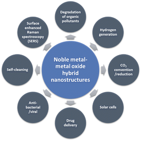
Over the last few decades, nanomaterials have attracted exceptional research interest due to their unique physical and chemical properties, mainly arising from their high surface area (enormous surface-to-volume ratios) and nanoscale size.1 Among the different kinds of nanomaterials, noble metal (Au, Ag, Pt, Pd, as well as the Au/Ag alloy) and metal oxide (TiO2, ZnO, Cu2O, and CeO2) nanocomposites with well-defined structures and properties have gained significant attention for many applications, especially in photocatalysis2 (degradation of organic pollutants,3 photocatalytic hydrogen generation, photocatalytic CO2 reduction, etc.), solar cells,4 biomedicine5 and surface-enhanced Raman spectroscopy (SERS) (Fig. 1).6,7 The effectiveness of these hybrid nanocomposites depends highly on their size,8 shape,4 and structure-dependent properties (e.g., surface and interface chemistry).9 Therefore, the rational design (new structures with specific functionality), well-controlled synthesis and detailed characterization, and a better understanding of structure–property relationships are crucial to the functionality of the nanocomposites and their use in real-world applications.10In the literature, several methods exist to prepare functional noble metal–metal oxide nanostructures, including impregnation,11 chemical vapor deposition,12 solvothermal synthesis,13 electrodeposition,14 atomic-layer deposition (ALD),15 sputtering,16 physical mixing,12 and green synthesis17 (Table 1). Among these methods, photocatalytic deposition (photodeposition or photoinduced reduction) is attractive due to its simplicity. It requires only illumination or irradiation to produce well-defined metal nanoparticles (NPs) in a simple reactor system without recourse to high temperature and cost. However, it requires some specific parameters, such as light intensity, to control the structure, size, surface coverage and oxidation state of the deposited NPs.18–20
| Method | Advantages | Disadvantages |
|---|---|---|
| Photodeposition | • Mild reaction conditions | • Requires specific light conditions (e.g., UV) |
| • Low cost and simple setup | • Limited to certain metals and substrates | |
| • Green and safe process | • May have lower deposition rates compared to other methods | |
| • Control over spatial distribution of nanoparticles | ||
| • Potential for various applications (photocatalysis, electrocatalysis, etc.) | ||
| Simple reduction process | • Low-cost and straightforward method | • Often requires additional reducing agents unless spontaneous reduction is used |
| • Can be performed under ambient conditions | • Control over particle size can be limited | |
| • Minimal equipment required | ||
| Chemical vapor deposition (CVD) | • High purity and uniformity of films | • High temperatures required |
| • Suitable for large-scale production | • Complex equipment setup | |
| • Good control over thickness | • Potentially hazardous chemicals involved | |
| Sputtering | • Versatile for different materials | • Requires vacuum conditions |
| • Good adhesion to substrates | • Can lead to non-uniform coatings | |
| • Can produce thin films with controlled thickness | • Equipment can be expensive | |
| Electrochemical deposition | • Low cost and simple setup | • Limited to conductive substrates |
| • Good control over morphology and composition | • May require post-deposition treatments for optimal properties | |
| • Can be done at room temperature | ||
| Laser ablation | • High control over particle size and shape | • Expensive equipment needed |
| • Fast processing times | • Limited scalability for mass production | |
| • Minimal contamination risk | ||
| Atomic layer deposition (ALD) | • Atomic-level control over thickness and composition | • Slow deposition rates |
| • Excellent uniformity on complex surfaces | • High cost of precursors and equipment |
In recent years, photodeposition has emerged as an ideal method in photocatalysis, with applications ranging from the degradation of organic pollutants and photocatalytic hydrogen generation to self-cleaning surfaces and photocatalytic CO2 reduction. Despite its widespread use, the precise origins of the term “photodeposition” remain unclear. One of the earliest recorded uses of this term can be traced back to a study by Sadowsky and Payne in 1957.21 The term was used to explain the deposition of a phosphor color screen for a cathode ray tube. Photodeposition involves irradiating a semiconductor (slurry, paste, powder, or a thin film) in metal salt solution resulting in metal nanoparticle deposition on the semiconductor surface. Photoexcited electrons from the semiconductor reduce the metal cations with suitable redox potential, resulting in the formation of metal nanoparticles on the semiconductor surface.22,23
Generally, in semiconductors, the magnitude of the band gap determines the electrical, electronic, and optical properties of the semiconductors. The band gap also defines the wavelength sensitivity of the semiconductors to light exposure. Photoexcitation with light of energy larger than the band gap energy promotes an electron from the valence band to the conduction band, creating an electronic vacancy or “hole” (h+) in the valence band (see eqn (1)).24
 | (1) |
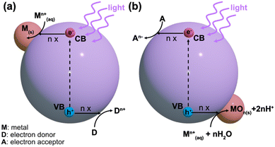
Typically, the energy level at the bottom of the conduction band determines the reducing ability of the photoelectrons, while the energy level at the top of the valence band determines the oxidizing ability of the photogenerated holes.25 Both of these species can be utilized in photocatalytic redox reactions. Normally, the conduction band electrons facilitate reduction reactions with the surrounding chemical species, while the valence band holes provide electron acceptors for photocatalytic oxidation.23 This understanding is critical for designing metal-supported catalysts via the photodeposition technique. For a successful photocatalytic reduction, the photocatalyst's conduction band edge should be more negative than the reduction reaction's standard potential on the NHE scale.23 Conversely, for successful photocatalytic oxidation, the valence band edge must be more positive than the corresponding reduction's standard potential. Photodeposition relies on photocatalytic redox reactions with precursor species, which is schematically shown in Fig. 2. In the photodeposition of metals, the corresponding generalized reduction reaction from a metal precursor ion Mn+ reduced by n conduction band electrons is given in eqn (2).23
| M(aq)n+ + ne− → M(s) | (2) |
Alternatively, in an oxidative counterpart reaction with n valence band holes and water, a metal oxide species is formed, as shown in eqn (3)23
| M(aq)n+ + nh+ + nH2O + MOn(s) + 2nH+ | (3) |
When a metal particle with a higher work function is in contact with an n-type semiconductor, electrons transfer from the semiconductor to the metal particle.26,27 Consequently, at the metal–semiconductor interface, a rectifying Schottky barrier is formed.28 This barrier facilitates charge separation by reducing the electron–hole recombination, thereby enhancing the photocatalytic activity of materials like TiO2.29 Because of the improved separation of electrons and holes, metal deposition on the semiconductor surface enhances photocatalytic reactions by hastening the transfer of electrons to reactants, such as dissolved oxygen molecules.30 The prediction of Schottky barrier formation and overall band structure typically relies on literature-reported or experimentally determined work functions as a starting point. However, the work function of metal oxide semiconductors like TiO2 is highly sensitive to experimental conditions, leading to a wide range of reported values.31,32 Moreover, the work functions can vary depending on factors such as crystallinity, particle geometry33,34 and the surrounding environment.32 This makes accurate predictions of band structure and Schottky barrier formation challenging as these properties are influenced by the crystal structure, morphology and the operational environment.
Among many semiconductor materials, TiO2 is one of the most suitable candidates for industrial applications due to its photoactivity, high chemical stability, eco-friendliness, and cost effectiveness. However, it has two drawbacks restricting its photocatalytic applications: limited photoresponse range (λ < 380 nm) and low quantum yields at longer wavelengths (λ > 400 nm). The quantum yield increases upon modification of the TiO2 surface with noble metals such as Au, Ag, Pt, and Pd due to the formation of a Schottky contact.20 Moreover, when the TiO2 surface is modified with noble metals, it can lead to a shift in the absorption edge of the TiO2 to the vis region (narrowing band gap). Also, localized surface plasmonic activity of the noble metals boosts the excitation of active charge carriers.35 Due to these synergetic effects of noble metals and TiO2, an enhancement in the photocatalytic activity is achieved, providing an excellent opportunity for industrial use under solar light illumination.36 Hence, photocatalytic deposition of noble metals and metal oxides on TiO2 has gained more attention in recent years because of its applications in photocatalytic solar fuel synthesis,37 wastewater treatment,38 air purification,24 self-cleaning,39,40 and biomedical applications.41
Photoinduced redox reactions at the surface of TiO2 have been known since the early 20th century. In 1920/21, Carl Renz reported observations of the darkening effect of TiO2 when exposed to sunlight.42 Later, it was shown that photoreactions with the surrounding medium, including exposure of TiO2 to light in the presence of silver nitrate (AgNO3), resulted in the reduction of AgNO3 to metallic Ag (deposition of Ag particles).43 A few decades later, Clark and Vondjidis reported infrared spectroscopy studies of TiO2 NPs mixed with AgNO3. They showed that AgNO3 was reduced to metallic Ag after UV irradiation of the mixture.44 However, the study, which was reported by Kraeutler and Bard in 1978, sparked much research interest in the photodeposition process.45 In this report, platinum (Pt) was photodeposited on TiO2 (anatase) by irradiating a paste containing anatase powder, hexachloroplatinic acid (H2PtCl6), hydrochloric acid (HCl), sodium carbonate (Na2CO3), and acetic acid (CH3COOH) as an electron scavenger. During the reaction process, the system was purged with nitrogen to remove O2 and CO2, and the temperature was increased to 55 °C. Finally, it was shown that well-dispersed Pt NPs could be obtained via photodeposition.
The photodeposition process has been known for more than 55 years in the scientific community. However, it is still a challenge to understand all process parameters to obtain well-desired structures for specific applications since several parameters need to be considered to allow the photodeposition process to occur on the semiconductor surface, such as the sacrificial reagent,46 pH,47 temperature,48 metal precursor,49 light exposure time50 and intensity,51 and absence or presence of oxygen in the media.23 To date, many research and review articles have concentrated on the effect of such photodeposition parameters, especially using TiO2.23,52–54 Only a few studies have focused on investigating the impact of the morphology of TiO2 on the photodeposition process, unlike other deposition parameters. The morphology directly influences the photodeposition process by affecting the specific/active surface area, availability of charge carriers, pore structure, crystalline phase, and exposed surface facet.55,56 Therefore, the morphology differences need to be considered as one of the key points to achieve well-desired photodeposited nanostructures on the TiO2 surface. As depicted in Fig. 3, variable morphologies of TiO2 are categorized as 0D: NPs and nanocrystals; 1D: nanotubes and nanowires; and 2D: thin films.
 | ||
| Fig. 3 Schematic illustration of the most used TiO2 morphologies (0D: NPs and nanocrystals; 1D: nanotubes and nanowires; and 2D: thin films). | ||
So far, numerous research articles have reported on the preparation of noble metals on TiO2 surfaces via photodeposition, highlighting the advantages of this approach.46,52,57,58 Additionally, excellent reviews have been published in the past few years on the photodeposition process that focused on the methods, mechanisms, and applications of photodeposition.23,59 In most cases, the authors have focused on the effect of deposition parameters, which include the sacrificial electron donors, pH, precursor, temperature, as well as the absence and presence of oxygen.23,59,60 However, a comprehensive review analyzing the role of various TiO2 morphologies in the catalytic activity and photodeposition processes is still lacking, hindering further advancement in photocatalytic research. Therefore, in this review article, we provide an overview of the recent research progress on the photodeposition of noble metals on different TiO2 morphologies such as 0D: NPs and nanocrystals; 1D: nanotubes and nanowires; and 2D: thin films. The following sections can give researchers different perspectives on the photodeposition process based on used materials and systems. Additionally, future perspectives on preparing future metal–semiconductor systems via photodeposition will be presented and discussed.
2 Photocatalytic deposition of noble metal nanoparticles on different TiO2 morphologies
2.1. 0D structures
| Properties | Units | Value |
|---|---|---|
| Specific surface area | m2 g−1 | 35–65 |
| Approximate particle size64 | Nm | 20 |
| pH value in 4% dispersion | — | 3.5–4.5 |
| Tapped density | g L−1 | 100–180 |
Research groups have provided detailed insights into the phase structure of P25 TiO2. It has been established that P25 TiO2 powder comprises multiphasic TiO2 nanoparticles (NPs), consisting of approximately 80% anatase and 20% rutile in the crystalline phase. Additionally, an amorphous phase has been identified through X-ray diffraction (XRD) analysis and transmission electron microscopy (TEM) measurements.64 It has been determined that the anatase to rutile ratio changes from batch to batch and should be somewhere between 70![[thin space (1/6-em)]](https://www.rsc.org/images/entities/char_2009.gif) :
:![[thin space (1/6-em)]](https://www.rsc.org/images/entities/char_2009.gif) 30 and 80
30 and 80![[thin space (1/6-em)]](https://www.rsc.org/images/entities/char_2009.gif) :
:![[thin space (1/6-em)]](https://www.rsc.org/images/entities/char_2009.gif) 20.65
20.65
P25 TiO2 has been frequently used as a substrate material for the photodeposition of noble metals, among other TiO2 NPs.30,46,58,67,68 Sclafani and Herrmann first demonstrated the growth of noble metals on P25 TiO2 in 1998.69 They reported the effect of grown Ag nanoparticles on the photocatalytic activity of TiO2, specifically rutile and anatase phases in both organic and aqueous media. Ag–P25 TiO2 samples were prepared via photocatalytic deposition by irradiating an aqueous AgNO3 solution with a 125 W high-pressure mercury lamp, using a 300 nm optical filter.69 Furthermore, the authors investigated the effect of deposited noble metals (Ag and Pt) as both single and bimetallic systems on the distinctive phases of P25. Notably, in the anatase phase, Pt selectively grows atop pre-existing Ag particles, showing 100% selectivity. Whereas, in the rutile phase, Pt can grow both on Ag particles and directly on the rutile surface. Additionally, the study showed that Ag deposits are beneficial for rutile activity but has detrimental effect on anatase activity.69
Over the past few decades, the photodeposition of noble metals on commercial P25 TiO2 has been investigated to improve control over the particle size, distribution, and morphology for specific applications.58,66 In this regard, Bhardwaj et al. studied the effects of different wt% of Ag loadings on commercial P25 TiO2 and different deposition times (30–90 min) on the structural, optical, and photocatalytic properties of Ag/TiO2 nanocomposites. The study showed that increasing the loading amount and UV irradiation time during photodeposition enhanced the plasmonic response, resulting in uniform nanostructure growth and regular distribution of Ag NPs.58
Pt is the most effective metal catalyst in conventional thermal oxidation processes among other noble metals. In particular, the loading of Pt onto the P25 TiO2 surface increases the efficiency of charge separation and promotes the amount of absorbed organic compound on the surface. Platinum (Pt) functions as an electron sink through the formation of a charge-transfer complex with TiO2. The catalytic properties of Pt are particularly influenced by several factors, including the nanoparticle size, dispersion, morphology, and oxidation state.52 Jiang et al.66 showed that methanol is critical for controlling Pt formation on P25 TiO2 during photodeposition. Their study investigated the role of methanol in the fabrication of Pt loaded on P25 TiO2 for photocatalytic H2 generation. Pt was deposited on TiO2 using chloroplatinic acid (H2PtCl6) as a precursor in an aqueous solution with various methanol concentrations under 300 W Xe lamp illumination with an intensity of 124.6 mW cm−2.66 It was found that the resulting H2 production rate increased linearly with the vol% of methanol used in the precursor solution. Fig. 4 shows bright-field high-resolution transmission electron microscopy (HRTEM) images of the resulting Pt-loaded P25 TiO2 NPs and the corresponding particle distributions. The dark spots in the bright-field HRTEM images can be associated with the Pt loading due to Z contrast. Fig. 4a-1 and a-2 exhibit the Pt-loaded P25 TiO2 surfaces when 100 vol% methanol was used during the deposition.
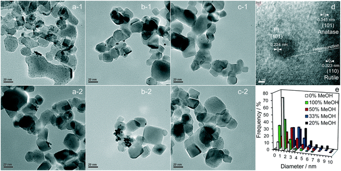 | ||
| Fig. 4 Representative bright-field HRTEM images of (a-1 and a-2) 100%, (b-1 and b-2) 20%, and (c-1 and c-2) 0% MeOH with 1 wt% Pt/TiO2, and (d) an individual Pt metal nanoparticle at the interface between anatase and rutile crystallites. (e) Particle size distributions as a function of methanol concentration during PD. Adapted with permission from ref. 66. Copyright (2016) Royal Society of Chemistry (RSC). | ||
When considering Z contrast, the small dark spots on the grey particles can be associated with highly dispersed small Pt NPs. Fig. 4b-1 and b-2 show the resulting Pt-loaded P25 TiO2 when 20 vol% methanol was used during deposition. Comparing these images to those of a 100 vol% sample, it was observed that the overall dispersion of the Pt NPs has decreased, and the overall size of the Pt NPs increased. For the samples prepared in a 0 vol% methanol solution, highly dispersed dark spots can be seen in the resulting HRTEM images shown in Fig. 4c-1 and c-2. Here, the dispersion and size of the samples appear comparable to those of the 100% vol sample. Fig. 4d depicts a Pt nanoparticle on the P25 TiO2 surface. Based on the structure of the crystallites present, it can be concluded that the Pt NPs grow at the interface between anatase and rutile crystallites, indicating no preferential substrate crystal phase. In fact, Jiang et al.66 reported that the Pt NPs were deposited randomly across the anatase and rutile surfaces of P25 TiO2. The particle distribution of Pt particles can be extracted from TEM images of particles with different vol% samples used during sample preparation, as shown in Fig. 4e. It can be observed that both 100 vol% and 0 vol% methanol lead to highly dispersed Pt NPs (mostly <2.5 nm), whereas 20 vol% methanol leads to larger Pt NPs (some >4 nm). Upon an increase in methanol from 20 vol% up to 100 vol%, a decrease in the overall particle size and an increase in the dispersion could be observed. This is consistent with the TEM images discussed above. The decrease in particle size and the increase in dispersion can be attributed to methanol acting as a hole scavenger, suppressing recombination in TiO2 during the photodeposition and leading to electron-rich surfaces where metallic Pt can be deposited. At 0 vol%, non-metallic Pt compounds like PtO2 and PtCl lead to high dispersion. Still, an increase in methanol concentration causes metallic Pt to be produced more frequently, initially leading to large metallic Pt NPs at low concentrations. The Pt loading shows more dispersion and a decrease in the size of particles as the methanol concentration increases. This leads to the conclusion that the photodeposition of Pt on P25 TiO2 methanol drives both Pt reduction and its subsequent redispersion.
Over the years, numerous studies have been published based on the photodeposition of noble metals on P25 TiO2 NPs for various applications (Table 3).22,30,46,53,57,58,66–68,70–73 Investigation of these data concludes that mercury lamps and sometimes xenon lamps were preferentially used to perform the photodeposition reactions. Usually, an aqueous AgNO3 solution is used as a precursor for the photodeposition of Ag NPs. However, different sacrificial agents can be used for specific purposes, such as varying particle sizes and surface coverages. Chlorine-based precursors such as H2PtCl6 and HAuCl4 solutions are commonly used to prepare Pt and Au NPs, respectively. These chlorine-based compounds are readily available and have high solubility in water.
| Deposited noble metal | UV source and wavelength (λ) | Precursor molecule; additional agent | Possible applications | Reported in |
|---|---|---|---|---|
| Ag | Mercury arc lamp, 125 W 10.4 mW cm−2, λ not given | AgNO3; isopropanol | Photodegradation of salicylic acid | Bhardwaj et al.58 |
| Ag | Xenon lamp, 300 W, λ not given | AgNO3; sodium hydrogen carbonate | Photocatalytic reduction of CO2 with water | Hammad et al.53 |
| Ag | Mercury lamp, 500 W, λ = 365 nm | AgNO3; methanol | Not given | Ma et al.70 |
| Ag | UV-A lamp, 40 W, λ = 350–400 nm | [Ag(S2O3)2]3 in radiographic wastewater | Bacterial disinfection | Wahyuni et al.71 |
| Ag and Pt | Mercury lamp, 200 W, λ = 365 nm | AgNO3 | Not given | Taing et al.57 |
| K2PtCl4 | ||||
| Trisodium citrate | ||||
| Pd | Low-pressure mercury lamp, 250 W m−2, λ not given | PdCl2; methanol | Organic photodegradation reactions | Dadsetan et al.68 |
| Pd | Low-pressure mercury lamp, 250 W m−2, λ not given | PdCl2; methanol, ethanol, ethylene glycol, and 1-isopropanol | Not given | Dadsetan et al.46 |
| Bimetallic Pd–Au | Mercury lamp, 6 W, λ = 254 nm | Pd(C5H7O2)2 | Selective oxidative esterification of methanol to form methyl formate | Colmenares et al.72 |
| HAuCl4·3H2O | ||||
| Acetonitrile | ||||
| Pt | Super-pressure mercury lamp, 30 mW cm−2, λ = 240–500 nm | H2PtCl6; methanol | Photocatalytic H2 evolution | Haselmann et al.30 |
| Pt | Xenon lamp, 300 W, λ not given | H2PtCl6; methanol | Photocatalytic H2 evolution | Jiang et al.66 |
| Au and Pt | Mercury lamp, 0.15 W m−2, λ = 365 nm | HAuCl4 | Not given | Galeano et al.73 |
| H2PtCl6 | ||||
| Isopropanol | ||||
| Au, Pt, and Rh | Mercury–xenon lamp, 200 W, λ not given | AuCl3 (Au2Cl6) | Not given | Ohyama et al.22 |
| H2PtCl6·6H2O | ||||
| RhCl3 | ||||
| Methanol | ||||
| Au, Pt, Rh, Pd, and Ag | High-pressure mercury arc lamp, λ > 300 nm | HAuCl4 | Water splitting without using any reagents under irradiation of visible light | Tanaka et al.67 |
| Colloidal Au nanoparticles | ||||
| Oxalic acid | ||||
| Other precursors not given |
![[thin space (1/6-em)]](https://www.rsc.org/images/entities/char_2009.gif) :
:![[thin space (1/6-em)]](https://www.rsc.org/images/entities/char_2009.gif) 30 have been utilized as excellent photocatalysts for photodecomposition of organic pollutants and solar-energy conversion due to their high photoactivity.77,78 In general, TiO2 has been shown to possess an anatase tetragonal bipyramidal polymorphic structure that mainly exposes the (101) planes, with a small percentage of the (001) facet based on Wulff construction.79 Typically, anatase TiO2 NPs have been mainly synthesized by wet chemical synthesis methods such as sol–gel,80–83 micelle/reverse micelle,84 and hydrothermal methods.85 The sol–gel method proceeds with the hydrolysis of titanium(IV) alkoxide, followed by condensation.86 In the micelle/reverse micelle method, TiO2 nanocrystals are obtained by controlled micelle or reverse micelle formation by hydrolysis of a titanium alkoxide precursor and then annealing the sample to induce crystallinity.84 In the hydrothermal method, dehydration of an aqueous solution of titanium salt at high temperatures provides nanocrystals.87 Liu et al.88 utilized a two-step hydrothermal method to synthesize well-defined truncated tetragonal bipyramidal TiO2 NCs having (001) facets exposed on the top/bottom surface and (101) on the side surface. Subsequently, Au–Pd alloy NPs with a fixed Au to Pd atomic ratio of 1
30 have been utilized as excellent photocatalysts for photodecomposition of organic pollutants and solar-energy conversion due to their high photoactivity.77,78 In general, TiO2 has been shown to possess an anatase tetragonal bipyramidal polymorphic structure that mainly exposes the (101) planes, with a small percentage of the (001) facet based on Wulff construction.79 Typically, anatase TiO2 NPs have been mainly synthesized by wet chemical synthesis methods such as sol–gel,80–83 micelle/reverse micelle,84 and hydrothermal methods.85 The sol–gel method proceeds with the hydrolysis of titanium(IV) alkoxide, followed by condensation.86 In the micelle/reverse micelle method, TiO2 nanocrystals are obtained by controlled micelle or reverse micelle formation by hydrolysis of a titanium alkoxide precursor and then annealing the sample to induce crystallinity.84 In the hydrothermal method, dehydration of an aqueous solution of titanium salt at high temperatures provides nanocrystals.87 Liu et al.88 utilized a two-step hydrothermal method to synthesize well-defined truncated tetragonal bipyramidal TiO2 NCs having (001) facets exposed on the top/bottom surface and (101) on the side surface. Subsequently, Au–Pd alloy NPs with a fixed Au to Pd atomic ratio of 1![[thin space (1/6-em)]](https://www.rsc.org/images/entities/char_2009.gif) :
:![[thin space (1/6-em)]](https://www.rsc.org/images/entities/char_2009.gif) 1 were immobilized on the pristine TiO2 NCs via photodeposition that resulted in PD-Au1Pd1 composition. Similarly, a reference sample of Au
1 were immobilized on the pristine TiO2 NCs via photodeposition that resulted in PD-Au1Pd1 composition. Similarly, a reference sample of Au![[thin space (1/6-em)]](https://www.rsc.org/images/entities/char_2009.gif) :
:![[thin space (1/6-em)]](https://www.rsc.org/images/entities/char_2009.gif) Pd in a 1:1 ratio was prepared by ascorbic acid (AA) induced chemical reduction (i.e., CR-Au1Pd1). By TEM analysis (Fig. 5a and e), Chen et al. showed that CR-Au1Pd1 possessed some Au–Pd NPs of darker contrast evenly anchored on the (101) and (001) facets of the TiO2 NCs, while the Au–Pd NPs of PD-Au1Pd1 were specifically deposited on the (101) facets of the TiO2 NCs. HR-TEM images of these NPs on CR-Au1Pd1 and PD-Au1Pd1 revealed clear lattice fringes with an interlayer spacing of 0.226 nm, corresponding to the (111) planes of a face-centered cubic (FCC) metal (Fig. 5b and f).90,91
Pd in a 1:1 ratio was prepared by ascorbic acid (AA) induced chemical reduction (i.e., CR-Au1Pd1). By TEM analysis (Fig. 5a and e), Chen et al. showed that CR-Au1Pd1 possessed some Au–Pd NPs of darker contrast evenly anchored on the (101) and (001) facets of the TiO2 NCs, while the Au–Pd NPs of PD-Au1Pd1 were specifically deposited on the (101) facets of the TiO2 NCs. HR-TEM images of these NPs on CR-Au1Pd1 and PD-Au1Pd1 revealed clear lattice fringes with an interlayer spacing of 0.226 nm, corresponding to the (111) planes of a face-centered cubic (FCC) metal (Fig. 5b and f).90,91
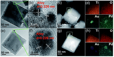 | ||
| Fig. 5 Detailed morphology and composition analysis of two representative samples: (a–d) CR-Au1Pd1 and (e–h) PD-Au1Pd1. (a and e) TEM images, (b and f) HR-TEM images, (c and g) HAADF-STEM images, and (d and h) corresponding EDX mapping of Ti, O, Au, and Pd, respectively. Adapted with permission from ref. 89. Copyright (2018) Royal Society of Chemistry (RSC). | ||
Similarly, Chen et al.92 used one-step in situ photodeposition to deposit different noble metals such as gold, silver, platinum, and palladium on TiO2 nanocrystals (Fig. 6). The photocatalytic activities of M–TiO2 (M = Au, Ag, Pt, and Pd) samples were evaluated by the photocatalytic selective oxidation of benzyl alcohol. The noble metals were supported on hollow TiO2 nanocrystals via the in situ photodeposition method.
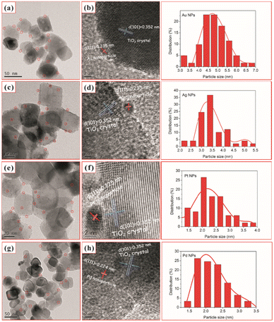 | ||
| Fig. 6 TEM and HRTEM images of TiO2–H after loading with 2 wt% Au (a and b), Ag (c and d), Pt (e and f), and Pd (g and h) and (right) nanoparticle size distribution for the corresponding M–TiO2 (M = Au, Ag, Pt, and Pd). Adapted with permission from ref. 92. Copyright (2017) Elsevier. | ||
Here, the deposition of Au, Ag, Pt, and Pd was achieved using chloroauric acid (HAuCl4), silver nitrate (AgNO3), hexachloroplatinic(IV) acid (H2PtCl6), and palladium(II) chloride (PdCl2) as the precursors, respectively. The TEM and HRTEM image analyses showed 2 wt% of noble NPs loaded on TiO2–H (Fig. 6). The results revealed the presence of spherical noble metal NPs on the surface of the TiO2 support material for different M–TiO2 hybrid nanostructures. As illustrated by the red circles in Fig. 6 (a, c, e, and g), Au, Ag, Pt, and Pd metal NPs were observed as dark spots uniformly decorated on TiO2 nanocrystals. The large conglomerates of metal NPs on TiO2 support were not observed. Notably, the photoreduction of Pt(IV) or Pd(II) ions formed smaller NPs (∼2 nm) as compared to that of the solution consisting of the same amount of Au(III) or Ag(I) ions (NPs ranging from 4 to 5 nm). The larger size of Au NPs, compared to the Pd and Pt NPs, was attributed to a weaker metal support interaction in the case of Au with TiO2. As shown in the HRTEM images in Fig. 6 (b, d, f, and h), characteristic lattice fringes of 0.235, 0.235, 0.225, and 0.224 nm for Au, Ag, Pt, and Pd NPs were observed and indexed to the (111) plane of face-centered cubic structures.
2.2. 1D structures
Lv et al. successively constructed Pt-loaded TiO2 nanotube (TNT) arrays with a uniform distribution of Pt via photodeposition.95Fig. 7 schematically shows the fabrication process of Pt-loaded TiO2 nanotubes. First, a TiO2 nanotube array was produced by the well-known anodization process. A Ti foil was used as an anode, and it was oxidized in an electrolyte solution at 40 V for 8 h against a graphite cathode. The anodic oxidation of Ti led to the formation of TiO2 nanotube arrays.
 | ||
| Fig. 7 Schematic of the fabrication process of Pt/TiO2 NTAs. Adapted with permission from ref. 95. Copyright (2019) Elsevier. | ||
In the following step, photodeposition of Pt on the TiO2 nanotubes was performed using aqueous solutions of H2PtCl6 with different concentrations and illuminating the submerged nanotube array sample with a 500 W mercury lamp for 30 minutes. XPS measurements found that the resulting Pt deposits are most likely metallic. Moreover, UV-vis absorption spectra revealed that the highest visible absorption could be achieved at an initial H2PtCl6 precursor concentration of 3 mmol L−1, corresponding to the highest photodegradation rate of methyl orange.
Jia et al. used photodeposition of Ag on TiO2 nanotubes to prepare photocatalysts, which were used for the photoelectrocatalytic reduction of perchlorate under a bias potential and in the presence of the hole scavenger citric acid.96 The TiO2 nanotubes were prepared by an anodization process similar to the method schematically shown in Fig. 8.
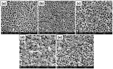 | ||
| Fig. 8 SEM images of (a) TNTs, (b) Ag-TNTs-1, (c) Ag-TNTs-2, (d) Ag-TNTs-3 and used (e) Ag-TNTs-2. Adapted with permission from ref. 96. Copyright (2016) Elsevier. | ||
The Ag loading was carried out by the photoreduction of AgNO3 (volume ratio of ethanol/deionized water equal to 1![[thin space (1/6-em)]](https://www.rsc.org/images/entities/char_2009.gif) :
:![[thin space (1/6-em)]](https://www.rsc.org/images/entities/char_2009.gif) 4) under UV illumination (light of intensity I = 3.5 mW cm2) for 30 minutes with continuous nitrogen purging. SEM images of the resulting photocatalyst are presented in Fig. 8. Bare TiO2 nanotubes are shown in Fig. 8a, and nearly no particles can be seen on their surface. A small number of particles are still present on the surface, which do not belong to Ag (supported by EDX analysis). Fig. 8b–d show the resulting Ag-loaded TiO2 nanotubes for 1, 2, and 3 g L−1 concentrations of initial AgNO3, respectively. It was observed that the number of particles on the TiO2 nanotubes increased with increasing AgNO3 concentration. It was also noted that the average particle size increased with the increase in AgNO3 concentration from 9 nm to 20 nm and to 130 nm, respectively. From photoelectrocatalytic experiments, it was found that the sample shown in Fig. 8c, which was prepared with a 2 g L−1 AgNO3 solution and showing a 0.84% Ag/TiO2 mass ratio, exhibits the highest perchlorate reduction rate.96
4) under UV illumination (light of intensity I = 3.5 mW cm2) for 30 minutes with continuous nitrogen purging. SEM images of the resulting photocatalyst are presented in Fig. 8. Bare TiO2 nanotubes are shown in Fig. 8a, and nearly no particles can be seen on their surface. A small number of particles are still present on the surface, which do not belong to Ag (supported by EDX analysis). Fig. 8b–d show the resulting Ag-loaded TiO2 nanotubes for 1, 2, and 3 g L−1 concentrations of initial AgNO3, respectively. It was observed that the number of particles on the TiO2 nanotubes increased with increasing AgNO3 concentration. It was also noted that the average particle size increased with the increase in AgNO3 concentration from 9 nm to 20 nm and to 130 nm, respectively. From photoelectrocatalytic experiments, it was found that the sample shown in Fig. 8c, which was prepared with a 2 g L−1 AgNO3 solution and showing a 0.84% Ag/TiO2 mass ratio, exhibits the highest perchlorate reduction rate.96
Ren and Liu loaded PdAu alloyed NPs on TiO2 nanowires via a one-step photochemical deposition method, and the Pd/Au ratio in alloyed NPs could be adjusted by changing the Pd2+/Au3+ ratio.101 Reductants and surfactants were avoided in the whole synthesis process. To synthesize PdAu alloyed NPs with different Pd/Au ratios, 16 mL of PdCl2 (0.5 mM) solution in ethanol was mixed with a certain amount of HAuCl4 (10 mM) solution in ethanol. For comparison, the same procedure was modified to deposit Pd or Au NPs on TiO2 nanowires with 0.5 mM PdCl2 or HAuCl4 solution, respectively. After 24 h of hydrothermal growth, TiO2 nanowires were densely distributed on the Ti foil. One single nanowire marked with the red arrow line was selected to estimate its length. Although its two ends exceed the measurement region, its length still reached 15 μm. As shown in the bottom-left inset in Fig. 9a, after UV irradiation for 30 min in PdCl2 solution, the color of the TiO2 nanowire film changed from milky white to black, which indicated the successful loading of Pd NPs on the TiO2 surface. As shown in Fig. 9a, a large amount of Pd NPs was loaded on the TiO2 surface, and the majority was 35–65 nm in diameter. A magnified SEM picture of a few Pd NPs indicated that a single nanoparticle on the nanowire comprised an agglomerate of many smaller NPs, as shown in the upper-left inset in Fig. 9a.
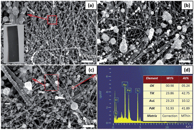 | ||
| Fig. 9 SEM pictures of (a) Pd@TiO2, (b) Au@TiO2 and (c) Pd4Au@TiO2. (d) The EDS spectrum for the particle in panel (c) marked with a red “+” symbol. The upper-left and bottom-left insets in panel (a) are the enlarged SEM image of a few NPs and the photograph of Pd@TiO2, respectively. The inset in panel (c) is the enlarged SEM image for the marked region with a red box. The inset in panel (d) lists the elemental distribution in Pd4Au@TiO2. Adapted with permission from ref. 101. Copyright (2016) Royal Society of Chemistry (RSC). | ||
When HAuCl4 solution was used to deposit Au NPs under identical conditions, the as-synthesized Au nanostructures exhibited a lower density and wider size distribution than Pd NPs loaded NWs (Fig. 9b). It should be noted that their size obviously decreases along with the loading site changing from upper TiO2 nanowires to bottom ones. The mixed solution of PdCl2 and HAuCl4 was used to synthesize PdAu alloyed NPs on TiO2 nanowires. Fig. 9c shows the Pd4Au alloyed NPs synthesized with a Pd2+/Au3+ = 4 ratio in precursor solutions. Except for a few NPs with a diameter of about 100 nm, a large number of smaller NPs were loaded on the TiO2 surface, as shown in the inset in Fig. 9c. Fig. 9d shows the corresponding energy dispersive spectroscopy (EDS) spectrum of the single particle marked with the “+” symbol in Fig. 9c. Among the four elements, the O and Ti elements came from the TiO2 substrate, and Pd and Au came from the photodeposited NPs. The Pd/Au ratio in alloyed NPs was 4.14, which is almost the same as the Pd2+/Au3+ ratio in the precursor solution.
Park et al. demonstrated the development of Au-NP decorated ZnO–TiO2 core–shell NWs via a two-step process; the preparation of ZnO–TiO2 core–shell NWs was carried out using chemical vapor deposition (CVD), and decoration of Au-NPs was done on the ZnO–TiO2 core–shell NWs using photodeposition (PD).102 A schematic representation of ZnO, ZT, and ZTA NWs heterostructure synthesis is shown in Fig. 10. Primarily, a thin layer of carbon was coated on a Si-wafer. Then, well-aligned ZnO NWs were grown on the carbon-coated Si-wafer. Subsequently, a thin layer of TiO2 shell was deposited on the ZnO NWs core. Finally, Au-NPs were decorated on the ZnO–TiO2 core–shell NWs heterostructure by the PD method. It was observed that decoration of plasmonic Au-NPs enhanced the photocurrent density and photoconversion efficiency of as-prepared ZnO–TiO2 core–shell NWs due to increased visible light absorption, efficient electron extraction from Au-NPs due to the Schottky barrier, effective charge separation at multi-interface and transportation through 1D NWs. This study demonstrates that the plasmonic Au-NPs decorated on the ZnO–TiO2 core–shell NWs improve the PEC performance.
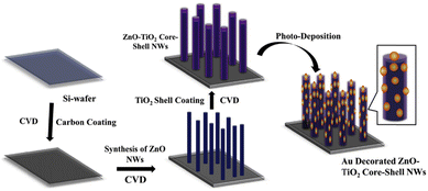 | ||
| Fig. 10 Schematic representation of development of Au-NP decorated ZnO–TiO2 core–shell NWs on the Si-wafer. Adapted with permission from ref. 102 Copyright (2018) American Chemical Society (ACS). | ||
2.3. 2D structures
Alternatively, sputtering and evaporation techniques have been developed to produce columnar or sculptured thin films with enhanced porosity.110 Suzuki et al. reported that surface reaction enhanced the efficiency of obliquely deposited TiO2 thin films with different columnar geometrical shapes, including zigzag, cylindrical, and helical morphologies.117 More so, Goossens et al. reported a fractal (‘forest-like”) 3D TiO2 thin film.118 The choice of deposition method not only plays a role in the thin film structure but is also a contributing factor to the photocatalytic activity of the thin film.119 Another approach to enhance the photocatalytic activity of TiO2 thin films is the decoration by metallic nanostructures via photodeposition. The decoration of TiO2 thin films with noble metals such as Au, Ag, Pd, and Pt has been shown to exhibit excellent absorption properties due to the local surface plasmon resonance (LSPR) activities.120 Using Au and Ag for decorating TiO2 thin films has led to red-shifted and increased LSPR, which reduces charge recombination at the surface of TiO2, yielding an improved overall photocatalytic performance. Furthermore, those metal clusters are also electron acceptors and enhance charge separation, and there can be competing processes.
Tossi et al.121 explained the photodeposition of Pt NPs on TiO2 thin films that were grown via ALD (Fig. 11a). They mainly reported that the photodeposition parameters influence the control and prediction of the deposited nanoparticles' size, density, and loading. Fig. 11c summarizes the SEM images of different samples under different reaction conditions. On the top, the TiO2 deposited FTO-coated glass, samples 5 (see the corresponding parameters in Fig. 11b) and 8 (see the corresponding parameters in Fig. 11b) after the platinum photodeposition are shown with white parts as NPs. On the bottom, three SEM images of sample 7 (see the corresponding parameters in Fig. 11b) are given. They indicated that platinum oxide is visible even at low magnifications, and only a few metallic particles are visible at higher magnifications, which is a characteristic of platinum oxide. This work analyzed the photodeposition method for metal NPs from liquid precursors on ALD-grown films.
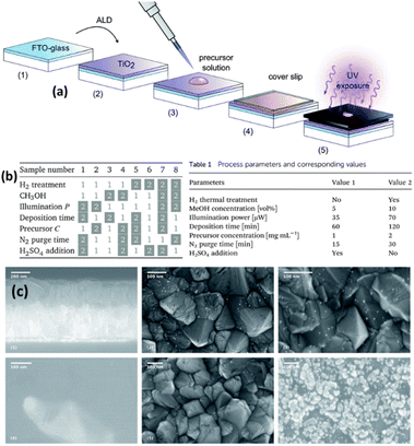 | ||
| Fig. 11 (a) Sample preparation and exposure: the H2 thermal treatment, when applied, takes place between steps (2) and (3). The illuminated area of the sample is 0.15 cm2 out of 5.5 cm2. (b) The eight combinations of parameters for each sample: the white boxes refer to value 1 in Table 1 (inset), while the gray boxes refer to value 2. (c) SEM micrographs: on the top, from left to right, are the section of the FTO-coated glass after the TiO2 deposition, and the surfaces of samples 5 and 8 after the platinum photodeposition, the nanoparticles shown in white. On the bottom part of the figure, three micrographs of sample 7 show the clear-colored platinum oxide well visible already at low magnification and higher magnifications of the darker area, where a few metallic particles are visible, and of the clear area, with the characteristic growth patterns for platinum oxide. Adapted with permission from ref. 121 (2019) Royal Society of Chemistry (RSC). | ||
Recently, a highly active Au nanocluster (NC) fabrication on a TiO2 thin film surface by the photodeposition method was demonstrated.122 The surface coverage of TiO2 by Au NCs was found to be controlled by changing the solvent type and the illumination time. Higher photocatalytic performance was observed at a low surface coverage due to the high optical absorption of TiO2 at UV wavelengths. As indicated in morphological analysis (HIM images in Fig. 12a–d), different solvents (acetone, isopropanol, and 1-hexanol) were investigated to obtain the impacts on the photocatalytic depositions of Au NCs on TiO2. It was observed that water, among the other solvents, resulted in the lowest surface coverage value by Au NCs on TiO2 films. In contrast, the highest density of Au nanoclusters was achieved by a mixture of 1-hexanol–water as a solvent, as illustrated in Fig. 12e.
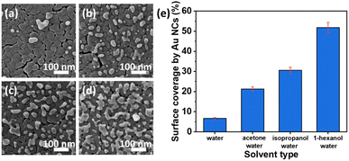 | ||
| Fig. 12 HIM images of Au NCs deposited onto TiO2 in (a) water, (b) acetone–water (v/v: 20/80), (c) isopropanol–water (v/v: 20/80), and (d) 1-hexanol–water (v/v: 20/80) mixtures. (e) Surface coverage (%) by Au NCs deposited with different solvents. Adapted with permission from ref. 122. Copyright (2020) American Chemical Society (ACS). | ||
As mentioned in the previous sections, the photocatalytic deposition method gives strong adhesion between deposited noble metals and the semiconductor surface. It is essential to use these hybrid nanostructures for various applications, especially for continuous water systems. The photocatalytic deposition approach can also pattern micro-/nanostructures without any stabilizer or surfactant, as shown in Fig. 13.20Fig. 13a illustrates the photocatalytic deposition of hierarchical Au needle clusters (HAuNCs) on a highly active TiO2 thin film surface. The non-contact polymer mask is located between the UV LED and the thin film sample. The TiO2 thin film surface can be selectively illuminated to reduce Au ions as metallic Au in only these illuminated areas (Fig. 13b and c). The rest remains empty due to UV LED non-illumination. The photocatalytic deposition approach is practical for preparing various shapes and patterned noble metal structures on semiconductors for well-desired applications (catalysis, plasmonic, and biomedical technologies).
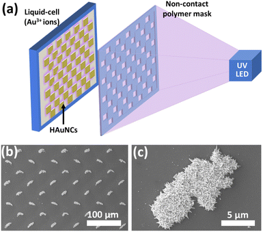 | ||
| Fig. 13 (a) Schematic representation of photocatalytic patterning of the TiO2 thin film with HAuNCs using a noncontact polymer mask. SEM images of (b) periodic HAuNC arrays and (c) a single HAuNC. Adapted with permission from ref. 20. Copyright (2018) Wiley. | ||
3 Concluding remarks and future perspectives of photocatalytic deposition
In recent years, extensive research on noble metal–TiO2 nanostructures has demonstrated their crucial role in various applications such as water splitting, self-cleaning, CO2 reduction, and water remediation. The structure of the noble metal–TiO2 composite is critical in determining its photocatalytic properties. Various studies in the literature on preparing noble metals with different shapes and sizes exist. However, obtaining good adhesion between the noble metal and TiO2 surface is still challenging. Photodeposition is a promising approach to obtain well-desired noble metal structures on TiO2 surfaces with strong adhesion. Noble metal NPs can be quickly grown on the TiO2 surface under light exposure. However, numerous parameters (pH, temperature, precursor, electron sacrificial agent, etc.) affect the size and distribution of the deposited particles. In addition to these parameters, the interaction between solution and OD, 1D, and 2D morphologies might differ due to surface tension forces, drastically affecting the uniformity of the deposited metal nanostructures. This review focused on a few significant types of TiO2 morphologies (0D: NPs and nanocrystals; 1D: nanotubes and nanowires; and 2D: thin films) to better understand the photocatalytic deposition process. Based on available data, more fundamental research on different TiO2 morphologies is still needed to develop highly active photocatalytic structures for specific applications. Hopefully, this review can inspire multidisciplinary research interest in precisely tailoring TiO2 morphology to study in various applications.Data availability
No primary research results, software or code have been included and no new data were generated or analysed as part of this review.Conflicts of interest
There are no conflicts to declare.Acknowledgements
Open access funding enabled and organized by Projekt DEAL.References
- A. P. Alivisatos, Science, 1996, 271, 933–937 CrossRef CAS.
- X. Liu, J. Iocozzia, Y. Wang, X. Cui, Y. Chen, S. Zhao, Z. Li and Z. Lin, Energy Environ. Sci., 2017, 10, 402–434 RSC.
- J. Shondo, S. Veziroglu, T. Tjardts, J. Fiutowski, S. Schröder, Y. K. Mishra, T. Strunskus, H. Rubahn, F. Faupel and O. C. Aktas, Adv. Mater. Interfaces, 2022, 9, 2102126 CrossRef CAS.
- Y. C. Yen, P. H. Chen, J. Z. Chen, J. A. Chen and K. J. Lin, ACS Appl. Mater. Interfaces, 2015, 7, 1892–1898 CrossRef CAS PubMed.
- M. Tomás-Gamasa and J. L. Mascareñas, TiO2-Based Photocatalysis at the Interface with Biology and Biomedicine, ChemBioChem, 2020, 21, 294 CrossRef PubMed.
- S. Liu, M. D. Regulacio, S. Y. Tee, Y. W. Khin, C. P. Teng, L. D. Koh, G. Guan and M. Y. Han, Chem. Rec., 2016, 16, 1965–1990 CrossRef CAS PubMed.
- J. Shondo, S. Veziroglu, T. Tjardts, T. Bin Sarwar, Y. K. Mishra, F. Faupel and O. C. Aktas, Small, 2022, 18, 2203861 CrossRef CAS PubMed.
- K. C. F. Leung, S. Xuan, X. Zhu, D. Wang, C. P. Chak, S. F. Lee, W. K. W. Ho and B. C. T. Chung, Chem. Soc. Rev., 2012, 41, 1911–1928 RSC.
- T. S. Ahmadi, Z. L. Wang, T. C. Green, A. Henglein and M. A. El-Sayed, Science, 1996, 272, 1924–1925 CrossRef CAS PubMed.
- D. Ma, Noble Met. Oxide Hybrid Nanoparticles Fundam. Appl., 2019, pp. 3–6 Search PubMed.
- S. Yoda, K. Ohtake, Y. Takebayashi, T. Sugeta, T. Sako and T. Sato, J. Mater. Chem., 2000, 10, 2151–2156 RSC.
- A. V. Rane, K. Kanny, V. K. Abitha and S. Thomas, Methods for Synthesis of Nanoparticles and Fabrication of Nanocomposites, Elsevier Ltd, 2018 Search PubMed.
- T. Liu, W. Chen, T. Huang, G. Duan, X. Yang and X. Liu, J. Mater. Sci., 2016, 51, 6987–6997 CrossRef CAS.
- J. G. Kang and Y. Sohn, J. Mater. Sci., 2012, 47, 824–832 CrossRef CAS.
- N. P. Dasgupta, C. Liu, S. Andrews, F. B. Prinz and P. Yang, J. Am. Chem. Soc., 2013, 135, 12932–12935 CrossRef CAS PubMed.
- Y. Busby and J. J. Pireaux, J. Electron Spectrosc. Relat. Phenom., 2014, 192, 13–18 CrossRef CAS.
- Annu, A. Ali and S. Ahmed, in Handbook of Ecomaterials, ed. L. M. T. Martínez, O. V. Kharissova and B. I. Kharisov, Springer International Publishing, Cham, 2019, pp. 2281–2325 Search PubMed.
- J. Shondo, S. Veziroglu, D. Stefan, Y. K. Mishra, T. Strunskus, F. Faupel and O. C. Aktas, Appl. Surf. Sci., 2020, 147795 Search PubMed.
- A. Abedini, A. R. Daud, M. Azmi, A. Hamid, N. K. Othman, E. Saion, M. A. A. Hamid, N. K. Othman and E. Saion, Nanoscale Res. Lett., 2013, 8, 1–10 CrossRef PubMed.
- S. Veziroglu, M. Z. Ghori, M. Kamp, L. Kienle, H. G. Rubahn, T. Strunskus, J. Fiutowski, J. Adam, F. Faupel and O. C. Aktas, Adv. Mater. Interfaces, 2018, 5, 1–7 Search PubMed.
- M. Sadowsky and P. D. Payne, J. Electrochem. Soc., 1958, 105, 105 CrossRef.
- J. Ohyama, A. Yamamoto, K. Teramura, T. Shishido and T. Tanaka, ACS Catal., 2011, 1, 187–192 CrossRef CAS.
- K. Wenderich and G. Mul, Chem. Rev., 2016, 116, 14587–14619 CrossRef CAS PubMed.
- M. A. Fox and M. T. Dulay, Chem. Rev., 1993, 93, 341–357 CrossRef CAS.
- O. Carp, C. L. Huisman and A. Reller, Prog. Solid State Chem., 2004, 32, 33–177 CrossRef CAS.
- C. P. C. V. Bernardo, R. A. M. Lameirinhas, J. P. de Melo Cunha and J. P. N. Torres, A Revision of the Semiconductor Theory from History to Applications, Springer International Publishing, 2024, vol. 6 Search PubMed.
- W. Guo, J. Huang and W. D. Wei, in Plasmonic Catalysis, Wiley, 2021, pp. 295–322 Search PubMed.
- W. Schottky, Naturwissenschaften, 1938, 26, 843 CrossRef CAS.
- H. Dong, G. Zeng, L. Tang, C. Fan, C. Zhang, X. He and Y. He, Water Res., 2015, 79, 128–146 CrossRef CAS PubMed.
- G. M. Haselmann and D. Eder, ACS Catal., 2017, 7, 4668–4675 CrossRef CAS.
- L. Kavan, J. Solid State Electrochem., 2024, 28, 829–845 CrossRef CAS.
- V. Mansfeldova, M. Zlamalova, H. Tarabkova, P. Janda, M. Vorokhta, L. Piliai and L. Kavan, J. Phys. Chem. C, 2021, 125, 1902–1912 CrossRef CAS.
- M. Zlamalova, V. Mansfeldova, H. Tarabkova, H. Krysova and L. Kavan, J. Solid State Electrochem., 2023, 27, 1935–1943 CrossRef CAS.
- C. Lattyak, K. Gehrke and M. Vehse, J. Phys. Chem. C, 2022, 126, 13929–13935 CrossRef CAS.
- Q. Huang, T. Gao, F. Niu, D. Chen, Z. Chen, L. Qin, X. Sun, Y. Huang and K. Shu, Superlattices Microstruct., 2014, 75, 890–900 CrossRef CAS.
- S. Garcia-Segura and E. Brillas, J. Photochem. Photobiol., C, 2017, 31, 1–35 CrossRef CAS.
- F. O. F. Business, A. Arts, G. Chidichimo, L. Filippelli, E. L. Pierre, B. Zhou, B. Shi, D. Jin, X. Liu, F. Jiang, W. C. H. Choy, X. Li, D. Zhang, J. Cheng, A. K. Gaharwar, N. A. Peppas, A. Khademhosseini, A. Nouioua, D. Barkat, M. L. Petrus, J. Schlipf, C. Li, T. P. Gujar, N. Giesbrecht, P. Müller-Buschbaum, M. Thelakkat, T. Bein, S. Hüttner, P. Docampo, L. Shaabani, R. Singh, S. Dutta, A. Tampieri, G. Celotti, E. Landi, C. A. Mirkin, R. L. Letsinger, R. C. Mucic and J. J. Storhoff, Fuel, 2015, 111, 607–620 Search PubMed.
- S. M. Gupta and M. Tripathi, Chin. Sci. Bull., 2011, 56, 1639–1657 CrossRef CAS.
- A. Vahl, S. Veziroglu, B. Henkel, T. Strunskus, O. Polonskyi, O. C. Aktas and F. Faupel, Materials, 2019, 12, 2840 CrossRef CAS PubMed.
- S. Veziroglu, J. Hwang, J. Drewes, I. Barg, J. Shondo, T. Strunskus, O. Polonskyi, F. Faupel and O. C. Aktas, Mater. Today Chem., 2020, 16, 100251 CrossRef CAS.
- S. Kalantzis, S. Veziroglu, T. Kohlhaas, C. Flörke, Y. K. Mishra, J. Wiltfang, Y. Açil, F. Faupel, O. C. Aktas and A. Gülses, RSC Adv., 2020, 10, 28935–28940 RSC.
- C. Renz, Helv. Chim. Acta, 1921, 4, 961–968 CrossRef CAS.
- C. Renz, Helv. Chim. Acta, 1932, 15, 1077–1084 CrossRef CAS.
- W. C. Clark and A. G. Vondjidis, J. Catal., 1965, 4, 691–696 CrossRef CAS.
- B. Kraeutler and A. J. Bard, J. Am. Chem. Soc., 1978, 100, 4317–4318 CrossRef CAS.
- S. Dadsetan, S. Baghshahi and S. M. M. Hadavi, J. Australas. Ceram. Soc., 2018, 54, 383–388 CrossRef CAS.
- F. Zhang, J. Chen, X. Zhang, W. Gao, R. Jin, N. Guan and Y. Li, Langmuir, 2004, 20, 9329–9334 CrossRef CAS.
- J. M. Herrmann, J. Disdier and P. Pichat, J. Phys. Chem., 1986, 90, 6028–6034 CrossRef CAS.
- N. A. Jani, C. Haw, W. Chiu, S. A. Rahman, P. Khiew, Y. Lim, R. Abd-Shukor and M. A. A. Hamid, J. Nanomater., 2020, 2020, 1–11 CrossRef.
- E. M. See, C. Tossi, L. Hällström and I. Tittonen, ACS Omega, 2020, 5, 10671–10679 CrossRef CAS PubMed.
- M. C. Hidalgo, J. J. Murcia, J. A. Navío and G. Colón, Appl. Catal., A, 2011, 397, 112–120 CrossRef CAS.
- L. G. Devi and R. Kavitha, Appl. Surf. Sci., 2016, 360, 601–622 CrossRef.
- A. Hammad, A. Anzai, X. Zhu, A. Yamamoto, D. Ootsuki, T. Yoshida, A. EL-Shazly, M. Elkady and H. Yoshida, Catal. Lett., 2020, 150, 1081–1088 CrossRef CAS.
- D. Ferrah and P. Tieu, ACS Appl. Nano Mater., 2020, 3, 5855–5861 CrossRef CAS.
- Y. J. Hwang, C. Hahn, B. Liu and P. Yang, ACS Nano, 2012, 6, 5060–5069 CrossRef CAS.
- F. Sieland, J. Schneider and D. W. Bahnemann, Phys. Chem. Chem. Phys., 2018, 20, 8119–8132 RSC.
- J. Taing, M. H. Cheng and J. C. Hemminger, ACS Nano, 2011, 5, 6325–6333 CrossRef CAS PubMed.
- S. Bhardwaj, D. Sharma, P. Kumari and B. Pal, Opt. Mater., 2020, 106, 109975 CrossRef CAS.
- Y. Lee, E. Kim, Y. Park, J. Kim, W. H. Ryu, J. Rho and K. Kim, J. Mater., 2018, 4, 83–94 Search PubMed.
- B. Gupta, A. A. Melvin, T. Matthews, S. Dash and A. K. Tyagi, Renewable Sustainable Energy Rev., 2016, 58, 1366–1375 CrossRef CAS.
- C. Wang, H. Liu, Y. Liu, G. He and C. Jiang, Appl. Surf. Sci., 2014, 319, 2–7 CrossRef CAS.
- T. Ohno, K. Sarukawa, K. Tokieda and M. Matsumura, J. Catal., 2001, 203, 82–86 CrossRef CAS.
- B. Ohtani, O. O. Prieto-Mahaney, D. Li and R. Abe, J. Photochem., Photobiol. A, 2010, 216(2–3), 179–182 CrossRef CAS.
- R. I. Bickley, T. Gonzalez-Carreno, J. S. Lees, L. Palmisano and R. J. D. Tilley, J. Solid State Chem., 1991, 92, 178–190 CrossRef CAS.
- B. Ohtani, O. O. Prieto-Mahaney, D. Li and R. Abe, J. Photochem. Photobiol., A, 2010, 216, 179–182 CrossRef CAS.
- Z. Jiang, Z. Y. Zhang, W. Shangguan, M. A. Isaacs, L. J. Durndell, C. M. A. Parlett and A. F. Lee, Catal. Sci. Technol., 2016, 6, 81–88 RSC.
- A. Tanaka, K. Teramura, S. Hosokawa, H. Kominami and T. Tanaka, Chem. Sci., 2017, 8, 2574–2580 RSC.
- S. Dadsetan, S. Baghshahi, F. Farshidfar and S. M. M. Hadavi, Ceram. Int., 2017, 43, 9322–9326 CrossRef CAS.
- A. Sclafani and J. M. Herrmann, J. Photochem. Photobiol., A, 1998, 113, 181–188 CrossRef CAS.
- J. Ma, X. Guo, Y. Zhang and H. Ge, Chem. Eng. J., 2014, 258, 247–253 CrossRef CAS.
- E. T. Wahyuni, R. Roto, D. Novarita, K. P. Suwondo and B. Kuswandi, J. Environ. Chem. Eng., 2019, 7, 103178 CrossRef CAS.
- J. C. Colmenares, P. Lisowski, D. Łomot, O. Chernyayeva and D. Lisovytskiy, ChemSusChem, 2015, 8, 1676–1685 CrossRef CAS PubMed.
- L. Galeano, S. Valencia, J. M. Marín, G. Restrepo, J. A. Navío and M. C. Hidalgo, Mater. Res. Express, 2019, 6, 1050d9 CrossRef CAS.
- V. P. Chavda, in Applications of Targeted Nano Drugs and Delivery Systems, Elsevier, 2019, pp. 69–92 Search PubMed.
- B. Dubertret, Science, 2002, 298, 1759–1762 CrossRef CAS PubMed.
- X. Gao, Y. Cui, R. M. Levenson, L. W. K. Chung and S. Nie, Nat. Biotechnol., 2004, 22, 969–976 CrossRef CAS PubMed.
- O. D'Hennezel and D. F. Ollis, Helv. Chim. Acta, 2001, 84, 3511–3518 CrossRef.
- K. Nagaveni, G. Sivalingam, M. Hegde and G. Madras, Appl. Catal., B, 2004, 48, 83–93 CrossRef CAS.
- M. Lazzeri, A. Vittadini and A. Selloni, Phys. Rev. B: Condens. Matter Mater. Phys., 2001, 63, 155409 CrossRef.
- S. S. El-Deen, A. M. Hashem, A. E. Abdel Ghany, S. Indris, H. Ehrenberg, A. Mauger and C. M. Julien, Ionics, 2018, 24, 2925–2934 CrossRef CAS.
- Y. T. Kim, Y. S. Park, H. Myung and H. K. Chae, Colloids Surf., A, 2008, 313–314, 260–263 CrossRef.
- B. K. Mutuma, G. N. Shao, W. D. Kim and H. T. Kim, J. Colloid Interface Sci., 2015, 442, 1–7 CrossRef CAS PubMed.
- Y. Yao, T. Zhai, C. Liu, Y. Guan, J. Zhang, D. Xu and J. Luo, Ceram. Int., 2015, 41, 14740–14747 CrossRef CAS.
- M. H. Nateq and R. Ceccato, Adv. Mater. Sci. Eng., 2019, 2019, 1–14 CrossRef.
- F. Wang, Z. Shi, F. Gong, J. Jiu and M. Adachi, Chin. J. Chem. Eng., 2007, 15, 754–759 CrossRef CAS.
- F. Sayilkan, M. Asiltürk, H. Sayilkan, Y. Önal, M. Akarsu and E. Arpaç, Turk. J. Chem., 2005, 29, 697–706 CAS.
- S. Mathew, A. Kumar Prasad, T. Benoy, P. P. Rakesh, M. Hari, T. M. Libish, P. Radhakrishnan, V. P. N. Nampoori and C. P. G. Vallabhan, J. Fluoresc., 2012, 22, 1563–1569 CrossRef CAS PubMed.
- C. Liu, X. Han, S. Xie, Q. Kuang, X. Wang, M. Jin, Z. Xie and L. Zheng, Chem.–Asian J., 2013, 8, 282–289 CrossRef CAS PubMed.
- Q. Chen, X. Chen, M. Fang, J. Chen, Y. Li, Z. Xie, Q. Kuang and L. Zheng, J. Mater. Chem. A, 2019, 7, 1334–1340 RSC.
- X. Chen, Z. Cai, X. Chen and M. Oyama, J. Mater. Chem. A, 2014, 2, 5668–5674 RSC.
- Z.-L. Wang, J.-M. Yan, Y.-F. Zhang, Y. Ping, H.-L. Wang and Q. Jiang, Nanoscale, 2014, 6, 3073 RSC.
- Y. Chen, Y. Wang, W. Li, Q. Yang, Q. Hou, L. Wei, L. Liu, F. Huang and M. Ju, Appl. Catal., B, 2017, 210, 352–367 CrossRef CAS.
- I. Paramasivam, H. Jha, N. Liu and P. Schmuki, Small, 2012, 8, 3073–3103 CrossRef CAS PubMed.
- V. Zwilling, E. Darque-Ceretti, A. Boutry-Forveille, D. David, M. Y. Perrin and M. Aucouturier, Surf. Interface Anal., 1999, 27, 629–637 CrossRef CAS.
- J. Lv, H. Gao, H. Wang, X. Lu, G. Xu, D. Wang, Z. Chen, X. Zhang, Z. Zheng and Y. Wu, Appl. Surf. Sci., 2015, 351, 225–231 CrossRef CAS.
- Y. Jia, L. Ye, X. Kang, H. You, S. Wang and J. Yao, J. Photochem. Photobiol., A, 2016, 328, 225–232 CrossRef CAS.
- B. Li, J.-M. Wu, T.-T. Guo, M.-Z. Tang and W. Wen, Nanoscale, 2014, 6, 3046 RSC.
- I. S. Grover, R. C. Prajapat, S. Singh and B. Pal, Sol. Energy, 2017, 144, 612–618 CrossRef CAS.
- C. Wang, L. Yin, L. Zhang, N. Liu, N. Lun and Y. Qi, ACS Appl. Mater. Interfaces, 2010, 2, 3373–3377 CrossRef CAS PubMed.
- S. S. Mandal and A. J. Bhattacharyya, Talanta, 2010, 82, 876–884 CrossRef CAS PubMed.
- S. Ren and W. Liu, J. Mater. Chem. A, 2016, 4, 2236–2245 RSC.
- J. Park, P. R. Deshmukh, Y. Sohn and W. G. Shin, J. Alloys Compd., 2019, 787, 1310–1319 CrossRef CAS.
- T. Ohno, S. Y. Lee and Y. Yang, Rare Met., 2015, 34, 291–300 CrossRef CAS.
- E. Bae, N. Murakami and T. Ohno, J. Mol. Catal. A: Chem., 2009, 300, 72–79 CrossRef CAS.
- T. Ohno, T. Higo, H. Saito, S. Yuajn, Z. Jin, Y. Yang and T. Tsubota, J. Mol. Catal. A: Chem., 2015, 396, 261–267 CrossRef CAS.
- T. Ohno, K. Sarukawa and M. Matsumura, New J. Chem., 2002, 26, 1167–1170 RSC.
- D. Chen, Y. Cheng, N. Zhou, P. Chen, Y. Wang, K. Li, S. Huo, P. Cheng, P. Peng, R. Zhang, L. Wang, H. Liu, Y. Liu and R. Ruan, J. Cleaner Prod., 2020, 268, 121725 CrossRef CAS.
- D. Li, H. Haneda, S. Hishita and N. Ohashi, Chem. Mater., 2005, 17, 2596–2602 CrossRef CAS.
- J. Rodríguez, M. Gómez, J. Lu, E. Olsson and C. G. Granqvist, Adv. Mater., 2000, 12, 341–343 CrossRef.
- M. Z. Ghori, S. Veziroglu, B. Henkel, A. Vahl, O. Polonskyi, T. Strunskus, F. Faupel and O. C. Aktas, Sol. Energy Mater. Sol. Cells, 2018, 178, 170–178 CrossRef CAS.
- V. G. Bessergenev, R. J. F. Pereira, M. C. Mateus, I. V. Khmelinskii, D. A. Vasconcelos, R. Nicula, E. Burkel, A. M. Botelho Do Rego and A. I. Saprykin, Thin Solid Films, 2006, 503, 29–39 CrossRef CAS.
- J. Yu, X. Zhao and Q. Zhao, Thin Solid Films, 2000, 379, 7–14 CrossRef CAS.
- Y. G. Seo, M. A. Kim, H. Lee and W. Lee, Sol. Energy Mater. Sol. Cells, 2011, 95, 332–335 CrossRef CAS.
- A. Ranga Rao and V. Dutta, Sol. Energy Mater. Sol. Cells, 2007, 91, 1075–1080 CrossRef CAS.
- D. Dastan, S. L. Panahi and N. B. Chaure, J. Mater. Sci.: Mater. Electron., 2016, 27, 12291–12296 CrossRef CAS.
- J. G. Yu, H. G. Yu, B. Cheng, X. J. Zhao, J. C. Yu and W. K. Ho, J. Phys. Chem. B, 2003, 107, 13871–13879 CrossRef CAS.
- M. Suzuki, T. Ito and Y. Taga, Appl. Phys. Lett., 2001, 78, 3968–3970 CrossRef CAS.
- A. Goossens, E. L. Maloney and J. Schoonman, Chem. Vap. Deposition, 1998, 4, 109–114 CrossRef CAS.
- B. Henkel, T. Neubert, S. Zabel, C. Lamprecht, C. Selhuber-Unkel, K. Rätzke, T. Strunskus, M. Vergöhl and F. Faupel, Appl. Catal., B, 2016, 180, 362–371 CrossRef CAS.
- S. Veziroglu, M. Ullrich, M. Hussain, J. Drewes, J. Shondo, T. Strunskus, J. Adam, F. Faupel and O. C. Aktas, Surf. Coat. Technol., 2020, 389, 125613 CrossRef CAS.
- C. Tossi, L. Hällström, J. Selin, M. Vaelma, E. See, J. Lahtinen and I. Tittonen, J. Mater. Chem. A, 2019, 7, 14519–14525 RSC.
- S. Veziroglu, A.-L. Obermann, M. Ullrich, M. Hussain, M. Kamp, L. Kienle, T. Leißner, H.-G. Rubahn, O. Polonskyi, T. Strunskus, J. Fiutowski, M. Es-Souni, J. Adam, F. Faupel and O. C. Aktas, ACS Appl. Mater. Interfaces, 2020, 12, 14983–14992 CrossRef CAS PubMed.
| This journal is © The Royal Society of Chemistry 2024 |

