
 Open Access Article
 This Open Access Article is licensed under a Creative Commons Attribution-Non Commercial 3.0 Unported Licence
Vertical heterostructure of graphite–MoS2 for gas sensing†
M.
Tripathi‡
 *a,
G.
Deokar‡
b,
J.
Casanova-Chafer
c,
J.
Jin
b,
A.
Sierra-Castillo
d,
S. P.
Ogilvie
a,
F.
Lee
ae,
S. A.
Iyengar
f,
A.
Biswas
f,
E.
Haye
g,
A.
Genovese
h,
E.
Llobet
c,
J.-F.
Colomer
d,
I.
Jurewicz
i,
V.
Gadhamshetty
*j,
P. M.
Ajayan
f,
Udo
Schwingenschlögl
b,
Pedro M. F. J.
Costa
b and
A. B.
Dalton
*a
*a,
G.
Deokar‡
b,
J.
Casanova-Chafer
c,
J.
Jin
b,
A.
Sierra-Castillo
d,
S. P.
Ogilvie
a,
F.
Lee
ae,
S. A.
Iyengar
f,
A.
Biswas
f,
E.
Haye
g,
A.
Genovese
h,
E.
Llobet
c,
J.-F.
Colomer
d,
I.
Jurewicz
i,
V.
Gadhamshetty
*j,
P. M.
Ajayan
f,
Udo
Schwingenschlögl
b,
Pedro M. F. J.
Costa
b and
A. B.
Dalton
*a
aDepartment of Physics and Astronomy, University of Sussex, Brighton BN1 9RH, UK. E-mail: m.tripathi@sussex.ac.uk; A.B.Dalton@sussex.ac.uk
bKing Abdullah University of Science and Technology (KAUST), Physical Science and Engineering Division, Thuwal, 23955 - 6900, Saudi Arabia
cUniversitat Rovira i Virgili, MINOS, Avda. Països Catalans, 26, 43007 Tarragona, Spain
dResearch Group on Carbon Nanostructures (CARBONNAGe), University of Namur, 5000 Namur, Belgium
eInternational Institute for Nanocomposites Manufacturing (IINM), WMG, University of Warwick, Coventry CV47AL, UK
fDepartment of Materials Science and NanoEngineering, Rice University, Houston, Texas 77005, USA
gLaboratoire d’Analyse par Réactions Nucléaires (LARN), Namur Institute of Structured Matter (NISM), University of Namur, 61 Rue de Bruxelles, 5000 Namur, Belgium
hKing Abdullah University of Science and Technology, Core Labs, Thuwal, 23955-6900, Saudi Arabia
iDepartment of Physics, Faculty of Engineering & Physical Sciences, University of Surrey, Guildford GU2 7XH, UK
jDepartment of Civil and Environmental Engineering, and 2D-Materials for Biofilm Engineering, Science, and Technology Center, South Dakota School of Mines and Technology, Rapid City, SD 57701, USA. E-mail: venkataramana.gadhamshetty@sdsmt.edu
First published on 8th May 2024
Abstract
2D materials, given their form-factor, high surface-to-volume ratio, and chemical functionality have immense use in sensor design. Engineering 2D heterostructures can result in robust combinations of desirable properties but sensor design methodologies require careful considerations about material properties and orientation to maximize sensor response. This study introduces a sensor approach that combines the excellent electrical transport and transduction properties of graphite film with chemical reactivity derived from the edge sites of semiconducting molybdenum disulfide (MoS2) through a two-step chemical vapour deposition method. The resulting vertical heterostructure shows potential for high-performance hybrid chemiresistors for gas sensing. This architecture offers active sensing edge sites across the MoS2 flakes. We detail the growth of vertically oriented MoS2 over a nanoscale graphite film (NGF) cross-section, enhancing the adsorption of analytes such as NO2, NH3, and water vapor. Raman spectroscopy, density functional theory calculations and scanning probe methods elucidate the influence of chemical doping by distinguishing the role of MoS2 edge sites relative to the basal plane. High-resolution imaging techniques confirm the controlled growth of highly crystalline hybrid structures. The MoS2/NGF hybrid structure exhibits exceptional chemiresistive responses at both room and elevated temperatures compared to bare graphitic layers. Quantitative analysis reveals that the sensitivity of this hybrid sensor surpasses other 2D material hybrids, particularly in parts per billion concentrations.
New conceptsOur work presents an innovative design that comprises a unique stacking arrangement of heterolayers of 2D materials: molybdenum sulfide over graphitic layers. The vertically oriented molybdenum sulfide's (MoS2's) edge sites serve as receptors for gaseous analytes, ensuring selectivity, while horizontally placed graphene acts as the conductive medium for enhanced sensing performance. This architecture creates next-generation chemiresistors with superior performance achieved through synergy between hetero-atoms of 2D materials. The study further unravels atomic-scale resolution and deciphers the selectivity mechanism towards oxidizing and reducing gases in dry and humid conditions. This is the first report in the literature demonstrating the potential of vertical heterostructure as a gas sensor. These findings bridge the key knowledge gap of heterointerfaces between 2D materials, extending beyond graphitic carbon sheets. We believe our results will capture the attention of a broad audience, specifically the researchers interested in the nanoscience of 2D materials, heterostructures and gas sensors. This work will interest scientists and practitioners interested in utilizing 2D materials for selecting and targeting sensing in diverse domains, including healthcare. |
Introduction
Environmental pollutants are a major concern for air quality, often associated with industrial and transport emissions, with significant consequences for public and individual health.1 Nearly 4.2 million premature mortalities are reported annually due to direct results from exposure to air pollutants, including oxides of nitrogen, sulfur and carbon.2 This has driven demand for gas sensing devices for domestic and public spaces, industrial and transportation environments, for the detection of toxic domestic gases and environmental monitoring.3 To this end, intensive research has fulfilled the global need for cost-effective, highly sensitive, and miniaturised gas sensors that can detect adsorbed analytes with efficient response and recovery time. Traditional approaches for gas sensing include metal oxide semiconductors, which have been implemented for commercial applications.4 Nevertheless, several drawbacks remain, including high operating temperature (>200 °C), degradation of the sensitivity and stability of the sensor owing to variation in the microstructure of the metal oxide at high temperatures, significant baseline drift, poor selectivity, and the strong influence of humidity.52D materials have proven to be an alternative for chemiresistive gas sensors. They can be fabricated in inexpensive devices with minimal power consumption, extreme flexibility, and portability.6 Transition metal dichalcogenides (TMDs) have attracted huge interest in gas sensing due to their unique electronic and chemical functionalisation.7–11 Among the TMDs, molybdenum disulfide (MoS2) has been widely studied as a multi-functional material due to its tuneable properties in electronics and sensors.12–17 MoS2 sheets grown by chemical vapor deposition (CVD) with a controlled number of layers, sizes, and arbitrary shapes, for instance, nanoplates, nanorods, nanoflowers, etc. have been reported.8,16–21 This has led the recent development of heterostructures of MoS2 along with other layered materials (e.g., MoS2/graphene,22,23 MoS2/WS2,24 MoS2/CdSe,25etc.). Among them, heterostructures of MoS2/graphitic carbon are particularly fascinating due to outstanding properties arising from the van der Waals interfaces,26–29i.e., without chemical alteration at the interface that could influence the transport properties. These ultrathin MoS2 structures with abundant active edge sites coupled to graphitic carbon support are extremely useful in enhancing the device performance in sensing, catalysis, and battery applications.26,30 MoS2 flakes on carbon-based materials present a complementary architecture where individual layers contribute to each other as chemically active and electrically conductive, respectively.31 A wide range of applications have been demonstrated where MoS2 is grown/transferred on conducting substrate for electronics and electrocatalysis.17,32,33 Nevertheless, heterostructures comprising MoS2 and graphitic carbon as chemiresistors remain relatively unexplored, and comprehensive studies are needed in this direction.
In the present work, a heterostructure of vertically grown MoS2 on horizontal NGF is demonstrated as a chemiresistor for gas sensing applications, where the edges of semiconducting MoS2 promote adsorption of analyte gases (NO2, NH3), while graphene as a conducting transducer. The preparation of the hybrid architecture comprises a two-step CVD process with careful control over the growth to yield centimetre-scale heterostructure films. Surface analysis techniques have been implemented to reveal the morphology of atomically resolved edge atoms of the hybrid structure with potential lattice planes at the graphene–MoS2 interface. Real-time gas sensing response has been demonstrated in different conditions: ambient, humid and moderately elevated temperatures (150 °C). The doping mechanism is interpreted through Raman spectroscopy with the aid of Kelvin probe surface potential maps and corroborated through density functional theory simulation. This hybrid structure of MoS2/NGF demonstrates the synergy between the two different systems for sensitivity as well as selectivity of chemical and gas detection. This design of hybrid structures will be useful for detecting a broad range of analytes in extremely low concentrations of parts per billion (ppb) and for developing sensitive and portable chemiresistors.
Results and discussion
The atomic scale structure of the hybrid architecture of MoS2 on graphene is illustrated in Fig. 1a, where vertically aligned MoS2 sheets are grown over NGF. The preparation of the hybrid structures through various processing steps is described in detail in Fig. S1 (ESI†). The MoS2 and NGF sheets were grown on Si/SiO2 (oxide thickness 300 nm), with the elemental composition of the MoS2/NGF/SiO2/Si structure shown in Fig. S2 (ESI†) and its vertically aligned architecture over a horizontally stacked and wrinkled graphite sheet in Fig. S3 (ESI†). In this heterostructure, the edge atoms of semiconducting MoS2 flakes are exposed to the local environment and connected to the conducting network of graphite layers, which leads to adsorption, enhanced charge transfer and sensitivity of the device.30 The scanning electron microscopy (SEM) images in Fig. 1b of the cross-section view of the hybrid structure clearly distinguish between NGF (thickness between horizontal red color dashed line) and MoS2 layer (thickness between horizontal yellow line). The top view of the heterostructure reveals densely packed MoS2 grains over the basal plane and wrinkled regions that retain the NGF topographical feature (Fig. 1c). The height distribution of the MoS2 flakes over graphene is illustrated through an AFM image and line profile (inset) in Fig. 1d, revealing size variation from 5 to 20 nm. Close observation reveals that the granular-shaped MoS2 flakes are aligned in the vertical direction, corroborated by high-resolution SEM micrographs in Fig. S4 (ESI†). The width of the aligned MoS2 granules plays an essential role in having the appropriate number of edge active sites towards the gaseous analyte and interfacial interaction between MoS2 and carbon atoms for effective charge transfer. Recently, Mao and coworkers demonstrated that too thin or small granules of MoS2 sheets could lead to incomplete crystallization.34 Nevertheless, uncontrolled thickness could lead to continuous layers of MoS2 with fewer dangling edge S atoms that alter its performance and efficiency.30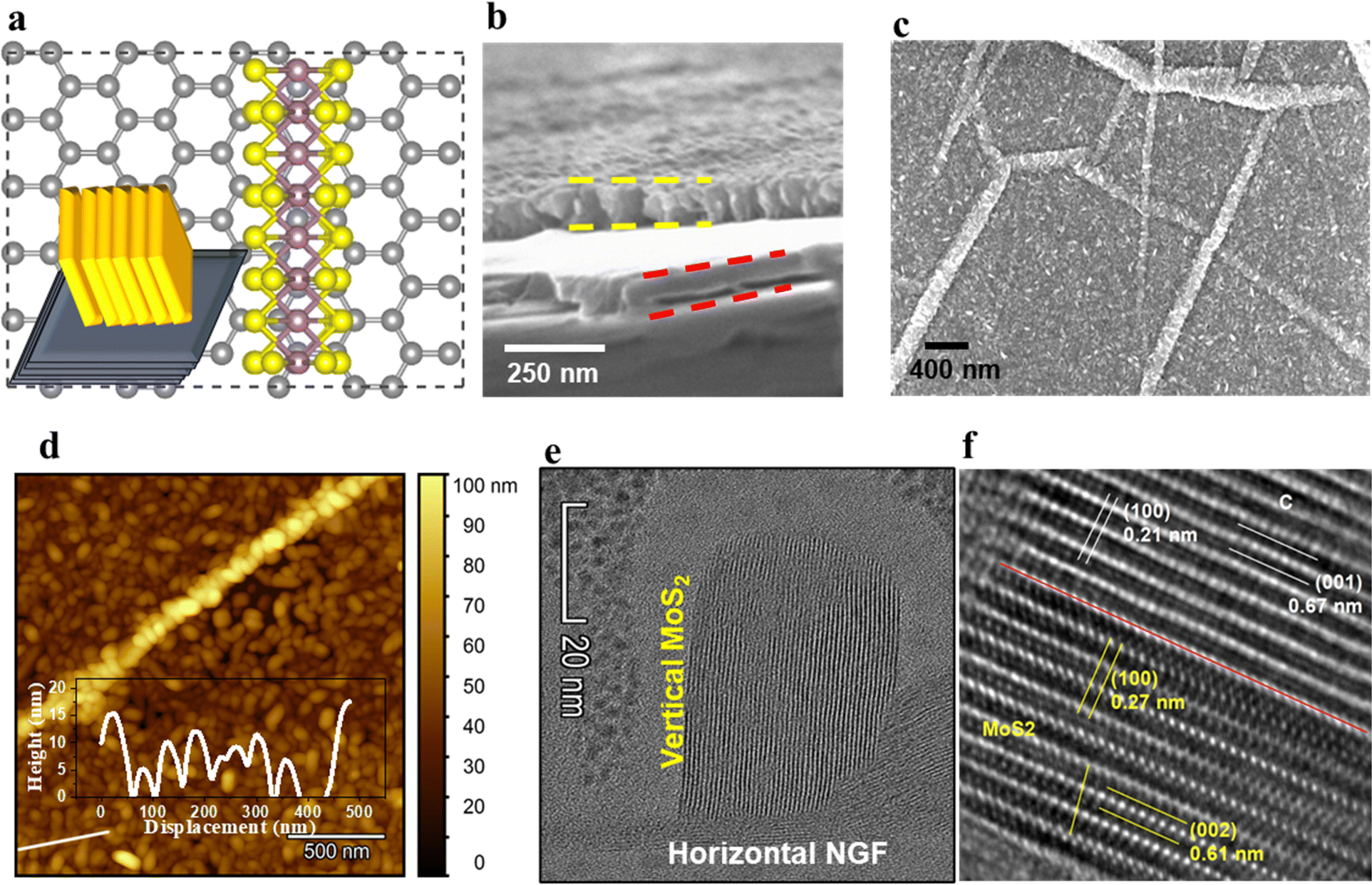 | ||
| Fig. 1 Micro-to-atomic scale visualisation of the hybrid structure. (a) Schematic set-up of vertical hierarchy and simulated atomic arrangement of top view of MoS2/NGF used as a hybrid structure. (b) SEM micrograph of a cross-section revealing the hierarchy of different sheets as MoS2 (region marked with yellow dashed line). (c) Top view SEM micrograph of MoS2/NGF, where grains of MoS2 topping is distributed over different landscapes of NGF. (d) AFM image showing the height variations of MoS2/NGF at different landscapes of edges and basal plane; inset shows the line profile of grain distribution. (e) Nanoscopic resolved TEM images of MoS2 and NGF revealing the vertically aligned MoS2 atoms of graphene layers. (f) The atomically resolved interface between MoS2 and NGF shows the similar basal plane of NGF and MoS2 as (100) close to the interface axis (red colour) and (002) MoS2 plane far from the interface axis. | ||
It is crucial to monitor the crystal planes of the heterostructure to understand the arrangement of edge sulfur atoms in MoS2 grains and their configuration at the interface with the carbon atoms. Therefore, atomic scale lattice planes are analysed through high-resolution transmission electron microscopy (HR-TEM), revealing the MoS2 (100) and (002) lattice planes at 0.27 nm (in-plane S–S separation) and 0.61 nm (out-of-plane sheet separation) respectively, and for the graphite (100) and (002) lattice planes at 0.21 nm (in-plane carbon separation) and 0.335 nm (0.67/2 nm, out-of-plane graphene sheet separation) respectively (Fig. 1e and f). The atomic arrangement at the interface in the hybrid structure reveals epitaxial symmetry between MoS2 and NGF connected through contact planes (002) (Fig. 1f). This epitaxy can be described by the following symmetry relations as NGF [002]//MoS2 [002], NGF [100]//MoS2 [100], NGF b-axis//MoS2b-axis, where the first term represents the planar alignment, the second term is direction alignment of the interface, and the third term is the zone axis alignment. The lattice mismatch (η) between the two crystal structures is defined as the absolute difference between two lattice spacings (d1, d2) along a certain crystal direction relative to the average of the lattice spacings given by relation (1):35
 | (1) |
The η values for the corresponding alignments are 58.7% for the planar equation, 24.6%, and 24.9% for the two vector equations, respectively. These findings are consistent with a semi-coherent NGF/MoS2 interface where five NGF (002) lattice units fit four MoS2 (002) lattice units. The attachment of sulfur atoms to central Mo atoms (i.e. S-end) are observed, which could play a pivotal role in detecting gases as unravelled through the density functional theory simulation.
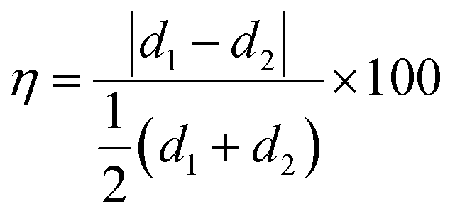
XPS measurement of the hybrid structure reveals the elemental composition as well as the oxidation state of Mo. The NGF/SiO2/Si configuration without MoS2 sheet shows an asymmetric peak centred at 284.9 eV of C 1s core level (Fig. 2a), corresponding to graphitic carbon.36 Nevertheless, traces of O content as a contaminant from air exposure have been observed in Fig. 2b. Interestingly, no C signal is detected after the deposition of smaller size Mo film (≈10 nm), indicating complete coverage of Mo films. Here, the O 1s and Mo 3d (Fig. 2b and c) confirm molybdenum oxide formation, with numerous peaks contribution. These contributions are attributed to the multiple spin–orbit doublets of MoO2 (first doublet at 229.5 eV). The traces of Mo oxide phase is verified by a small doublet peak centered at 232.8 eV (Fig. 2c) and at O 1s core-level spectrum at 530.3 eV (Fig. 2b). The presence of MoO3 is also confirmed by peak contributions at 233 eV. The oxidation of sputtered Mo film is recurrent and confirmed on O 1s level, with a major contribution at 530.3 eV corresponding to Mo–O bonds. After sulfurisation, the formation of MoS2 is confirmed at Mo 3d and S 2p core levels (Fig. 2c and d). The Mo signal is composed of a doublet centred at 229.1 eV (marked by a solid blue line) corresponding to Mo4+, while the contribution at 226.2 eV is attributed to S 2s signal. These results are in excellent agreement with the reference literature reporting MoS2 formation.12,37–39 Additionally, the S 2p signal (Fig. 2d) is composed of a single doublet centred at 161.9 eV, further revealing the formation of MoS2.12,15 The Mo![[thin space (1/6-em)]](https://www.rsc.org/images/entities/char_2009.gif) :S ratio of 1:2, calculated by integrating the area of the Mo and S signals confirms the growth of high-quality MoS2 in good agreement with previous reports.39,40
:S ratio of 1:2, calculated by integrating the area of the Mo and S signals confirms the growth of high-quality MoS2 in good agreement with previous reports.39,40
 | ||
| Fig. 2 Interfacial chemistry, oxidation state and charge carriers in hybrid structure. XPS analysis of the hybrid structure of different MoS2 sizes and NGF with (a) C 1s, (b) O 1s, (c) Mo 3d, and (d) S 2p core level spectra of NGF, Mo/NGF and MoS2/NGF. | ||
The evaluation of structural defects in graphene after Mo deposition and sulfurisation is investigated through Raman spectroscopy. The Raman modes of hybrid structure show MoS2 peak at E12g ≈ 385 cm−1, A1 ≈ 408 cm−1 and NGF (G ≈ 1582 cm−1 and 2D ≈ 2756 cm−1) (Fig. 3a). It is observed that the thinner regions of NGF (<10 layers) show structural disorder validated through the D peak (≈1350 cm−1), specifically after sulfurisation. A predominantly aligned MoS2 flake over NGF leads to enhanced exposure of the edge sites, showing the higher intensity of the A1g signal over E12g due to edge-induced Fermi level shift.15,16,41 The Raman shift in E12g (cm−1) and A1g (cm−1) modes are quantified through Lorentzian peak fitting of Raman modes after exposure. The correlation plot of frequency shift (cm−1) in A1g as a function of E12g is presented in Fig. 3b exclusively for atomic layer investigation, carried out separately, exposing the derivative of exposed ions (i.e nitronium and ammonium). The mechanical strain and the electrical doping in MoS2 can be related by a linear transformation of the peak shifts of E12g and A1g as described in our previous findings,42,43 and the strain and doping axis can then be constructed by taking negligible doping and strain respectively (see ESI† S5 for details). The projection of the peak position deviations (from the doped-free and strain-free intersection point) to the strain and doping axis represents the localised strain and doping of MoS2, enabling the successful deconvolution of strain and doping in MoS2 after the exposure of analytes. Treatment with DI water on MoS2 upshifts the A1g peaks, showing a decrease in carrier concentration (p-type doping), which is further enhanced in the presence of dilute HNO3. Thus, DI water acts as a milder electron acceptor (due to the presence of OH−)44 than dilute HNO3 (NO3−), which will be crucial to explain the selectivity phenomenon in detecting NO2 gases in dried and humid conditions. The Raman correlation plot results indicate that the adsorption of NO2 gas in humid conditions would be expected to result in higher p-type doping of MoS2 than in dry conditions. The influence of the ammonium ions redshifted the A1g Raman modes of MoS2 indicating increase in carrier concentration, nevertheless, it is not as potent as nitronium ions in the presence of water molecules.
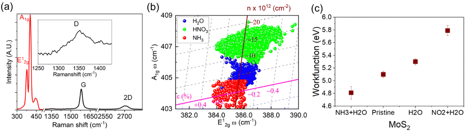 | ||
| Fig. 3 Analytes induced doping in MoS2. (a) Raman spectrum of the hybrid structure showing Raman modes of MoS2 (E12g and A1g) and few-layer graphene (G and 2D). (b) Correlation plot (E12gvs. A1g) shows the shift in peak position in the MoS2 Raman modes after exposure of solvents of dilute HNO3 (as NO2 + H2O), NH4OH (as NH3 + H2O) and H2O. (c) Trend of work function (eV) of MoS2 in different exposures of analytes. | ||
The outcomes from Raman spectroscopy are validated through surface potential measurements by KPFM (Fig. 3c), where doping characteristics of MoS2 in the heterostructured architecture are investigated separately in the exposed environment of dilute HNO3 (as a mixture of H2O and NO2) and dilute NH4OH through Kelvin probe force microscopy (KPFM). The surface potential map indicates an increase in electron concentration in the MoS2, revealing n-type doping from the substrates (see ESI† Fig. S6). In the heterostructure arrangement of MoS2 over graphite, the exposure of nitronium ions leads to p-type doping in MoS2 as compared to the subsurface graphite. In contrast, ammonium ions increase the electron concentration. The modulation in Fermi energy level in MoS2 due to adsorbates leads to alteration in the work function (∼5.1 eV) of MoS2. The adsorption of NH4+ salts decreases the work function (∼4.81 eV), while the adsorption of nitronium salt significantly increases it to ∼5.79 eV.
The charge redistribution in the graphene/MoS2 hybrid structure for different analyte molecules (H2O, NH3, and NO2) is further unravelled through density functional theory simulations. To find the best stacking configuration of MoS2 on graphene, we calculate the binding energy (Egraphene + EMoS2 − Etotal)/S for the stacking configurations shown in Fig. S7 (ESI†), where Egraphene, EMoS2, and Etotal are the total energies of graphene, MoS2, and the graphene/MoS2 hybrid structure, and S is the interfacial area (3.16 Å × 12.33 Å). With binding energies of 0.05 and 0.03 eV Å−2, the AB1 and AB configurations are energetically favourable for S- and Mo-terminated MoS2, respectively. Fig. 4a and b show that MoS2 is a charge acceptor and accepts much more charge in the case of the S-termination (0.57 electrons) than in the case of the Mo-termination (0.10 electrons). The charge redistributions between the graphene/MoS2 hybrid structure and analyte molecules are shown in Fig. 4c–e. In the proximity of the NO2 molecule close to the MoS2 edge atoms, there is a significant depletion of charge (green colour) around the sulphur atoms, due to interaction with the unpaired electron of the N atom, and an accumulation of charge on NO2 (orange colour). This charge transfer is lower for the O atom of H2O. The adsorption energy of the analyte molecule is calculated as Etotal − Egraphene/MoS2 − Emolecule, where Etotal, Egraphene/MoS2, and Emolecule are the total energies of the graphene/MoS2 hybrid structure with adsorbed molecule, the graphene/MoS2 hybrid structure without adsorbed molecule, and the analyte molecule, respectively. We find for H2O, NH3, and NO2 adsorption energies of −0.09, −0.11, and −0.13 eV, respectively. According to charge transfer analyses, the graphene/MoS2 hybrid structure with S-termination is p-doped by H2O (0.01 electrons) and NO2 (0.21 electrons), and n-doped by NH3 (0.01 electrons). The higher adsorption energy of MoS2 towards the NO2 molecule assists in more efficient charge transfer compared to the NH3 molecule. The high susceptibility to p-doping agrees with our experimental findings by Raman spectroscopy. While the graphene/MoS2 hybrid structure with Mo-termination shows similar tendencies towards the analyte molecules, see Fig. S8 (ESI†), the higher adsorption energies (−1.20 eV for H2O, −1.55 eV for NH3, and −4.42 eV for NO2) compromise the regeneration of the detector, see Table S1 (ESI†) for details.
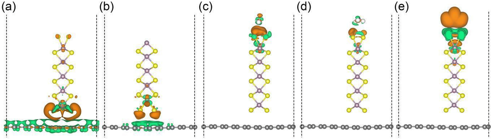 | ||
| Fig. 4 Effect of atomic arrangement on charge transfer. Side views of the charge redistributions between graphene and MoS2 with (a) S- and (b) Mo-terminations. Side views of the charge redistributions between the graphene/MoS2 hybrid structure with S-termination (towards the analyte molecules) and (c) H2O, (d) NH3, and (e) NO2. Green and orange isosurfaces (isovalue: 0.001 electrons Å−3) represent charge depletion and accumulation, respectively. The gray, yellow, purple, white, red, and blue spheres represent the C, S, Mo, H, O, and N atoms, respectively. | ||
The dynamic gas sensing response of the hybrid structure was investigated using NO2 and NH3 gases exposed to the device at controlled concentrations (Fig. 5). The investigation is conducted by cyclic exposure of the gas analyte to monitor the sensitivity, selectivity, and recovery (on each cycle) of the device. Fig. 5a and b show the typical dynamic sensing responses obtained for the hybrid structure for NO2 and NH3 analytes as the electron acceptor and donor molecules, respectively, demonstrating the selectivity of the device. During NO2 (NH3) exposure, the resistance of the hybrid-based chemiresistor decreases (increases). It reveals the different charge transport properties governed by NO2 and NH3 analytes that influence the overall conductivity of the device. After the adsorption of the oxidising gas NO2, the electron concentration in MoS2 decreases through charge transfer as shown in Fig. 4. Interaction with the unpaired electron on the N-atom shifts the Fermi level of MoS2 into its valence band (indicated by Fig. 3a and b), extracting electron charge from MoS2. In contrast, the lone pair of electrons of NH3 does not have such an effect.10 These results are in good agreement with our previous findings of p-type doping of vertically oriented MoS2 sheets over carbon nanotubes towards NO2 gas.17 Several research groups demonstrated and discussed similar p-type semiconducting behaviour of MoS2 towards NO2.10,30
 | ||
| Fig. 5 Dynamic response of hybrid structure for different concentrations of NO2 and NH3. Resistance (R/R0) profile of the chemiresistor against (a) NO2 gas and (b) NH3 gas. The arrows show the inlet and outlet of the purged gas, which influence the resistance of the chemiresistor. Resistance profile (R/R0) at 150 °C for different concentrations (ppb) of NO2 (c) and NH3 (ppm) (d). The exposure of NO2 gasses decreases resistance, while in the presence of NH3 enhances the resistance indicating p-type behavior of the hybrid structure. | ||
In the chemiresistor set-up, a slight baseline drift in the trend of the resistance profile was observed; the change in resistance during drifting is nearly 15 Ω for NO2 and ∼1 Ω for NH3 after exposure of 90 minutes (Fig. 5c and d). This drift in the resistance profile is usually experienced in carbon-based gas sensors operating at low or moderate working temperatures, which are not enough to achieve efficient and quick desorption of the analytes during the recovery phases.45 Several approaches can easily recover the original baseline in a potential real application. For instance, after a few hours of use, an increase in the temperature or the flow rate leads to better NO2/NH3 desorption, recovering the initial baseline in a few minutes. See ESI† in Fig. S9. Besides, other alternative approaches, such as the use of UV light also boost the desorption of gas molecules from the sensitive layer,46,48 which will be considered in future work. Unlike NO2 resistance profile, the trend observed in NH3 exposure shows a noisy but reproducible sub-peak (marked arrows) and slight fluctuation at the recovery phase. It indicates the susceptibility of different basal planes ([100], [002] see TEM discussion) of the MoS2 that could lead to a diverse range of surface and edge sites towards NH3 molecules that differ in the selectivity with NO2 gas analyte.
The response (ΔR/R0, %) of the individual NGF and the hybrid sensors are monitored at room temperature (RT) through purging dry air, humid conditions (relative humidity, 60%) and at elevated temperature (150 °C). The hybrid structure offers superior responses for all the testing conditions compared to its NGF counterpart. This distinction in the sensing performance is due to the abundant number of exposed edges of MoS2 nanoplates. Therefore, analyte molecules are in higher concentration at the reactive sites in the hybrid MoS2/NGF, thus enhancing the sensing response. There is an increment in the response with an increase in the NO2 analyte concentration as well as for NH3; see Fig. S10 (ESI†) for NH3. The response is further improved in humid conditions as compared to the dried atmosphere (Fig. 6a), consistent with the findings of Sakthivel and co-workers47 for enhanced sensitivity of graphene–MoS2 hybrid. As discussed in the Raman spectroscopy, KPFM investigation and density functional theory simulation, the presence of NO2 in humid conditions (i.e., H2O + NO2) induces higher p-doped MoS2 receptors by modulation of Fermi energy towards the valence band, consequently enhances the response. On close observation of the morphology of the MoS2 sheet after the exposure, it is found that the edges of the MoS2 are susceptible to salts of NO2 while NH4+ salts are distributed through the MoS2 basal plane; see Fig. S11 (ESI†). It explains the noise in the recovery phase of the chemiresistor for ammonia gas in a humid environment owing to the crucial role of the basal plane of MoS2 as an additional active site, which is limited for NO2 detection.
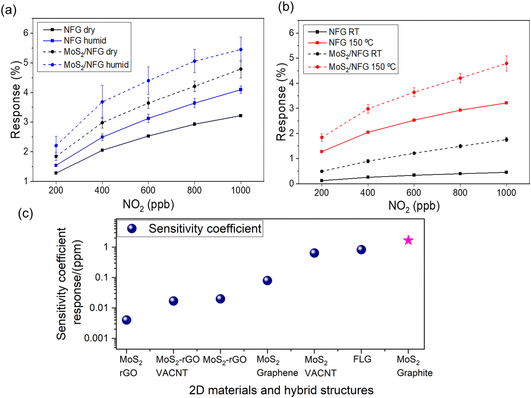 | ||
| Fig. 6 Response (%) of the hybrid sensor at different conditions. (a) Effect of humidity and dried condition in the response of the graphene layers (NGF) and hybrid sensor (MoS2/NGF). (b) Effect of temperature at 150 °C. (c) Comparison of sensing performances (Sensitivity coefficient) for NO2 detection employing 2D materials and hybrids. | ||
The sensor response is usually reduced at room temperature (RT) as compared to its thermally stimulated environment, as demonstrated in ESI† (Fig. S9 and S10). This is due to lower reactivity weaker interaction between gas molecules and the 2D materials at RT.48 The thermal activation induces better sensing kinetics, improves the recovery of the adsorbates, causes larger charge transfers for enhanced resistance changes, and influences the conduction transition.49–51 Therefore, moderately elevated temperatures in the range of 100–200 °C are generally applied to regulate the adsorption/desorption kinetics and improve the sensing performance in both carbon and dichalcogenide-based gas sensors.51 Here, we observed an overall enhancement in the response for both devices (i.e. NGF and hybrid) operated at 150 °C (Fig. 6b). Specifically, the resistance changes induced by the NO2 exposure were increased threefold and eightfold for NGF and MoS2/NGF samples, respectively. The sensitivity coefficient (rate of change of resistance normalised to applied concentration (sensing response/ppm) of 1.67 for NO2 gas for the hybrid sensor outperforms other reported 2D materials (such as few-layer graphene)52 and hybrid heterostructures (Fig. 6c). It has been observed that several MoS2-based devices and functionalised materials require operating temperatures (>200 °C) for sensing48 and thus are not suited for long-term usability and stability. A brief literature survey is reported in Table S2 (ESI†); the response of pristine MoS2 and MoS2/carbon nanomaterial hybrids towards H2, CO, CH4, and H2S has been studied, showing significantly lower responses. The present set-up operates at a moderately lower temperature (150 °C) as compared to metal oxide-based sensors attributed to the active abundant edges of MoS2 vertical morphology on conducting substrate (NGF). This is in agreement with Cho et al.30 results, by both experimental and theoretical studies demonstrating that edge sites of MoS2 can adsorb five folds higher NO2 than the basal plane MoS2 sheets in the same amount of gas exposure time.
Conclusions
The current study presents a facile method for depositing a hybrid material composed of vertically aligned MoS2 and conducting graphitic layers (NGF) on SiO2/Si. The densely-packed MoS2 flakes on NGF contribute to rationally designed edge sites for high chemiresistive sensitivity and selectivity (distinguishable p-type, n-type doping, dry-humid environment). The MoS2/NGF hybrid, tested for NO2, NH3 detection in dry, humid, and elevated temperature conditions, demonstrated superior performance compared to NGF samples. The Raman spectroscopy revealed the role of water molecules in the p-doping of MoS2, with further improvement in the presence of nitronium ions. In addition, the Raman correlation plot distinguishes changes in total carrier concentration, NO2 exposure indicates dedoping (i.e. electron transfer from MoS2 to NO2). Surface potential maps by KPFM technique validated this phenomenon by illustrating the modulation in the work function of MoS2 in NH3 and NO2 aqueous solutions. It reveals WF increase for NO2 exposure, indicating electron concentration decreased, consistent with p-doping of n-type MoS2 (and vice versa for NH3). Density functional theory calculations unravel the doping mechanism and structural importance (4 possible terminal ends) of hetero architecture towards different analytes and NGF. The hybrid sensor exhibited a sensitivity coefficient of 1.6 for NO2 at 150 °C with a LOD of 50 ppb, although NH3 measurements faced challenges due to a noisy recovery phase. Our MoS2/NGF growth studies offer a promising strategy for designing high-performance 2D material-based heterostructures in sensing technologically relevant gases in diverse environmental applications. These findings provide fundamental insights on sensing interactions resulting from the synergy between MoS2 and graphene, opening avenues for flexible electronics applications not achievable with traditional materials.Materials and methods
MoS2 synthesis
MoS2 flakes were grown by chemical vapor deposition (CVD). 100 μL of 100 mM solution of Na2MoO4 (sodium molybdate: anhydrous, powder, ∼100 mesh particle size, 99.9% trace metals basis; Sigma-Aldrich) was spin-coated at 3000 rpm for 1 minute onto solvent-cleaned Si/SiO2 (n-doped Si, 280 nm thermal oxide; University Wafer) wafer chips of 1.2 × 1.2 cm size. The spin coated substrates were placed over a ceramic boat, face-up at the center of a 2 in quartz tube in a tube furnace (Lindberg Blue Tube Furnace) and 3 g of sulfur (powder, 99.98% trace metals basis; Sigma-Aldrich) was placed in a boat 15 cm upstream. The reaction was carried out under a 100 standard cubic centimetres per minute (sccm) flow of pure Ar gas. The temperature was maintained for 20 min at 25 °C to purge the tube and then ramped up to 725 °C in 15 min. The temperature was then further ramped up to 800 °C in 5 min. After reaching the 800 °C mark, the heating was shut off and the system was allowed to cool naturally to 500 °C, after which the furnace was opened to quench-cool to ambient conditions.Graphene/MoS2 heterostructure synthesis
NGF growth and polymer support free transfer on SiO2/Si substrate was performed as discussed in detail in our recently published articles.35,36 In brief, NGF was epitaxially grown over polycrystalline Ni foils via the CVD method at growth temperature (900 °C), chamber pressure during annealing (10 bar) while keeping the flow rate constant. The polymer-free transfer of grown NGF by wet-etching, where samples were kept floating overnight in 15 ml of 70% HNO3 diluted in 600 ml of deionised (DI) water to dissolve Ni foil. The detached NGF is carefully rinsed by DI water and transferred to the target substrate (SiO2/Si wafer).MoS2 nanoplates growth
To understand the effects of the growth of MoS2 NPs on the NGF, we prepared SiO2 (300 nm)/Si samples with NGF (half covered) transferred on it (Fig. 1). In a typical procedure, Mo films of 10 and 20 nm were deposited on both uncovered SiO2/Si and NGF/SiO2/Si areas of the samples. The Mo films deposited on the NGF/SiO2/Si sample were placed in a quartz plate placed in the centre of a quartz tube. S powder was placed in two predefined zones of the tube (0.400 g were used in each zone) in order to be in the correct temperature zones when the reactor was inserted into the furnace.15,16 The S powder was used without any further purification. The quartz tube was then vacuumed and filled with Ar gas, and this process was repeated twice. Then the quartz tube was heated in a tube furnace at a rate of 5 °C min−1 in Ar (400 sccm). When the temperature reached 850 °C, the quartz tube is inserted in the hot temperature zone so as the Mo/NGF/SiO2/Si sample is at 850 °C while the S powder is at 250 °C. The deposition time was kept 30 min similar to previous cases of MoS2 growth.15,16 After the reaction time, the tube was cooled to room temperature in Ar gas.Characterisation techniques
Scanning electron microscopy (SEM) was performed by a Zeiss Merlin (5 kV, 50 pA) microscope. The sample surface roughness and topography was recorded via atomic force microscopy (AFM, Dimension Icon SPM, Bruker). The transmission electron microscopy (TEM) and high-resolution TEM (HRTEM) investigations were performed with a ThemoFisher Titan 80–300 Cubed microscope equipped with a high-brilliance field emission gun operating at 300 kV, a Wien-type FEI monochromator, and an objective lens CEOS spherical aberration corrector allowing a final spatial resolution of 0.9 Å. For both TEM and HR-TEM imaging analysis, we used a direct detection Ametek Gatan K2 IS camera. Plan-view TEM samples were prepared by scratching the specimen's surface and collecting the powder material directly onto lacey-carbon coated Cu grids. The cross-section lamella was prepared with a FEI Helios G4 focused ion beam (FIB) SEM microscope, equipped with a field emission gun and a Leica cryo-holder stage. To protect the MoS2 NPs region of interest, we coated the sample with a 5 nm layer of Ir and 1.5 μm of Pt. Then, the milling procedure was carried out, with the cryo-stage set at −145 °C and by the use of an ion beam of 16 kV (to reduce sample damage and artifacts formation) with a current range of 10 nA to 12 pA. Once completed, the thin lamella was slowly warmed up to room temperature.Kelvin Probe force microscopy
Kelvin Probe Force Microscopy (KPFM) is carried out at room temperature by Bruker AFM (model: ScanAsyst) using a cantilever (model: PFQNE-AL). A single layer of the CVD MoS2 has been used for the investigation, where it is treated with different analytes and surface potential has been measured. The KPFM measurement is carried through the two-pass technique, where the first pass is used to scan the topography of the sample, and the second pass is carried out at a specific lift height to measure the contact potential difference (CPD, mV). The reference sample (Au–Si–Al) has been used to calibrate the cantilever probe apex and measure the sample's work function (eV).Raman spectroscopy
Raman spectroscopy (model: Renishaw) has been carried out using laser line (λ = 532 nm, grating 1800 l/mm and magnification 100×) over the samples. The spectra and mapping were carried out at a similar location for the pre and post-treated samples. More than 500 Raman spectra were carried out using different samples. All Raman shifting values were measured through Lorentzian fitting of the Raman modes and compared to its native state. Si sample was used for the calibration of the Raman spectrometer. A separate measurement is carried out using spectrometer (Alpha 300 RA, WITeC, 532 nm laser, 100×, lateral resolution 0.5) to verify the peak position and Raman shifts.It is worth noting that the surface potential mapping and Raman spectroscopy is carried out in the presence of ammonium and nitronium ions, where salts are considered in the presence of water molecules. Our KPFM and Raman spectroscopy set-up is limited to study for gaseous analytes.
X-ray diffraction
The X-ray diffraction (XRD) analysis has been performed on NGF/SiO2/Si before and after MoS2 NPs growth with a powder a Brucker diffractometer equipped with D2 phaser and LYNXEYE detector and operating with a Cu radiation source.X-ray photoelectron spectroscopy (XPS)
The chemical properties of the sample have been investigated by X-ray photoelectron spectroscopy, performed on Thermo K-Alpha spectrometer using Al Kα source (1486.68 eV) and a spot size of 250 × 250 μm2. Before analysis, the sample surface has been cleaned with a cluster beam (Ar500+, 2 keV, 120 s, raster size of 1.25 × 1.25 mm2). The high-resolution spectra of C 1s, O 1s, S 2p, and Mo 3d levels are recorded at pass energy of 20 eV, with 20 scans. The atomic concentrations were determined from the area of each peak, considering a Shirley background.Gas-sensing device fabrication and measurements
The MoS2/NGF/SiO2/Si samples were connected to 20 × 30 mm printed circuit boards (PCBs) through two platinum wire contacts made on the sensor surface using conductive silver paste from Merck KGaA (Darmstadt, Germany). This silver paste is often used to electrically contact devices to be operated in harsh conditions such as ultra-high vacuum or under heating (e.g. in synchrotron experiments), as it does not degases. Sample resistance was measured in a two-contact (two-probe) configuration. Namely, the multimeter applies a constant voltage between the two contacts and measures the current. In such a simple configuration, the resistance measured comprises the sample resistance and the contact resistance. The platinum screen-printed alumina heating element was connected at the backside of the sample using a thermally conducting epoxy paste.Both sensors NGF and MoS2/NGF/SiO2/Si were placed in an airtight Teflon testing chamber, with a volume of 35 cm3. This chamber was connected to a gas delivery system, which comprised two calibrated gas cylinders, one with pure dry air (Air Premier Purity: 99,995%) and the other with 1 ppm of NO2 in a balance of dry air. Different dilutions of the target gases were performed to expose the sensors at different concentrations of NO2, NH3 in the range of parts per billion (ppb). Specifically, the gas sensors were stabilised under synthetic dry air for 15 minutes before every gas exposure and then exposed to a given concentration of NO2 for 5 minutes. Besides, the effect of the ambient moisture on the sensing properties was also assessed. A controller evaporator mixer (CEM) from Bronkhorst High-Tech B.V. (Ruurlo, The Netherlands) was used to humidify the gas mixture, and the relative humidity level was monitored by using a humidity sensor from Sensirion AG (Stäfa, Switzerland) placed inside the Teflon chamber. When the sensors were operated well above room temperature, they were connected to a Keysight E3641A (Santa Rosa, CA, U.S.) power supply.
In order to operate the system under similar conditions to those needed for ambient monitoring applications, a low flow rate was applied, avoiding the use of pumps. In particular, a set of Bronkhorst High-Tech B.V. (Ruurlo, The Netherlands) mass-flows controllers were used to establish a flow rate of 100 mL min−1. Finally, the changes in sensor resistance were monitored using an Agilent HP 34972A multimeter connected to the sensing chamber. The sensor responses were defined as (ΔR/R0) expressed in percentage. Where ΔR is the resistance change over the five minutes of gas exposure, while R0 corresponds to the baseline resistance obtained under the pure air atmosphere.
Thereby, the slope of our sensor at 150 °C for measuring NO2 at the ppb level results in a 0.00167 response per ppb (.(0.00167 response/ppb) × (1000 ppb/1 ppm) = 1.67 response/ppm)
Computational method
First-principles calculations are performed using density functional theory (Vienna Ab-initio Simulation Package) and the generalised gradient approximation of Perdew–Burke–Ernzerhof with DFT-D3 van der Waals correction.53 The plane wave cutoff energy is set to 500 eV. The total energy is converged to 10−5 eV and the atomic forces are converged to 0.01 eV Å−1. A Monkhorst–Pack k-sampling with 0.015 Å−1 spacing is used. To achieve a small lattice mismatch (2% in the b-direction), we build our simulation cells from the supercells of graphene and MoS2 shown in Fig. S7a and b (ESI†). Vacuum slabs of at least 15 Å thickness (in the c-direction) avoid unphysical interaction due to the periodic boundary conditions. Charge transfer analyses are performed by the Bader method.54Conflicts of interest
There are no conflicts to declare.Acknowledgements
MT and ABD would like to thank the University of Sussex strategic development fund. This work was supported by KAUST (BAS/1/1346-01-01). For computer time, this research used the resources of the Supercomputing Laboratory at KAUST. The SIAM platform from the University of Namur is acknowledged for XPS measurement. E. L. is supported by the Catalan Institution for Research and Advanced Studies via the 2023 Edition of the ICREA Academia Award. This work was also partially supported by a UKRI Future Leaders Fellowship [grant number MR/T042664/1]. VG acknowledge the funding support from National Science Foundation RII FEC awards (#1849206, #1920954).References
- I. Manisalidis, E. Stavropoulou, A. Stavropoulos and E. Bezirtzoglou, Front. Public Health, 2020, 8, 14 CrossRef PubMed.
- D. J. Buckley, N. C. Black, E. G. Castanon, C. Melios, M. Hardman and O. Kazakova, 2D Mater., 2020, 7, 032002 CrossRef CAS.
- S. M. Majhi, A. Mirzaei, H. W. Kim, S. S. Kim and T. W. Kim, Nano Energy, 2021, 79, 105369 CrossRef CAS PubMed.
- A. Dey, Mater. Sci. Eng. B, 2018, 229, 206–217 CrossRef CAS.
- H. Chai, Z. Zheng, K. Liu, J. Xu, K. Wu, Y. Luo, H. Liao, M. Debliquy and C. Zhang, IEEE Sens. J., 2022, 22, 5470–5481 CAS.
- B. Cho, J. Yoon, S. K. Lim, A. R. Kim, D.-H. Kim, S.-G. Park, J.-D. Kwon, Y.-J. Lee, K.-H. Lee and B. H. Lee, ACS Appl. Mater. Interfaces, 2015, 7, 16775–16780 CrossRef CAS PubMed.
- U. Krishnan, M. Kaur, K. Singh, M. Kumar and A. Kumar, Superlattices Microstruct., 2019, 128, 274–297 CrossRef CAS.
- T. Zeng, Y. You, X. Wang, T. Hu and G. Tai, Prog. Chem., 2016, 28, 459 CAS.
- K. F. Mak, C. Lee, J. Hone, J. Shan and T. F. Heinz, Phys. Rev. Lett., 2010, 105, 136805 CrossRef PubMed.
- R. Kumar, W. Zheng, X. Liu, J. Zhang and M. Kumar, Adv. Mater. Technol., 2020, 5, 1901062 CrossRef CAS.
- F. Schedin, A. K. Geim, S. V. Morozov, E. W. Hill, P. Blake, M. I. Katsnelson and K. S. Novoselov, Nat. Mater., 2007, 6, 652–655 CrossRef CAS PubMed.
- G. Deokar, N. S. Rajput, J. Li, F. L. Deepak, W. Ou-Yang, N. Reckinger, C. Bittencourt, J.-F. Colomer and M. Jouiad, Beilstein J. Nanotechnol., 2018, 9, 1686–1694 CrossRef CAS PubMed.
- Y. Huang, J. Guo, Y. Kang, Y. Ai and C. M. Li, Nanoscale, 2015, 7, 19358–19376 RSC.
- A. Allain and A. Kis, ACS Nano, 2014, 8, 7180–7185 CrossRef CAS PubMed.
- G. Deokar, N. S. Rajput, P. Vancsó, F. Ravaux, M. Jouiad, D. Vignaud, F. Cecchet and J. F. Colomer, Nanoscale, 2017, 9, 277–287 RSC.
- G. Deokar, D. Vignaud, R. Arenal, P. Louette and J.-F. Colomer, Nanotechnology, 2016, 27, 075604 CrossRef CAS PubMed.
- G. Deokar, P. Vancso, R. Arenal, F. Ravaux, J. Casanova-Cháfer, E. Llobet, A. Makarova, D. Vyalikh, C. Struzzi and P. Lambin, Adv. Mater. Interfaces, 2017, 4, 1700801 CrossRef.
- Q. H. Wang, K. Kalantar-Zadeh, A. Kis, J. N. Coleman and M. S. Strano, Nat. Nanotechnol., 2012, 7, 699–712 CrossRef CAS PubMed.
- Y. H. Lee, X. Q. Zhang, W. Zhang, M. T. Chang, C. T. Lin, K. D. Chang, Y. C. Yu, J. T. W. Wang, C. S. Chang and L. J. Li, Adv. Mater., 2012, 24, 2320–2325 CrossRef CAS PubMed.
- Y.-S. Shim, K. C. Kwon, J. M. Suh, K. S. Choi, Y. G. Song, W. Sohn, S. Choi, K. Hong, J.-M. Jeon and S.-P. Hong, ACS Appl. Mater. Interfaces, 2018, 10, 31594–31602 CrossRef CAS PubMed.
- F. Xiong, Z. Cai, L. Qu, P. Zhang, Z. Yuan, O. K. Asare, W. Xu, C. Lin and L. Mai, ACS Appl. Mater. Interfaces, 2015, 7, 12625–12630 CrossRef CAS PubMed.
- W. Li, Y. You and J.-H. Choi, Surf. Sci., 2021, 707, 121809 CrossRef CAS.
- E. Lee, S. G. Lee, W. H. Lee, H. C. Lee, N. N. Nguyen, M. S. Yoo and K. Cho, Chem. Mater., 2020, 32, 4544–4552 CrossRef CAS.
- Y. Chen and M. Sun, Nanoscale, 2021, 13, 5594–5619 RSC.
- Y. Yuan, X. Zhang, H. Liu, T. Yang, W. Zheng, B. Zheng, F. Jiang, L. Li, D. Li and X. Zhu, J. Alloys Compd., 2020, 815, 152309 CrossRef CAS.
- X. Yu, G. Zhao, S. Gong, C. Liu, C. Wu, P. Lyu, G. Maurin and N. Zhang, ACS Appl. Mater. Interfaces, 2020, 12, 24777–24785 CrossRef CAS PubMed.
- L. Yu, Y.-H. Lee, X. Ling, E. J. Santos, Y. C. Shin, Y. Lin, M. Dubey, E. Kaxiras, J. Kong and H. Wang, Nano Lett., 2014, 14, 3055–3063 CrossRef CAS PubMed.
- B. Sachs, L. Britnell, T. Wehling, A. Eckmann, R. Jalil, B. Belle, A. Lichtenstein, M. Katsnelson and K. Novoselov, Appl. Phys. Lett., 2013, 103, 251607 CrossRef.
- W. Zan, W. Geng, H. Liu and X. Yao, J. Alloys Compd., 2015, 649, 961–967 CrossRef CAS.
- S.-Y. Cho, S. J. Kim, Y. Lee, J.-S. Kim, W.-B. Jung, H.-W. Yoo, J. Kim and H.-T. Jung, ACS Nano, 2015, 9, 9314–9321 CrossRef PubMed.
- G. Ciampalini, F. Fabbri, G. Menichetti, L. Buoni, S. Pace, V. Mišeikis, A. Pitanti, D. Pisignano, C. Coletti and A. Tredicucci, ACS Nano, 2021, 16, 1291–1300 CrossRef PubMed.
- Y. Shi, W. Zhou, A.-Y. Lu, W. Fang, Y.-H. Lee, A. L. Hsu, S. M. Kim, K. K. Kim, H. Y. Yang and L.-J. Li, Nano Lett., 2012, 12, 2784–2791 CrossRef CAS PubMed.
- M. Chatti, T. Gengenbach, R. King, L. Spiccia and A. N. Simonov, Chem. Mater., 2017, 29, 3092–3099 CrossRef CAS.
- Z. Mao, H. Zhu, X. Peng, J. Chen, Q. Chen, X. Chen, X. Hu and H. Chen, Microchim. Acta, 2022, 189, 155 CrossRef CAS PubMed.
- G. Deokar, A. Genovese and P. M. Costa, Nanotechnology, 2020, 31, 485605 CrossRef CAS PubMed.
- G. Deokar, A. Genovese, S. G. Surya, C. Long, K. N. Salama and P. M. F. J. Costa, Sci. Rep., 2020, 10, 14703 CrossRef CAS PubMed.
- M.-C. Chang, P.-H. Ho, M.-F. Tseng, F.-Y. Lin, C.-H. Hou, I. K. Lin, H. Wang, P.-P. Huang, C.-H. Chiang and Y.-C. Yang, Nat. Commun., 2020, 11, 3682 CrossRef CAS PubMed.
- J. Kong, K. T. Park, A. Miller and K. Klier, Surf. Sci. Spectra, 2000, 7, 69–74 CrossRef CAS.
- D. Ganta, S. Sinha and R. T. Haasch, Surf. Sci. Spectra, 2014, 21, 19–27 CrossRef CAS PubMed.
- X. Ai, H. Fan, Y. Wang, Y. Guo, X. Liu, L. Yang, H. Liu and J. Yang, RSC Adv., 2018, 8, 36280–36285 RSC.
- T.-X. Huang, X. Cong, S.-S. Wu, K.-Q. Lin, X. Yao, Y.-H. He, J.-B. Wu, Y.-F. Bao, S.-C. Huang and X. Wang, Nat. Commun., 2019, 10, 5544 CrossRef CAS PubMed.
- F. Lee, M. Tripathi, R. Sanchez Salas, S. P. Ogilvie, A. Amorim Graf, I. Jurewicz and A. B. Dalton, Nanoscale, 2023, 15, 7227–7248 RSC.
- M. Tripathi, F. Lee, A. Michail, D. Anestopoulos, J. G. McHugh, S. P. Ogilvie, M. J. Large, A. A. Graf, P. J. Lynch and J. Parthenios, ACS Nano, 2021, 15, 2520–2531 CrossRef CAS PubMed.
- J. H. Kim, J. Lee, J. H. Kim, C. Hwang, C. Lee and J. Y. Park, Appl. Phys. Lett., 2015, 106, 251606 CrossRef.
- H. Du, G. Xie, Y. Su, H. Tai, X. Du, H. Yu and Q. Zhang, Sensors, 2019, 19, 889 CrossRef PubMed.
- A. Di Bartolomeo, A. Kumar, O. Durante, A. Sessa, E. Faella, L. Viscardi, K. Intonti, F. Giubileo, N. Martucciello, P. Romano, S. Sleziona and M. Schleberger, Mater. Today Nano, 2023, 24, 100382 CrossRef CAS.
- R. Sakthivel, A. Geetha, B. Anandh, V. Jagadeesan, A. S. Ganesh and J. Dineshkumar, J. Phys.: Conf. Ser., 2021, 2070, 012131 CrossRef.
- P. Srinivasan, M. Ezhilan, A. J. Kulandaisamy, K. J. Babu and J. B. B. Rayappan, J. Mater. Sci.: Mater. Electron., 2019, 30, 15825–15847 CrossRef CAS.
- D. Mouloua, A. Kotbi, G. Deokar, K. Kaja, M. El Marssi, M. A. El Khakani and M. Jouiad, Materials, 2021, 14, 3283 CrossRef CAS.
- R. Kumar, X. Liu, J. Zhang and M. Kumar, Nano-Micro Lett., 2020, 12, 1–37 CrossRef PubMed.
- H. Xie, K. Wang, Z. Zhang, X. Zhao, F. Liu and H. Mu, RSC Adv., 2015, 5, 28030–28037 RSC.
- G. Deokar, J. Casanova-Chafer, N. S. Rajput, C. Aubry, E. Llobet, M. Jouiad and P. M. Costa, Sens. Actuators, B, 2020, 305, 127458 CrossRef CAS.
- G. Kresse and D. Joubert, Phys. Rev. B: Condens. Matter Mater. Phys., 1999, 59, 1758 CrossRef CAS.
- W. Tang, E. Sanville and G. Henkelman, J. Phys.: Condens. Matter, 2009, 21, 084204 CrossRef CAS PubMed.
Footnotes |
| † Electronic supplementary information (ESI) available. See DOI: https://doi.org/10.1039/d4nh00049h |
| ‡ Authors contributed equally. |
| This journal is © The Royal Society of Chemistry 2024 |