
A synergistic heterojunction of SnS2/SnSSe nanosheets on GaN for advanced self-powered photodetectors†
Sukhendu
Maity
 and
Praveen
Kumar
*
and
Praveen
Kumar
*
School of Materials Science, Indian Association for the Cultivation of Science, Kolkata 700032, India. E-mail: praveen.kumar@iacs.res.in
First published on 9th May 2024
Abstract
Tin-based TMDCs are gaining traction in optoelectronics due to their eco-friendliness and easy synthesis, contrasting Mo/W-based counterparts. This study pioneers the solvothermal synthesis of highly crystalline SnSSe alloy, akin to Janus structures, bridging a notable research gap. By integrating SnS2/SnSSe materials onto a GaN platform, a synergistic heterojunction is created, enhancing light absorption and the electron–hole pair separation efficiency, demonstrating a self-powered photodetection. The GaN/SnS2/SnSSe heterojunction showcases a staircase-like (type-II) band alignment and exceptional performance metrics: high photoresponsivity of 314.96 A W−1, specific detectivity of 2.0 × 10¹⁴ jones, and external quantum efficiency of 10.7 × 10⁴% under 365 nm illumination at 150 nW cm−2 intensity and 3 V bias. Notably, the device displays intensity-dependent photocurrent and photoswitching behaviors without external bias, highlighting its unique self-powered attributes. This study underscores SnS2's significance in optoelectronics and explores SnSSe integration into van der Waals heterostructures, promising advanced photodetection devices and bias-free optoelectronics.
New conceptsThis study breaks new ground in optoelectronics by exploring the untapped potential of tin-based transition metal dichalcogenides (TMDCs). Utilizing innovative solvothermal synthesis techniques, highly crystalline SnS2 and SnSSe alloys, resembling Janus structures, are synthesized. The integration of these materials into van der Waals heterostructures on a GaN platform introduces novel concepts in device engineering, enhancing light absorption and the electron–hole pair separation efficiency. Particularly noteworthy is the introduction of SnSSe-based self-powered photodetection, demonstrating unprecedented performance metrics and unique intensity-dependent behaviors. These innovations pave the way for advanced photodetection devices, heralding a paradigm shift towards bias-free optoelectronics in materials science. |
1. Introduction
In recent decades, symmetric 2D transition metal dichalcogenides (TMDCs) have captured significant attention in the scientific community owing to their remarkable properties, such as a large surface-to-volume ratio, high surface activities, and tunable bandgaps, rendering them pivotal components for next-generation optoelectronic devices.1–6 TMDCs, with the general formula MX2 (where M represents transition metals like Mo, W, Sn, Nb, Zr, and X denotes chalcogens such as S, Se, and Te), can be easily exfoliated into monolayers or few-layers, enabling bandgap tuning and utilization in various photosensitive devices.7–10 While MoS2 and WS2 have been extensively studied and are more accessible, their limited abundance on Earth and complex synthesis processes raise costs, hindering their industrial-scale application in optoelectronics. To address these challenges, Tin dichalcogenide (SnS2) emerges as a promising alternative due to its abundant and eco-friendly nature, coupled with excellent absorption coefficients in the UV-visible region and rapid diffusion rates of electron–hole pairs, showing immense potential in diverse photosensitive devices.11,12 SnS2, an exceptional n-type semiconducting 2D material with an indirect bandgap of 2.18–2.42 eV, possesses a layered CdI2 type structure, where Sn atoms are sandwiched between layers of hexagonally close-packed S atoms, bonded by weak van der Waals interactions.13–16 Recently, Sn(SxSe1−x)2, a 2D ternary semiconductor alloy, has garnered significant interest due to its composition-dependent bandgap tunability and other remarkable properties.17,18 Earlier investigations suggest that the interlayer spacing of SnSSe expands by 2.84% compared to SnS2, aiding in the efficient stripping of lamellar materials.19 This structural variation is particularly advantageous for applications requiring enhanced accessibility to the material's layers. Moreover, groundbreaking studies have shown that doping a part of the sulfur element in selenide could increase the concentration of electron and hole carriers, thereby improving the conductivity.20 Simultaneously, the sulphuration on selenides can enhance the donor states of the surface sulfur, contributing to the overall enhancement of the material's electronic properties.21 Although SnS2 and SnSSe have been synthesized successfully using various methods, their individual utilization encounters obstacles in achieving high detectivity owing to minimal light absorption and inadequate band alignment for effective charge transport, especially when lacking suitable substrates.22–25 To leverage the benefits of both 2D layered materials and matured 3D process technologies, researchers have integrated layered 2D TMDCs with conventional 3D semiconductor substrates, leading to the development of novel optoelectronic devices.26 Vertical heterostructures between Si and SnS2 have shown promise in achieving high light absorption, efficient charge separation and a rectification ratio of ∼104; however, issues such as large dark currents have limited their detectivity.27 Therefore, researchers are actively exploring van der Waals heterostructures, formed by stacking 2D materials with weak interlayer interactions, to capitalize on unique properties advantageous for photodetector applications.28,29 Leveraging this technique, Li et al. reported extraordinary responsivity exceeding 2600 A W−1 in h-BN/p-MoTe2/graphene/n-SnS2/h-BN van der Waals (vdW) heterostructures fabricated through layer-by-layer dry transfer.30 Furthermore, self-powered photodetectors (PDs), capable of autonomous, wireless, and sustainable operation, have garnered considerable attention to fulfil the requirements of lightweight, compact size, and low power consumption for future optoelectronic devices. Typically, the intrinsic electric field is induced by forming p–n heterojunctions, enhancing the separation efficiency of photoexcited electron–hole pairs and consequently improving the photoelectric properties. Moreover, the photovoltaic effect of p–n heterojunctions can facilitate high self-powered phenomena, offering greater opportunities and potential for the advancement of self-powered photodetectors (PDs). Kumar et al. introduced the integration of distinctive 3D architecture nanoflowers (NFs) derived from 2D metal chalcogenide (MC) nanoflakes (SnS2 and SnSe2) onto a silicon (Si) substrate via the hydrothermal method, establishing heterojunctions to advance self-powered photodetector (PD) devices.31 The resulting Si/SnS2 heterostructures demonstrate a responsivity of 0.0125 mA W−1 and a detectivity of 2.85 × 10⁷ jones under 365 nm illumination in self-powered mode. Chen et al. have also conducted similar research, presenting a vertical SnS2/GaN p–n heterojunction (type-II) fabricated through a combination of physical vapor deposition (PVD) and chemical vapor deposition (CVD) techniques for self-powered deep-ultraviolet photodetectors.11 Jiang et al. presented thin film vertical heterojunction photodetectors (PDs) composed of ITO/SnS2/ZnO1−xSx/Ti/Au, fabricated via magnetron sputtering for self-powered photodetector applications.12 The excellent device performance is attributed to the type II band alignment of the SnS2/ZnO1−xSx heterojunction, along with the Schottky barrier formed at the ITO/SnS2 interface. The self-powered device exhibits outstanding responsivity of 8.28 mA W−1 and a detectivity of 5.09 × 10¹⁰ jones at 365 nm. Now, interlayer recombination in p–n van der Waals (vdW) heterostructures is chiefly governed by the disparity in carrier concentration between the two material components. Notably, if this difference is significant, Shockley–Read–Hall (SRH) recombination stemming from interfacial defects/traps will prevail. Consequently, addressing the mitigation of defects/trap states at the nanoscale interface is pivotal for advancing the device performance of such 2D vdW heterostructures.32 Yan et al. addressed this challenge by developing a highly sensitive unipolar barrier photodetector (InSe/SnS2/GeSe heterostructure). The distinct barrier effectively prevents dark tunnelling current while permitting the photocurrent, resulting in high responsivity and detectivity. The InSe/SnS2/GeSe photodetector demonstrated a peak responsivity of 1.87 A W−1 and a peak detectivity (D) of 8.39 × 10¹² jones under 355 nm laser illumination.33 Heterojunction interfaces often harbor defect states stemming from lattice mismatch and significant variations in work function, leading to heightened dark current even under zero bias conditions. To mitigate this issue, Abbas et al. presented a photodetector employing a SnO2/SnS2 heterojunction with an In2O3 interlayer for self-powered operation. Through this approach, they achieved a reduction in dark current (from 6.9 to 2.8 μA) alongside a simultaneous increase in photocurrent (from 11.6 to 14.7 μA). The fabricated devices exhibited a responsivity of 2.9 mA W−1 and a detectivity of 5.9 × 10⁷ jones.34This study introduces an innovative photodetector featuring a GaN/SnS2/SnSSe van der Waals heterojunction, demonstrating a self-powered UV photoresponse. A key novelty lies in the first-ever solvothermal synthesis of highly crystalline SnS2 and Sn(SxSe1−x)2 alloy (where x ≈ 0.6), closely resembling Janus structures. Comprehensive characterization via X-ray diffraction, electron microscopy, Raman spectroscopy, and X-ray photoelectron spectroscopy validates their crystallinity and purity, comparable to materials grown through chemical vapor deposition (CVD). Moreover, the validation of charge transfer between SnS2 and SnSSe through photoluminescence (PL) quenching and time-correlated single photon counting (TCSPC) measurements adds to the novelty. The successful achievement of van der Waals heterostructures of these transition metal dichalcogenides (TMDCs) on a GaN substrate using a straightforward spray coat technique is significant. Fabrication of three type II vertical heterojunction-based photodetector devices: (a) GaN/SnSSe; (D1), (b) GaN/SnS2; (D2), and (c) GaN/SnS2/SnSSe; (D3), reveals dynamic behavior, with both intensity and bias-dependent photoswitching under 365 nm illuminations. Notably, substantial enhancements in photodetection parameters, including responsivity and detectivity, are observed, alongside a reduction in response time for the GaN/SnS2/SnSSe-based device. The optimized heterostructure demonstrates remarkable photoresponsivity of 314.96 A W−1, specific detectivity of 2.0 × 10¹⁴ jones, and external quantum efficiency of 10.7 × 10⁴% under 365 nm illumination at an intensity of 150 nW cm−2 and at a bias of 3 V. Noteworthy is the observation of well-defined intensity-dependent photocurrent and photo switching in the absence of external bias in the fabricated type-II double heterojunction-based devices. Additionally, density functional theory (DFT) studies, focusing on electron density distribution (EDD), elucidate improved charge separation and transport mechanisms within the GaN/SnS2/SnSSe-based hybrid 2D/3D heterostructure.
2. Experimental
2.1 Materials and chemical
Commercially available undoped GaN grown on c-sapphire (Al2O3) (0001) was used as a substrate. For synthesizing bulk SnS2, and Sn(SxSe1−x)2, sodium stannate trihydrate ((Na2SnO3·3H2O), ≥98%, Sigma Aldrich) as a source for Sn, thiourea ((CH4N2S), ≥99.9%, Merck) as a source for S, elemental selenium powder ((Se), 99.99%, Merck) and hydrazine hydrate ((N2H4), 80%, Merck), dimethylformamide ((C3H7NO), ≥99.9%, Merck), and deionized water ((H2O), Merck) were used as precursors.2.2 Solvothermal synthesis of bulk SnS2 and Sn(SxSe1−x)2
Bulk SnS2 was synthesized using a conventional solvothermal method. Initially, 533.5 mg of Na2SnO3·3H2O was dissolved in 10 mL of deionized water through 15 minutes of sonication. In another beaker, 609 mg of thiourea was mixed with 32 mL of DMF and 8 mL of hydrazine hydrate and stirred at 1000 rpm for 30 minutes. The sulfur source was slowly added to the Sn salts drop-wise, and the mixture was stirred at 1000 rpm for 30 minutes. The resulting solution was transferred to a 100 mL Teflon-lined stainless-steel autoclave and heated at 180 °C for 18 hours. After cooling, the precipitate was collected through centrifugation, washed with DI water several times, and vacuum-dried overnight. The SnS2 raw sample underwent further annealing at 400 °C under an argon gas atmosphere for 3 hours. For Sn(SxSe1−x)2 synthesis, similar procedures were followed with 304.5 mg of thiourea and 316 mg of elemental selenium powder placed in two separate beakers with 20 mL of DMF and 6 mL of hydrazine hydrate, respectively.2.3 Device fabrication
Following the synthesis of crystalline bulk SnS2 and Sn(SxSe1−x)2, they underwent exfoliation in isopropanol at a concentration of 1 mg mL−1 using a probe sonicator operating at a frequency of 20 kHz (LAB MAN, PRO650, India) for 4 hours. The GaN substrate was subjected to a cleaning process involving successive sonication in acetone, isopropyl alcohol, and deionized water, with each step lasting 10 minutes. Additionally, the substrate underwent HF deep rinsing to eliminate residual dust. Subsequently, the exfoliated transition metal dichalcogenides (TMDCs), including SnS2 and SnSSe, were deposited onto the cleaned GaN substrate using a simple spray coating method at a temperature of 115 °C. After the spray coating, the substrates were placed at 150 °C under vacuum to eliminate any residual solvent from the surface. Copper wires were connected to both sides of the junction using conducting silver paste (Ted Pella). The various steps involved in this process are schematically presented in Fig. 1.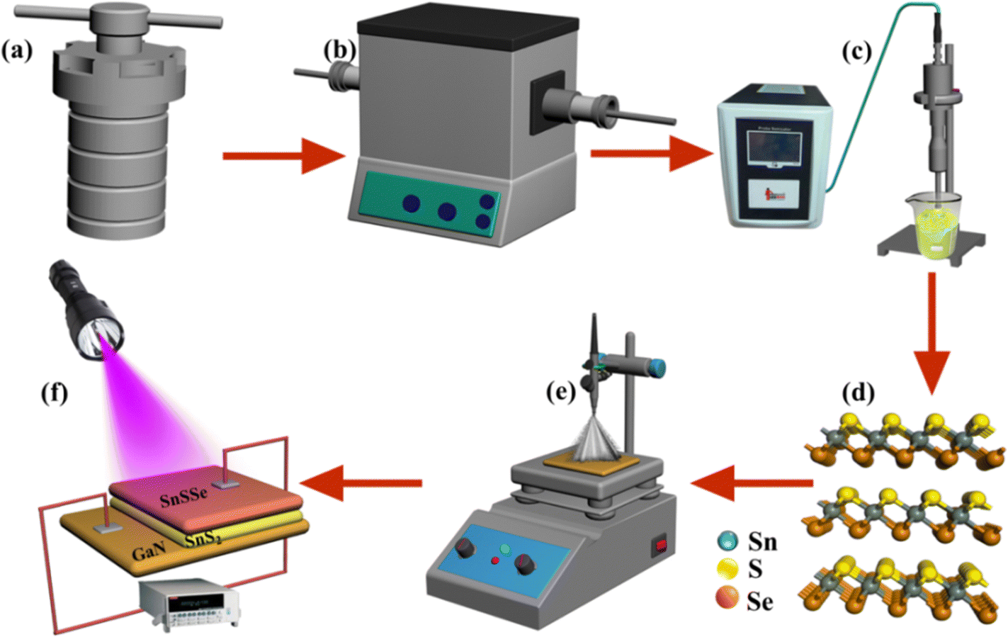 | ||
| Fig. 1 Schematic of (a) solvothermal synthesis of TMDCs, (b) annealing of TMDCs under an inert atmosphere for better crystallinity, (c) mechanical exfoliation by probe sonication, (d) 2D TMDCs, (e) device fabrication by the spray coating technique, and (f) the final device under UV radiation. | ||
2.4 Characterization
The crystal structure of bulk SnS2, Sn(SxSe1−x)2, powder, and the final thin film devices (GaN/SnS2, GaN/Sn(SxSe1−x)2, GaN/SnS2/Sn(SxSe1−x)2) were investigated using X-ray diffraction conducted with a Pan analytical X-ray diffractometer (SmartLab, HyPix-3000). Raman Spectroscopy analysis was performed using a Horiba Scientific instrument with model no: T64000 equipped with a 532 nm DPSS laser. To assess the optical properties of both SnS2 and Sn(SxSe1−x)2, UV-Vis absorption spectroscopy was conducted using a Varian Cary 5000 UV-Vis-NIR spectrophotometer. Crystal structure and layer information were obtained using field emission gun transmission electron microscopy (FEG-TEM, JEOL, JEM 2100F). The surface morphologies were examined through atomic force microscopy (AFM, VEECO CPII) and field emission scanning electron microscopy (FESEM, JEOL JSM 7500F), respectively. The composition and chemical purity of the prepared SnS2 and Sn(SxSe1−x)2 were analyzed using X-ray photoelectron Spectroscopy with a PHI 500 Versa Probe II System equipped with a monochromatic Al Kα source. Carrier lifetime was measured using time-correlated single-photon counting (TCSPC) with DeltaFlex, Horiba Scientific. Current–voltage (I–V) measurements of the fabricated devices were conducted using a Keithley 6487 source measure unit under voltage sweeping and DC mode under 365 nm light (UV A lamps, Osram-made). The intensity of the incoming light to the device was adjusted using a standard UV-A intensity meter (Lutron UV-340A UV light meter).2.5 Density functional theory simulations
To theoretically investigate the enhancement of the photocurrent and fast switching characteristics observed in the GaN/SnS2/SnSSe heterojunction, we employed the CASTEP (Cambridge Sequential Total Energy Package) program, based on density functional theory (DFT) with the projector augmented wave (PAW) approach for ion–electron interaction.35 In our calculations, we utilized the generalized gradient approximation (GGA) in the form of the Perdew–Burke–Ernzerhof (PBE) function for exchange–correlation effects. Additionally, the DFT-D method was applied to account for van der Waals interactions. Structural relaxation was performed using the Broyden–Fletcher–Goldfarb–Shanno (BFGS) algorithm scheme, with a plane wave basis cut-off energy of 720 eV and a Monkhorst–Pack 5 × 5 × 1 k-point mesh. For geometry optimization, convergence tolerance, shifting, force, and tension were set to 1 × 10⁻⁶ eV per atom, 5.0 × 10⁻⁴ Å, 0.01 eV per atom, and 0.02 GPa, respectively. The lattice constants of SnS2 and SnSSe were determined as (a = b = 3.65 Å, c = 5.917 Å) and (a = b = 3.706 Å, c = 6.024 Å) with space groups P![[3 with combining macron]](https://www.rsc.org/images/entities/char_0033_0304.gif) m1; (164) and P3m1; (156), respectively, derived from the XRD pattern of SnS2 and SnSSe. To prevent interaction between the periodic structures (SnS2/SnSSe), a slab model containing both SnS2 and SnSSe with a vacuum space of 20 Å was employed. The electronic properties of the SnS2/SnSSe heterostructures were evaluated using the Brillouin zone path Γ → A → H → K → Γ → M → L → H with the GGA-PBE method.
m1; (164) and P3m1; (156), respectively, derived from the XRD pattern of SnS2 and SnSSe. To prevent interaction between the periodic structures (SnS2/SnSSe), a slab model containing both SnS2 and SnSSe with a vacuum space of 20 Å was employed. The electronic properties of the SnS2/SnSSe heterostructures were evaluated using the Brillouin zone path Γ → A → H → K → Γ → M → L → H with the GGA-PBE method.
3. Results and discussion
The structural properties of the synthesized bulk SnS2 and Sn(SxSe1−x)2 powder and thin films were meticulously investigated using XRD and Raman spectroscopy. In Fig. 2(a) and ESI,† Fig. S1(a) and (b), the experimental and simulated diffraction patterns, along with Rietveld refinement, of bulk SnS2 and Sn(SxSe1−x)2 powder are presented, respectively. The XRD spectra exhibited sharp and intense diffraction peaks, affirming the high structural crystallinity of both materials. For bulk SnS2, characteristic diffraction peaks were observed at 15.08°, 28.30°, 32.21°, 41.94°, 50.02°, 52.55°, 55.01°, 60.67°, 70.40° and 77.48°, corresponding to the (001), (100), (011), (012), (110), (111), (103), (201), (202), (113) and (203) planes of the hexagonal lattice system, respectively. The lattice parameters for SnS2 determined from the refinement process revealed a space group of Pm1; (164) with a = b = 3.656 Å, c = 5.917 Å, and α = β = 90°, γ = 120°.36,37 Similarly, for bulk Sn(SxSe1−x)2, peaks at 14.89°, 27.94°, 31.70°, 41.14°, 49.20°, 51.65°, 54.01°, 59.65°, 65.88°, 68. 95° and 75. 94° were detected, corresponding to the (001), (100), (011), (012), (110), (111), (103), (201), (202), (113) and (203) planes, respectively, of the hexagonal lattice system. The lattice parameters were determined as space group P3m1; (156) with a = b = 3.706 Å, c = 6.024 Å, and α = γ = 90°, β = 120.38
 | ||
| Fig. 2 (a) XRD measurements for SnS2 and SnSSe bulk powder, (b) Raman spectra for as-prepared TMDCs, (c) high-resolution XPS of deconvoluted Sn 3d for SnS2, (d) high-resolution XPS of deconvoluted S 2p for SnS2, (e) high-resolution XPS of deconvoluted Sn 3d for SnSSe, and (f) high-resolution XPS of deconvoluted Se 3d for SnSSe. | ||
Raman spectra, obtained with an excitation wavelength of 532 nm, depicted distinctive vibrational modes for both materials, as illustrated in Fig. 2(b). In bulk SnS2, a prominent peak at 314.62 cm−1 was assigned to the out-of-plane vibration of the S atom with respect to the Sn atom, corresponding to the A1g mode of SnS2.39 In contrast, for bulk Sn(SxSe1−x)2, two strong peaks were observed at 302.64 cm−1 and 205.39 cm−1, attributed to the out-of-plane vibration of the Sn atom with respect to the S and Se atoms, respectively, along with a weaker peak at 136.83 cm−1 due to in-plane vibrational modes.24 Notably, the concentration-dependent vibrational mode in Sn(SxSe1−x)2,40 suggests a value of x approximately equal to 0.6. This observation is further supported by elemental analysis of TEM (EDX) and XPS characterization. Hence, throughout this study, we refer to the ternary alloy SnS1.2Se0.8, denoted as SnSSe.
Furthermore, X-ray photoelectron spectroscopy (XPS) was utilized to explore the bonding configuration and chemical states of the elements present in our optimized SnS2 and SnSSe samples. All XPS data were referenced to the C 1s core-level position at 284.6 eV. The survey spectrum of SnS2 and SnSSe, depicted in ESI,† Fig. S1(c), confirms the presence of the main elements Sn and S for SnS2, while for SnSSe, Sn, S, and Se were detected without any additional additives. The empirical formula for SnSSe calculated from the survey scan confirms the formation of SnS1.2Se0.8. The deconvolution of the Sn 3d XPS core level, as illustrated in Fig. 2(c), predominantly exhibits Sn 3d5/2 and Sn 3d3/2 peaks at 486.4 eV and 495.0 eV, respectively, with an approximate separation of 8.4 eV, indicative of Sn4+ oxidation states in SnS2.41 The deconvoluted S 2p XPS core level, shown in Fig. 2(d), reveals two peaks at 161.65 eV and 162.85 eV for S 2p3/2 and S 2p1/2, signifying “−2” oxidation states of S in SnS2, with a 1.2 eV separation attributed to spin–orbit coupling, consistent with prior reports.13 The deconvolution of the Sn 3d XPS core level for SnSSe, displayed in Fig. 2(e), consists of Sn 3d5/2 and Sn 3d3/2 peaks at 487.3 eV and 495.7 eV, respectively, with the Sn 3d5/2 peak shifted by 0.6 eV compared to SnS2, in line with previous studies.38 Additionally, the deconvolution of the Se 3d core level for SnSSe, presented in Fig. 2(f), exhibits Se 3d5/2 and Se 3d3/2 peaks at 54.85 eV and 55.7 eV, respectively, indicative of Se2− oxidation states in SnSSe. Moreover, a new peak Se 3p at 160.4 eV is observed, alongside two peaks at 161.5 eV and 162.5 eV for S 2p3/2 and S 2p1/2, respectively, in the deconvoluted S 2p XPS core level in SnSSe, highlighting the presence of Sn–S–Se bonds (ESI,† Fig. S1(d)).18 The valence band position relative to the Fermi level of SnS2 (1.628 eV) and SnSSe (1.020 eV) suggests that the prepared samples are n-type semiconductors in nature, as depicted in ESI,† Fig. S1(e).
To comprehensively analyze the microstructure, crystallinity, and elemental composition of the prepared samples, we utilized high-resolution TEM (HRTEM), selected area electron diffraction (SAED), and energy dispersive X-ray spectroscopy (EDX) mapping, as delineated in Fig. 3 and ESI,† Fig. S2. Fig. 3(a) portrays a typical low-magnification TEM image of exfoliated SnS2 flakes on the copper grid, with an average flake size of approximately 500 × 500 nm2. The SAED pattern inset in Fig. 3(a) reveals a hexagonal crystal structure along the [001] zone axis, indicating the high crystallinity of SnS2 nanosheets.42 The HRTEM images in Fig. 3(b) exhibit well-stacked layered structures of SnS2 nanosheets, with an interlayer spacing for the {001} planes of about 0.60 nm. Additionally, Fig. 3(c) presents HRTEM images of SnS2 nanosheets with clearly visible lattice fringes, indicating almost defect-free characteristics with a spacing of 0.32 nm corresponding to the (100) planes.43 The inset of Fig. 3(c) further confirms the high crystallinity of the synthesized materials through very high-resolution TEM images, depicting hexagonal patterns of atomic arrangement. Transitioning to SnSSe nanosheets, Fig. 3(d) illustrates a low-magnification TEM image of well-exfoliated 2D SnSSe nanosheets. Fig. 3(e) reveals the layered structures of SnSSe nanosheets, where stacking of different layers is evident, with an interlayer separation of 0.62 nm along the {001} basal plane as shown in the inset. The interplanar spacing of 0.34 nm corresponding to the (100) planes is slightly larger than that of SnS2, depicted in Fig. 3(f).17 Furthermore, very high-resolution TEM images of the SnSSe nanosheets in Fig. 3(g) clearly exhibit hexagonal atomic arrangements of Sn, S, and Se atoms. Fig. 3(h) presents the SAED pattern of exfoliated SnSSe nanosheets, revealing well-arranged diffraction spots with six-fold symmetry, confirming the highly crystalline nature of the prepared samples.18 Moreover, high-angle annular dark-field scanning transmission electron microscopy (HAADF-STEM) was conducted to ensure the elemental distribution for both SnS2 and SnSSe, as depicted in ESI,† Fig. S2(a) and (b), respectively. Further, to analyze the atomic and weight ratios of different constituent elements, energy-dispersive X-ray spectroscopy (EDX) was performed, as shown in the ESI,† Fig. S2(c). The atomic percentage ratio of elemental Sn and S is 35.19![[thin space (1/6-em)]](https://www.rsc.org/images/entities/char_2009.gif) :64.81 (approximately 1:1.84), suggesting the presence of sulfur vacancies in the SnS2 nanosheets. However, in the case of SnSSe nanosheets, the atomic ratio of chalcogen atoms S and Se is 0.61:0.39, suggesting a value of x approximately equal to 0.6 for our fabricated alloy of SnS1.2Se0.8.
:64.81 (approximately 1:1.84), suggesting the presence of sulfur vacancies in the SnS2 nanosheets. However, in the case of SnSSe nanosheets, the atomic ratio of chalcogen atoms S and Se is 0.61:0.39, suggesting a value of x approximately equal to 0.6 for our fabricated alloy of SnS1.2Se0.8.
 | ||
| Fig. 3 (a) TEM images of SnS2 2D sheets, where the inset shows hexagonal SAED patterns, (b) layered stacking of exfoliated SnS2, (c) high-resolution TEM images of 2D SnS2, where the inset shows the atomic arrangements, (d) TEM images of SnSSe 2D sheets, (e) layered 2D SnSSe sheets, where the inset shows the layer separation, (f) high-resolution TEM images of 2D SnSSe, shows lattice spacing along (100), (g) atomic arrangements of 2D SnSSe, where the inset shows FFT images, and (h) SAED patterns of 2D SnSSe. | ||
Additionally, the crystallographic structure extracted from the diffraction pattern of the XRD spectra for exfoliated SnS2 and SnSSe is presented in Fig. 4(a). The XRD spectra indicate that (001) is the primary orientation of the crystal planes, consistent with the SAED pattern of the SnS2 and SnSSe nanosheets.42 The inset of Fig. 4(a) displays the FESEM images of exfoliated SnS2 nanosheets, revealing flakes with a flat and uniform surface, with an average size of 1.52–2.45 μm × 0.73–0.91 μm. The atomic force microscopy (AFM) image of the SnS2 flakes reveals that the exfoliated 2D sheets have an approximate size of about 9.5 μm2 and a thickness of 30.75 nm, as demonstrated in Fig. 4(b). The inset of Fig. 4(b) reflects the amplitude profile of the zoomed-in view of the AFM images, indicating the stacking of different layers of 2D sheets. The work function values of the SnSSe nanosheets are determined by kelvin probe modes of atomic force microscopy, as depicted in Fig. 4(c) and ESI,† Fig. S1(f). The work function values of the 2D SnSSe can be calculated using the formula φsample = φtip − e·ΔVCPD, where φsample and φtip represent the work functions of the sample and tip, respectively, and ΔVCPD is the contact potential difference between the tip and sample.44 The work function of the tip (model: ASYELEC-01-R2) is considered as 4.9 eV. Furthermore, the line scan of the KPFM images demonstrated in Fig. 4(d) reveals that 2D SnSSe nanosheets have a thickness of 21.7 nm and a contact potential difference of 138.4 mV with a standard tip. The above equation calculates the work function as 5.03 eV for 2D SnSSe.
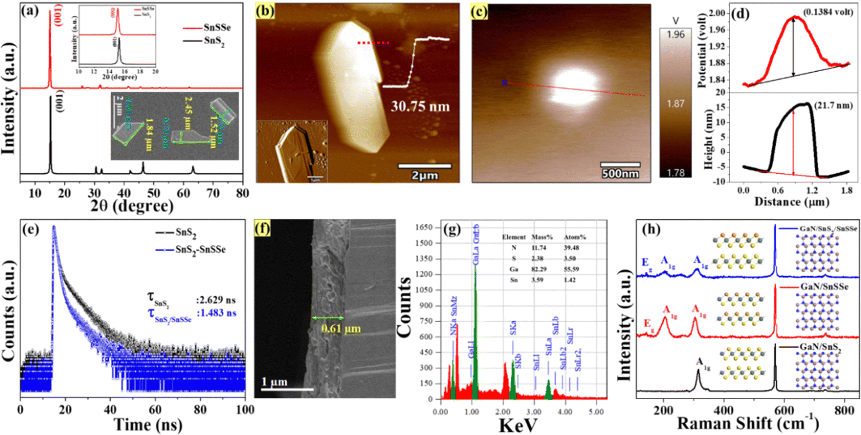 | ||
| Fig. 4 (a) XRD measurements for SnS2 and SnSSe nanosheets; inset shows FE-SEM images of SnS2 and SnSSe nanosheets. (b) Atomic force microscopy (AFM) image of SnS2, (c) Kelvin probe modes of atomic force microscopy (KP-AFM) of SnSSe nanosheet, (d) the line scan of KPFM images of 2D SnSSe nanosheets, (e) TCSPC for SnS2 and SnS2/SnSSe mixed solution, (f) cross-sectional view of FESEM of fabricated devices, (g) energy-dispersive X-ray spectroscopy (EDX) spectrum of the fabricated device, and (h) Raman spectroscopy analysis of the configured devices. | ||
Additionally, photoluminescence (PL) was employed to extract valuable insights into the optical properties of the materials, including their bandgap energy, radiative recombination processes, and defect states. This information aids in optimizing the performance of optoelectronic devices, particularly photodetectors. The PL spectra of exfoliated SnS2, excited at a wavelength of 375 nm, are illustrated in ESI,† Fig. S3(d). The spectrum reveals four distinct emission peaks observed at approximately 434 nm (violet), 460 nm (blue), 493 nm (cyan), and 520 nm (green). The most prominent emission peak occurs at 460 nm, stemming from the radiative recombination of bound excitons corresponding to a band gap of approximately 2.69 eV. This value aligns closely with the band gap calculated from the Tauc plot of the exfoliated SnS2 nanosheets, as depicted in the ESI,† Fig. S3(b).45 The PL spectrum of the SnS2 and SnSSe mixed samples under 375 nm excitation, as depicted in ESI,† Fig. S3(e), revealed significant quenching of the PL emission in the case of the mixed solution, suggesting the suppression of radiative recombination of photoinduced charge carriers by interfacial charge transfer between SnSSe and SnS2 nanosheets.46 To gain deeper insight into the photophysical processes within the heterostructure, we conducted time-resolved spectroscopic (TCSPC) measurements on both pure SnS2 and SnS2/SnSSe mixed solutions. Fig. 4(e) displays the time-resolved photoluminescence (PL) decay profiles, with excitation at 375 nm. The decay curves for all samples were fitted using a biexponential function, and the average lifetimes were determined, as illustrated in Table ST1 (ESI†). In the case of 2D SnS2, the PL decay curve features two components: (τ1) 0.914 ns (66.57%) and (τ2) 6.045 ns (33.43%). However, for 2D SnS2/SnSSe heterostructures, these components are adjusted to (τ1) 0.90 ns (86.59%) and (τ2) 5.24 ns (13.41%). Upon calculating the average lifetime (τave), it was evident that the composite of SnS2 and SnSSe nanosheets (1.483 ns) exhibits a shorter τave compared to SnS2 nanosheets (2.629 ns). This discrepancy is attributed to the shorter lifetime components (τ1), which arise due to carrier trapping in surface states (nonradiative pathways), significantly faster than the electron–hole recombination process.47 Meanwhile, the longer component (τ2) is associated with band-edge recombination of electrons at the lower level of the conduction band (CB) and valence band (VB), representing radiative pathways.48 The persistence of short lifetime components at significantly increased percentages results in substantial decreases in the average lifetimes of SnS2/SnSSe compared to SnS2. This observation strongly suggests energetic or charge transfer, or both, from SnS2 to SnSSe, which aligns with the PL quenching observed in the steady-state PL spectra shown in ESI,† Fig. S3(e). A schematic representation of the electron transfer process from SnS2 to SnSSe is depicted in ESI,† Fig. S3(f).
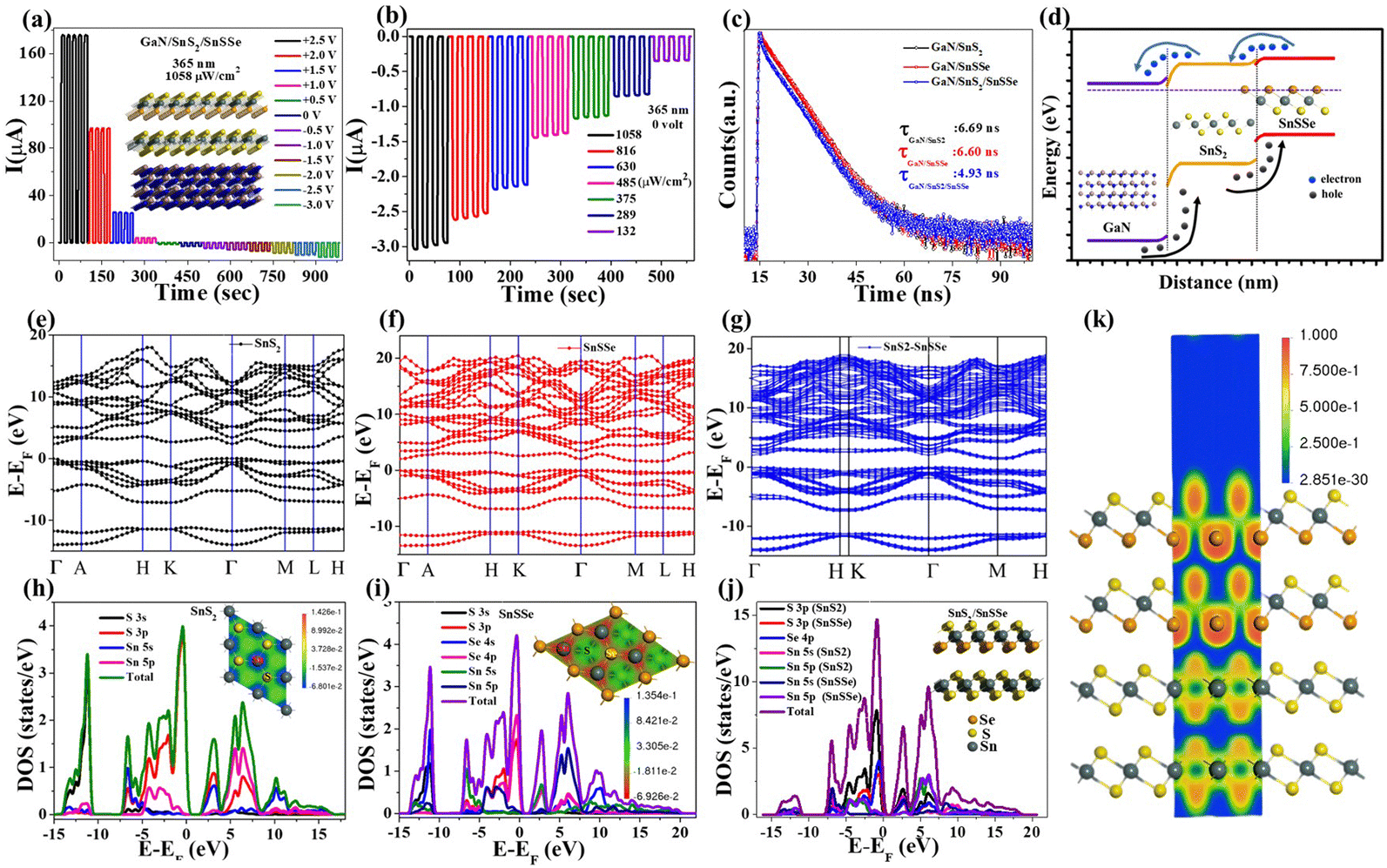
Now, using the conventional spray coating technique, three different sets of device configurations, namely D1 (GaN/SnSSe), D2 (GaN/SnS2), and D3 (GaN/SnS2/SnSSe), were fabricated on unintentionally doped GaN substrates. The thickness of the film (D2) was determined to be approximately 0.6 μm through cross-sectional view analysis using FESEM, as illustrated in Fig. 4(f). The elemental analysis was conducted using energy-dispersive X-ray spectroscopy (EDX), confirming the presence of Ga, N, Sn, and S, as depicted in Fig. 4(g). Furthermore, the configured devices underwent Raman spectroscopy analysis, as shown in Fig. 4(h). For the GaN/SnS2 device, distinct Raman active peaks were observed at 315.76 cm−1 for out-of-plane vibration modes of SnS2, along with a peak at 570.19 cm−1 corresponding to the GaN substrate.49,50 For the GaN/SnSSe device, firm peaks were observed at 304.23 cm−1 and 205 cm−1 due to out-of-plane and Raman active modes of the GaN substrate. In the case of the GaN/SnS2/SnSSe device, two out-of-plane vibration modes were identified at 314.03 cm−1 and 204.42 cm−1, along with Raman active modes of the GaN substrate, conclusively confirming the assembly of both SnS2 and SnSSe on the GaN substrates.
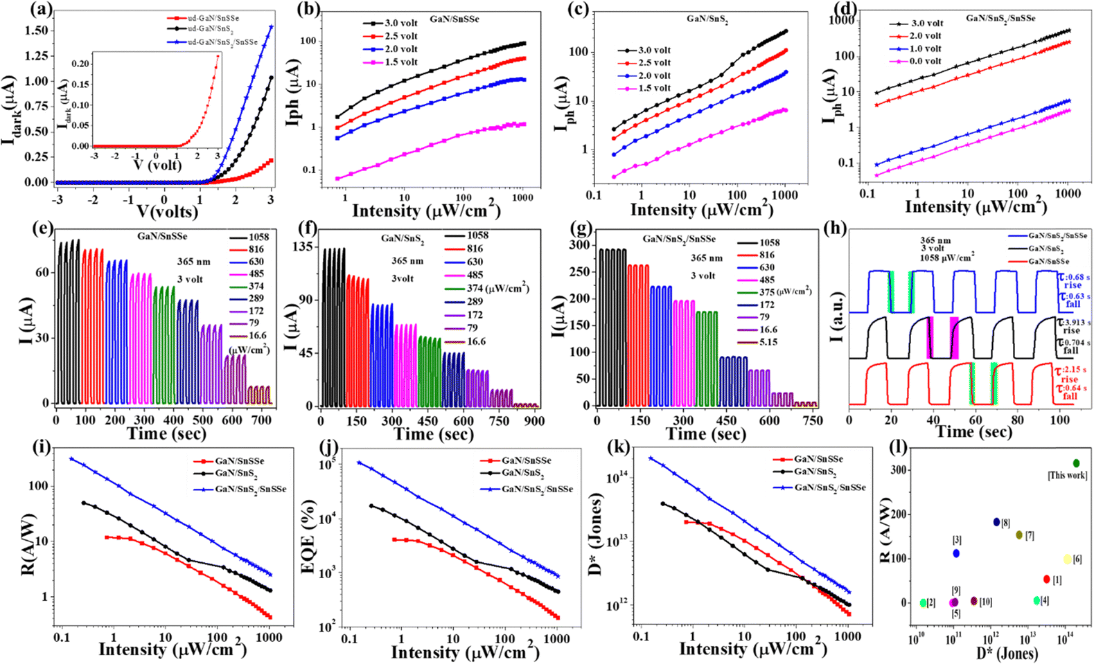
After validating the device fabrication, the electrical transport properties of the photodetector (PD) devices (D1, D2, and D3) were investigated by recording the I–V characteristics in the range of −3 V to +3 V in voltage sweeping mode. The dark I–V characteristics of these PD devices are presented in Fig. 5(a), illustrating that all the devices exhibit typical diode characteristics with well-defined rectification ratios. The dark currents recorded for devices D1, D2, and D3 at a bias of 3 V were 0.219 μA, 1.035 μA, and 1.535 μA, respectively. Fig. 5(a) demonstrates that all these PD devices show shallow leakage currents in the reverse bias and up to the cut-off bias of 2.06 eV, 1.77 eV, and 1.39 eV for devices D1, D2, and D3, respectively. The low cut-in value of D3 is suitable for low-power switching devices compared to D1 and D2 device configurations.51 ESI,† Fig. S4(a) shows the semi-logarithmic current plot as a function of voltage for all three device configurations, revealing three distinct regions with different slopes in the forward bias. The slopes of three different regions of ESI,† Fig. S4(a) for all the devices are (11.28, 2.47, 0.8: D1), (12.81, 1.62, 0.76: D2), and (3.48, 2.67, 0.48: D3) respectively. The ideality factor (n) calculated from the slope of region II of all three devices is 15.6, 23.88, and 14.49 for D1, D2, and D3, respectively. The lower (n) values for D3 indicate the lower recombination of charge carriers in regions II compared to D1 and D2. As the dark current mainly depends on the surface leakage current originating from minority charge carrier generation and poor surface passivation across the heterojunction, the dark current is higher in the case of D3 compared to D1 and D2.52–54
 | ||
| Fig. 5 (a) Dark I–V characteristics, (b)–(d) intensity-dependent photocurrent under different forward biases, (e)–(h) intensity-dependent photoswitching with a fixed bias of 3-volt, (i)–(k) intensity-dependent responsivity, EQE and specific detectivity for different devices configurations, and (l) comparison among SnS2-based hybrid heterojunction PDs. | ||
Moreover, the photoresponse of all sets of devices (with an active area of 0.2 cm2) was examined by recording the photocurrent at a 365 nm illumination wavelength with varying intensity. The dependence of the device's photocurrents on illumination intensity was investigated with different forward biases under 365 nm, as illustrated in Fig. 5(b)–(d) and in ESI,† Fig. S4(b)–(d). Given that GaN is a wide bandgap semiconductor (bandgap ∼3.4 eV), the configured devices demonstrate a well-defined photoresponse to UV (365 nm) illumination.55–57 Devices D1, D2, and D3 exhibit maximum photocurrents of 90.29 μA, 276.31 μA, and 531.95 μA, respectively, under 365 nm illumination (1058 μW cm−2) at a 3 V forward bias. The sub-linear intensity-dependent photocurrent plot indicates that all the devices can deliver significant photocurrent under very low-intensity illumination. However, only D3 can exhibit a well-defined self-powered operation, maintaining a consistent sublinear dependence of photocurrent with illumination intensity even in the absence of external bias. The photocurrent (Iph) dependency on incoming optical power is related by the equation Iph ∝ Pβ for the fabricated devices, where β is the power exponent. The β value varies in the range from 0.31 to 0.40 and 0.36 to 0.57 with forward bias (1.5–3.0 V) for D1 and D2, respectively. The gradual increase in β values with increasing forward bias discerns saturation of interface states, causing lower recombination with increasing bias for D1 and D2 device configurations.50 The power exponent value varies in the range 0.50 to 0.46 with forward bias (0–3 V) for the D3 device, clearly indicating bias-dependent recombination in the double heterojunction.
The ability for on–off switching is crucial for a good photodetector due to several reasons. Firstly, the ability to turn off the photodetector when not in use is important for conserving energy, especially in battery-operated devices where power consumption is critical.58 Secondly, strong light signals for an extended period can saturate a photodetector, leading to inaccurate readings. On–off switching helps prevent saturation by allowing the detector to “rest” or turn off when exposed to intense light, ensuring accurate measurements.59 To assess the stability and repeatability of the fabricated devices, time-dependent photocurrent measurements were conducted, as depicted in Fig. 5(e)–(h). These figures illustrate the time-dependent photocurrent of devices D1, D2, and D3 under 365 nm illumination with varying intensities at a fixed bias of 3 volts. Device D1 demonstrates a photoresponse enhancement from 7.78 μA to 73.9 μA as the illumination intensity increases from 16.6 μW cm−2 to 1058 μW cm−2. Similar time-dependent photoresponse characteristics were observed for both D2 and D3. Specifically, D2 exhibits a photoresponse enhancement from 2.01 μA to 133.9 μA as the illumination intensity increases from 16.6 μW cm−2 to 1058 μW cm−2. Notably, the time-dependent photocurrent of D3, as shown in Fig. 5(g), exhibited a maximum photoresponse of 292.2 μA (1058 μW cm−2), which is equivalent to 3.95- and 2.18-time maximum photoresponse of D1 and D2, respectively. To determine the switching speed of the fabricated devices, the normalized time-dependent photoresponse under 365 nm illumination with a fixed bias of 3 volts was plotted, as depicted in Fig. 5(h). The rise time (τrise) and fall time (τfall) of the fabricated devices are as follows: (2.15 s, 3.913 s) for D1, (0.64 s, 0.7 s) for D2, and (0.686 s, 0.639 s) for D3. The quick rise time of D3 demonstrates evident binary photoresponse characteristics with smooth photo carrier channelling for efficient photodetector application.
Furthermore, to evaluate the PD performance of both devices, we estimated three important parameters, viz. responsivity 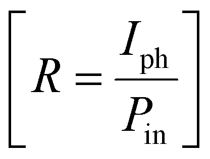 , specific detectivity
  , and external quantum efficiency
  , where Iph, Pin, A, and Idark are photocurrent, the incident optical power, active area of PDs and dark current of the device, respectively.60 The photoresponsivity (R), external quantum efficiency (EQE), and specific detectivity (D*) under 365 nm illumination as a function of illumination intensity at a fixed forward bias of 3 volts for the fabricated devices are presented in Fig. 5(i)–(k). R and EQE maintain a sub-linear dependence with increasing illumination intensity, signifying consistent photodetection over comprehensive intensity regimes. The highest recorded responsivity values for the fabricated devices at a fixed bias are 314.96 A W−1, 50.34 A W−1, and 11.98 A W−1 for D1, D2, and D3, respectively. Despite D1 exhibiting shallow dark current (0.219 μA) compared to D2 (1.035 μA), D2 shows much higher photocurrent than D1 in the intensity range of 220–1058 μW cm−2, resulting in higher specific detectivity values for D2 within the same intensity range. Given that the photocurrent of D3 surpasses that of D1 and D2 throughout the intensity range and maintains sub-linear dependency of specific detectivity, the highest recorded specific detectivity values are 2.02 × 10¹³ jones, 3.91 × 10¹³ jones, and 2.0 × 10¹⁴ jones, respectively, for the device configurations D1, D2, and D3 under 365 nm illumination with a fixed bias of 3 volts. Furthermore, we conducted a comparative analysis of our current study with other experimental investigations focused on SnS2-based UV photodetectors. The photodetection parameters extracted from these studies are tabulated in ESI,† Table ST3, while Fig. 5(l) illustrates a graphical representation of the comparison. In Table 1, we present the highest recorded photodetection parameters across various device types under 365 nm illumination with a bias of 3 volts. This comparison provides valuable insights into the performance of our fabricated devices relative to existing research endeavours in the field of SnS2-based UV photodetection.
| Device ID | Structure | IDark (μA) | R (A W−1) | D (jones) | EQE (%) |
|---|---|---|---|---|---|
| D 1 | GaN/SnSSe | 0.219 | 11.98 | 2.02 × 10¹³ | 4.07 × 10³ |
| D 2 | GaN/SnS2 | 1.035 | 50.34 | 3.91 × 10¹³ | 1.71 × 10⁴ |
| D 3 | GaN/SnS2/SnSSe | 1.535 | 314.96 | 2.0 × 10¹⁴ | 10.7 × 10⁴ |
To assess the stability and repeatability of the fabricated devices, we conducted time-dependent photocurrent measurements with varying the bias while maintaining a constant intensity of 1058 μW cm−2, as illustrated in ESI,† Fig. S4(e) and (f) and Fig. 6(a). Consistent time-dependent photoresponse characteristics were observed for devices D1 and D2, as depicted in ESI,† Fig. S4(e) and 4(f). For the D1 and D2 devices, the time-dependent photoresponse ranged from 1.17 μA to 73.9 μA and from 2.76 μA to 133.9 μA, respectively, with the applied forward bias ranging from 1.5 volts to 3.0 volts under 365 nm illumination (fixed intensity: 1058 μW cm−2). Notably, device D3 exhibited bias-dependent photoswitching behavior across the range from +3 volts to −3 volts. The amplitude of the photoresponse increased from 3.03 μA to 292.2 μA and from 3.03 μA to 12.2 μA as the bias varied from 0 volts to +3 volts and 0 volts to −3 volts, respectively, for D3, with a fixed intensity of 1058 μW cm−2, as depicted in Fig. 6(a). Furthermore, to validate the self-powered operation of D3, intensity-dependent photoswitching without any bias was investigated, as shown in Fig. 6(b). The proportional enhancement of the photocurrent from 0.33 μA to 3.03 μA with increasing intensity from 132 μW cm−2 to 1058 μW cm−2 indicates the self-powered mode of the D3 device configuration. Now, the intensity-dependent photocurrent plot shown in Fig. 5(d) for the D3 device configuration indicates that the device can deliver significant photocurrent (45.8 nA to 3.03 μA) by varying the illumination intensity from 0.15 to 1058 μW cm−2. Consequently, our fabricated device D3 is able to show maximum R, EQE (%) and D* as 1.52 A W−1, 519.3% and 6.06 × 10¹³ jones under the illumination of 365 nm with a low intensity of 150 nW cm−2 without any external bias, i.e. in self-powered mode.
 | ||
| Fig. 6 (a) Bias-dependent photoswitching with a fixed intensity of 1058 μW cm−2 for the D3 device configuration, (b) intensity-dependent photoswitching without any bias (0 volt) for the D3 device configuration, (c) TCSPC for different device configurations under 375 nm excitation, (d) schematics of the energy band diagram for the D3 device configuration, (e)–(g) simulated band structures for SnS2, SnSSe, and SnS2/SnSSe, respectively, (h)–(j) density of states (DOS) for SnS2, SnSSe, and SnS2/SnSSe, respectively, and (k) electron localization function for the D3 device configuration. | ||
To investigate the charge transport mechanism of our fabricated heterojunctions, we conducted time-resolved photoluminescence (TCSPC) experiments. The photoluminescence decay profiles of these heterojunctions under excitation (375 nm) and recorded emission (460 nm) are presented in Fig. 6(c). We performed bi-exponential fitting of the PL decay curves and recorded average lifetimes, which are tabulated in ESI,† Table ST2. The luminescence decay profiles consist of two decay components: τ1 (short lifetime, nonradiative decay component) and τ2 (long lifetime, radiative component). We observed a considerable enhancement in the amplitude of the nonradiative decay component τ1 for D3 (36.69%) compared to D1 (9.39%) and D2 (9.76%) heterojunctions, with a slight increase in decay time. In contrast, the radiative decay component τ2 showed almost no change in decay time but exhibited significant decreases in relative amplitude. Overall, the average decay lifetimes of D1 and D2 are 6.603 ns and 6.692 ns, respectively, drastically reduced to 4.931 ns for D3. This drastic reduction in the average decay lifetime of D3 indicates efficient interfacial carrier transfer through SnS2, with a rate constant (Kct) of 5.135 × 10⁷ s−1.61,62 This enhanced carrier transport through SnS2 from photoexcited SnSSe results in higher photocurrent in switching characteristics with fast rise and decay time observed in the D3 device configuration, as demonstrated in Fig. 5(g) and (h).
To gain further insight, we constructed schematic energy band diagrams for D1, D2, and D3, considering the band positions illustrated in ESI,† Fig. S5(a), (b), and Fig. 6(d). The band gaps of bulk SnS2 and SnSSe were calculated to be 2.18 eV and 1.7 eV, respectively, from the Tauc plot of the absorption spectrum, as shown in ESI,† Fig. S3(a). The bandgap of GaN was taken as 3.4 eV based on reported data. The electron affinities of GaN, SnS2, and SnSSe were considered as −4.1 eV, −4.16 eV, and −4.3 eV, respectively.63,64 The conduction band offset and valence band offset for D1 and D2 were calculated as follows: ΔEc1: −0.2 eV, ΔEv1: 1.5 eV, and ΔEc2: −0.06 eV, ΔEv2: 1.16 eV, with effective built-in potentials of −0.8 eV and −0.6 eV, respectively. This calculation took into account the work function values of GaN, SnS2, and SnSSe as 4.2 eV, 4.8 eV, and 5.0 eV, respectively. D1 and D2 demonstrate single type-II heterostructures between SnSSe and SnS2 with GaN, facilitating efficient charge transport for photodetector applications. On the other hand, D3 exhibits two favorable type-II band alignments (staircase) at the GaN–SnS2 and SnS2/SnSSe interfaces, making it superior for photodetector application. An additional valence band can enable more efficient hole transport within the heterostructures (D3), potentially reducing the likelihood of recombination and improving overall device performance. The combination of different materials in a van der Waals heterostructure (D3) can lead to synergistic effects not present in the individual heterojunctions (D1 and D2). These effects could involve a combination of band alignment, electronic structure modifications, and interface effects, all contributing to an increased effective built-in potential for D3. Under the influence of this built-in potential, photogenerated carriers can efficiently separate even in the absence of external bias (self-powered mode).
DFT simulations were conducted to elucidate the mechanism of charge transport between SnS2 and SnSSe. The BFGS algorithm, utilizing a quadratic potential to determine an optimal step length per iteration, was employed for the geometry optimization of these structures.65 The electronic band gaps of bulk SnS2, SnSSe, and their heterostructure were simulated using the discussed methods. The calculated band gaps for bulk SnS2, SnSSe, and the SnS2/SnSSe heterostructure were estimated to be 1.8 eV, 1.55 eV, and 1.4 eV, respectively. The band structures were computed along specific high-symmetry points: Γ (0,0,0) → A (0,0,0.5) → H (−0.333,0.667,0.5) → K (−0.333,0.667,0) → Γ (0,0,0) → M (0,0.5,0) → L (0,0.5,0.5) → H (−0.333,0.667,0.5), as illustrated in Fig. 6(e)–(g).66 These structures exhibit typical indirect bandgap characteristics consistent with reported findings. The projected density of states (PDOS) of SnS2, depicted in Fig. 6(h), reveals strong hybridization in the valence band between the 5p states of Sn-atoms and 3p states of S-atoms. The conduction band is influenced by the hybridization between 3p states of S-atoms and 5s,5p states of Sn-atoms. Fig. 6(h) also presents the electron density difference (EDD) plot for SnS2 (top view). In contrast, the valence band of SnSSe primarily depends on the 4p states of Se-atoms, 3p states of S atoms, and 5p states of Sn-atoms, while the conduction band strongly relies on the 5s states of Sn-atoms and 4p states of Se-atoms, as depicted in Fig. 6(i).
Furthermore, the charge distribution of different species in both SnS2 and SnSSe was investigated through Mullikan and Hirshfeld population analysis, as tabulated in ESI,† Tables ST4 and ST5. According to the Hirshfeld population analysis, bulk SnS2 indicates Hirshfeld charges of 0.28e for Sn atoms and −0.14e for S atoms. In comparison, for SnSSe, the Hirshfeld charges are 0.26e for Sn atoms, −0.15e for S atoms, and −0.11e for Se atoms. The band structures of SnS2/SnSSe were computed along the same high symmetry points demonstrated in Fig. 6(g). The simulated band structure exhibits typical characteristics of an indirect bandgap with significantly reduced bandgap values. This reduction is attributed to balanced band structures with a uniform Fermi level and Bader charge transfer effect, through which electrons and holes contribute to shifting the conduction and valence bands, facilitating efficient photogenerated charge carrier transportation.67 The total and projected density of states for SnS2/SnSSe heterostructures are depicted in Fig. 6(j). From this plot, it is observed that the valence band maxima mainly depend on the strong hybridization of 3p states of S atoms from both SnS2 and SnSSe with 4p states of Se atoms (from SnSSe), while the conduction band comprises mainly S 3p states (from SnS2), Sn 5s states (from SnS2), and Sn 5s states (from SnSSe). To better understand charge transfer in the heterostructure, the electron localization function (ELF) and electron density difference (EDD) map of the SnS2/SnSSe heterostructure were calculated, as displayed in Fig. 6(k) and ESI,† Fig. S5(c). The Mullikan and Hirshfeld population analysis of the SnS2/SnSSe heterostructure interface indicates that Sn atoms (in SnS2) and S atoms (in SnS2) have Hirshfeld charges of 0.29e and −0.14e, respectively, while Sn atoms (in SnSSe), S atoms (in SnSSe), and Se atoms (in SnSSe) have Hirshfeld charges of 0.25e, −0.15e, and −0.11e, respectively, as tabulated in ESI,† Table ST6. This suggests that Sn atoms (in SnSSe) gain more electrons than Sn atoms (in SnS2), facilitating efficient electron transfer at the interface. Furthermore, the electron localization function of the SnS2/SnSSe heterostructure clearly demonstrates that electron localization gradually decreases from SnSSe to SnS2, indicating efficient charge transfer in the SnS2/SnSSe heterostructure for photodetector applications, as displayed in Fig. 6(k).
4. Conclusion
In conclusion, this study introduces a pioneering approach for synthesizing highly crystalline SnSSe alloy resembling Janus structures, achieved through solvothermal synthesis, marking a notable advancement in the field. The study's significant contribution lies in elucidating the charge transfer dynamics between SnS2 and SnSSe, supported by PL quenching, TCSPC, and DFT investigations, laying the foundation for designing efficient photodetectors. Through precise spray-coating, three distinct devices, namely, GaN/SnSSe (D1), GaN/SnS2 (D2), and GaN/SnS2/SnSSe (D3), are fabricated, resulting in notable enhancements in photodetection capabilities. In particular, the double heterojunction (GaN/SnS2/SnSSe) with a staircase-like (type-II) band alignment demonstrates significantly enhanced photodetection capabilities compared to single heterojunction counterparts, amplifying light absorption and enabling effective electron–hole pair separation. Insights from time-resolved spectroscopic measurements provide clarity on photophysical mechanisms within the heterostructure, indicating efficient charge transfer between constituent materials. The photodetector exhibits a high photoresponsivity of 314.96 A W−1, specific detectivity of 2.0 × 10¹⁴ jones, and external quantum efficiency of 10.7 × 10⁴% under 365 nm illumination at an intensity of 150 nW cm−2 and a bias of 3 V. Remarkably, D3 demonstrates well-defined intensity-dependent photocurrent and photo switching even without external bias, showcasing its self-powered mode. Under low intensity and without external bias, D3 achieves maximum responsivity (1.52 A W−1), external quantum efficiency (519.3%), and detectivity (6.06 × 10¹³ jones). Overall, the successful integration of SnS2 and SnSSe in a van der Waals heterostructure on a GaN platform for self-powered UV photodetection signifies a significant leap in optoelectronics. The exploration of tin dichalcogenides, particularly SnSSe, continues to unlock new possibilities for high-performance optoelectronic devices with broad applications.Conflicts of interest
There are no conflicts to declare.Acknowledgements
PK acknowledges financial support from the Science and Engineering Research Board (grant no. CRG/2023/000092), Department of Atomic Energy “58/14/14/2023-BRNS/12280”. SM acknowledges CSIR for its financial support in the form of a JRF Fellowship (09/080(1145)/2020-EMR-I).References
- W. Ahmad, J. Wu, Q. Zhuang, A. Neogi and Z. Wang, Small, 2023, 19, 2207641 CrossRef CAS PubMed
.
- R. Dutta, A. Bala, A. Sen, M. R. Spinazze, H. Park, W. Choi, Y. Yoon and S. Kim, Adv. Mater., 2023, 35, 2303272 CrossRef CAS PubMed
- Y. Jing, B. Liu, X. Zhu, F. Ouyang, J. Sun and Y. Zhou, Nanophotonics, 2020, 9, 1675–1694 CrossRef CAS
- Q. Zeng and Z. Liu, Adv. Electron. Mater., 2018, 4, 1700335 CrossRef
- C. Gong, Y. Zhang, W. Chen, J. Chu, T. Lei, J. Pu, L. Dai, C. Wu, Y. Cheng, T. Zhai, L. Li and J. Xiong, Adv. Sci., 2017, 4, 1700231 CrossRef
- Y. Peng, J. Hu, Y. Huan and Y. Zhang, Nanoscale, 2024, 16, 7734–7751 RSC
- A. Chaves, J. G. Azadani, H. Alsalman, D. R. da Costa, R. Frisenda, A. J. Chaves, S. H. Song, Y. D. Kim, D. He, J. Zhou, A. Castellanos-Gomez, F. M. Peeters, Z. Liu, C. L. Hinkle, S. H. Oh, P. D. Ye, S. J. Koester, Y. H. Lee, P. Avouris, X. Wang and T. Low, npj 2D Mater. Appl., 2020, 4, 1–21 CrossRef
- X. Yao, Y. Wang, X. Lang, Y. Zhu and Q. Jiang, Phys. E, 2019, 109, 11–16 CrossRef CAS
- M. Chen, J. Chai, J. Wu, H. Zheng, W. Y. Wu, J. Lourembam, M. Lin, J. Y. Kim, J. Kim, K. W. Ang, M. F. Ng, H. Medina, S. W. Tong and D. Chi, Nanoscale Horiz., 2023, 9, 132–142 RSC
- S. Li, X. Liu, H. Yang, H. Zhu and X. Fang, Nat. Electron., 2024, 7, 216–224 CrossRef CAS
- T. Chen, Q. Feng, W. Feng and X. Yang, J. Alloys Compd., 2024, 971, 172657 CrossRef CAS
- J. Jiang, J. Huang, Z. Ye, S. Ruan and Y. J. Zeng, Adv. Mater. Interfaces, 2020, 7, 2000882 CrossRef CAS
- S. Deng, Y. Chen, Q. Li, J. Sun, Z. Lei, P. Hu, Z. Liu, X. He and R. Ma, Nanoscale, 2022, 14, 14097–14105 RSC
- Y. Zhao, T. Y. Tsai, G. Wu, C. Ó. Coileáin, Y. F. Zhao, D. Zhang, K. M. Hung, C. R. Chang, Y. R. Wu and H. C. Wu, ACS Appl. Mater. Interfaces, 2021, 13, 47198–47207 CrossRef CAS
- Q. Yue, W. Gao, P. Wen, Q. Chen, M. Yang, Z. Zheng, D. Luo, N. Huo, F. Zhang and J. Li, J. Mater. Chem. C, 2021, 9, 15662–15670 RSC
- J. Yu, A. A. Suleiman, Z. Zheng, X. Zhou and T. Zhai, Adv. Funct. Mater., 2020, 30, 2001650 CrossRef CAS
- L. Du, C. Wang, W. Xiong, B. Wei, F. Yang, S. Chen, L. Ma, X. Wang, C. Xia, X. Zhang, Z. Wang and Q. Liu, Adv. Mater. Technol., 2020, 5, 1900853 CrossRef CAS
- P. Perumal, R. K. Ulaganathan, R. Sankar, Y. M. Liao, T. M. Sun, M. W. Chu, F. C. Chou, Y. T. Chen, M. H. Shih and Y. F. Chen, Adv. Funct. Mater., 2016, 26, 3630–3638 CrossRef CAS
- X. Wang, D. Chen, Z. Yang, X. Zhang, C. Wang, J. Chen, X. Zhang and M. Xue, Adv. Mater., 2016, 28, 8645–8650 CrossRef CAS PubMed
- Y. Zhang, J. Yang, Y. Zhang, C. Li, W. Huang, Q. Yan and X. Dong, ACS Appl. Mater. Interfaces, 2018, 10, 12722–12730 CrossRef CAS PubMed
- W. Zhang, J. Zhang, C. He and T. Li, Int. J. Energy Res., 2022, 46, 267–277 CrossRef CAS
- C. Fan, Y. Li, F. Lu, H. X. Deng, Z. Wei and J. Li, RSC Adv., 2016, 6, 422–427 RSC
- P. Tripathi, A. Kumar, P. K. Bankar, K. Singh and B. K. Gupta, Crystals, 2023, 13, 1131 CrossRef CAS
- J. Chen, M. Liu, X. Liu, Y. Ouyang, W. Liu and Z. Wei, Nanophotonics, 2020, 9, 2549–2555 CrossRef CAS
- M. Usman, Z. Muhammad, G. Dastgeer, N. Zawadzka, Y. Niu, M. Imran, M. R. Molas and H. Rui, Inorg. Chem. Front., 2022, 9, 294–301 RSC
- W. Liu, Y. Yu, M. Peng, Z. Zheng, P. Jian, Y. Wang, Y. Zou, Y. Zhao, F. Wang, F. Wu, C. Chen, J. Dai, P. Wang and W. Hu, InfoMat, 2023, 5, 1–31 Search PubMed
- J. Xu, H. Zhang, Z. Song, Y. Xu, Q. Peng, X. Xiu, Z. Li, C. Li, M. Liu and B. Man, Appl. Surf. Sci., 2020, 506, 144671 CrossRef CAS
- J. Y. Lee, J. H. Shin, G. H. Lee and C. H. Lee, Nanomaterials, 2016, 6, 193 CrossRef PubMed
- W. Liao, Y. Huang, H. Wang and H. Zhang, Appl. Mater. Today, 2019, 16, 435–455 CrossRef
- A. Li, Q. Chen, P. Wang, Y. Gan, T. Qi, P. Wang, F. Tang, J. Z. Wu, R. Chen, L. Zhang and Y. Gong, Adv. Mater., 2019, 31, 1805656 CrossRef
- M. Kumar, B. R. Huang, A. Saravanan, H. Sun and S. C. Chen, Adv. Electron. Mater., 2024, 10, 2400164 CrossRef
- H. Wang, Y. Wang, X. Li, X. Liu, X. Zheng, Y. Shi, M. Xu, J. Zhang and Q. Zhang, J. Alloys Compd., 2022, 920, 165974 CrossRef CAS
- Y. Yan, J. Li, H. Li, S. Li, Z. Li, W. Gao, Y. Jiang, X. Song, C. Xia and J. Li, Appl. Phys. Lett., 2023, 122, 043505 CrossRef CAS
- S. Abbas, D. K. Ban and J. Kim, Sens. Actuators, A, 2019, 293, 215–221 CrossRef CAS
- S. J. ClarkI, M. D. Segall II, C. J. Pickard II, P. J. Hasnip III and M. I. J. Probert IV, Z. Kristallogr., 2005, 220, 567–570 Search PubMed
- L. Deng, H. Liu, X. Gao, X. Su and Z. Zhu, Ceram. Int., 2016, 42, 3808–3815 CrossRef CAS
- Y. Fu, G. Gou, X. Wang, Y. Chen, Q. Wan, J. Sun, S. Xiao, H. Huang, J. Yang and G. Dai, Appl. Phys. A: Mater. Sci. Process., 2017, 123, 299 CrossRef
- X. Xiong, J. Zhang, C. Chen, S. Yang, J. Lin, J. Zeng, J. Xi, Z. Kong and Y. J. Yuan, J. Alloys Compd., 2022, 911, 165106 CrossRef CAS
- E. Huang, X. Yao, W. Wang, G. Wu, N. Guan and L. Li, ChemPhotoChem, 2017, 1, 60–69 CrossRef CAS
- A. K. Garg, J. Mol. Struct., 1991, 247, 47–60 CrossRef CAS
- L. Huang, G. Cai, R. Zeng, Z. Yu and D. Tang, Anal. Chem., 2022, 94, 9487–9495 CrossRef CAS PubMed
- L. Shooshtari, A. Esfandiar, Y. Orooji, M. Samadpour and R. Rahighi, Sci. Rep., 2021, 11, 19353 CrossRef CAS PubMed
- A. Sierra-Castillo, E. Haye, S. Acosta, R. Arenal, C. Bittencourt and J. F. Colomer, RSC Adv., 2021, 11, 36483–36493 RSC
- L. Wu, W. Gao, Y. Sun, M. M. Yang, Z. Zheng, W. Fan, K. Shu, Z. Dan, N. Zhang, N. Huo and J. Li, Adv. Mater. Interfaces, 2022, 9, 2102099 CrossRef CAS
- S. Das, K. J. Sarkar, B. Pal, H. Mondal, S. Pal, R. Basori and P. Banerji, J. Appl. Phys., 2021, 129, 053105 CrossRef CAS
- R. Zhang, L. Bi, D. Wang, Y. Lin, X. Zou, T. Xie and Z. Li, J. Colloid Interface Sci., 2020, 578, 431–440 CrossRef CAS PubMed
- H. Cheng, Y. Feng, Y. Fu, Y. Zheng, Y. Shao and Y. Bai, J. Mater. Chem. C, 2022, 10, 13590–13610 RSC
- S. Maity, K. Sarkar and P. Kumar, Nanoscale, 2023, 15, 16068–16079 RSC
- H. Ying, X. Li, Y. Wu, Y. Yao, J. Xi, W. Su, C. Jin, M. Xu, Z. He and Q. Zhang, Nanoscale Adv., 2019, 1, 3973–3979 RSC
- S. Maity, K. Sarkar and P. Kumar, ACS Appl. Nano Mater., 2023, 6, 4224–4235 CrossRef CAS
- M. Tyagi, M. Tomar and V. Gupta, Mater. Res. Bull., 2015, 66, 123–131 CrossRef CAS
- R. Peng, S. Jiao, D. Jiang, H. Li and L. Zhao, Thin Solid Films, 2017, 629, 55–59 CrossRef CAS
- X. Du, G. R. Savich, B. T. Marozas and G. W. Wicks, J. Electron. Mater., 2018, 47, 1038–1044 CrossRef CAS
- H. J. Song, C. H. Roh, J. H. Lee, H. G. Choi, D. H. Kim, J. H. Park and C. K. Hahn, Semicond. Sci. Technol., 2009, 24, 065003 CrossRef
- Z. Fan, IOP Conf. Ser. Mater. Sci. Eng., 2020, 738, 012006 CrossRef CAS
- N. Aggarwal and G. Gupta, J. Mater. Chem. C, 2020, 8, 12348–12354 RSC
- L. Goswami, N. Aggarwal, P. Vashishtha, S. K. Jain, S. Nirantar, J. Ahmed, M. A. M. Khan, R. Pandey and G. Gupta, Sci. Rep., 2021, 11, 10859 CrossRef CAS PubMed
- L. Peng, L. Hu and X. Fang, Adv. Funct. Mater., 2014, 24, 2591–2610 CrossRef CAS
- G. W. Anderson, B. D. Guenther, J. A. Hynecek, R. J. Keyes and A. VanderLugt, Appl. Opt., 1988, 27, 2871–2886 CrossRef CAS PubMed
- S. Maity, K. Sarkar and P. Kumar, J. Mater. Chem. C, 2021, 9, 14532–14572 RSC
- R. A. Scheidt, E. Kerns and P. V. Kamat, J. Phys. Chem. Lett., 2018, 9, 5962–5969 CrossRef CAS PubMed
- C. W. Tsao, M. J. Fang and Y. J. Hsu, Coord. Chem. Rev., 2021, 438, 213876 CrossRef CAS
- K. Sarkar, M. Hossain, P. Devi, K. D. M. Rao and P. Kumar, Adv. Mater. Interfaces, 2019, 6, 1900923 CrossRef CAS
- L. A. Burton, T. J. Whittles, D. Hesp, W. M. Linhart, J. M. Skelton, B. Hou, R. F. Webster, G. O’Dowd, C. Reece, D. Cherns, D. J. Fermin, T. D. Veal, V. R. Dhanak and A. Walsh, J. Mater. Chem. A, 2016, 4, 1312–1318 RSC
- B. G. Pfrommer, M. Cote, S. G. Louie and M. L. Cohen, J. Comput. Phys., 1997, 131, 233–240 CrossRef CAS
- L. Sun, W. Zhou, Y. Liu, D. Yu, Y. Liang and P. Wu, RSC Adv., 2016, 6, 3480–3486 RSC
- S. Xia, Y. Diao and C. Kan, J. Colloid Interface Sci., 2022, 607, 913–921 CrossRef CAS PubMed
Footnote |
| † Electronic supplementary information (ESI) available. See DOI: https://doi.org/10.1039/d4nh00102h |
| This journal is © The Royal Society of Chemistry 2024 |