 Open Access Article
Creative Commons Attribution 3.0 Unported Licence
Cluster-doping in silicon nanocrystals†
Atta ul
Haq
a,
Marius
Buerkle
b,
Bruno
Alessi
b,
Vladimir
Svrcek
b,
Paul
Maguire
 a and
Davide
Mariotti
 *c
*c
aSchool of Engineering, Ulster University, York Street, Belfast BT15 1ED, UK
bRenewable Energy Research Center, National Institute of Advanced Industrial Science and Technology (AIST), Tsukuba, Ibaraki 305-8568, Japan
cDepartment of Design, Manufacturing & Engineering Management, University of Strathclyde, Glasgow, UK. E-mail: davide.mariotti@strath.ac.uk
First published on 29th August 2024
Abstract
Creating tin-alloyed silicon nanocrystals with tailored bandgap values is a significant challenge, primarily because a substantial concentration of tin is essential to observe useful changes in the electronic structure. However, high concentration of Sn leads to instability of the silicon–tin nanocrystals. This work introduces a completely new approach to doping and the modification of the electronic structure of nanoparticles by incorporating few-atom clusters in nanocrystals, deviating from isolated atom doping or attempting alloying. This approach is exemplified via a combined theoretical and experimental study on tin (Sn) ‘cluster-doping’ of silicon (Si) nanocrystals, motivated by the opportunities offered by the Si–Sn system with tailored band energy. First-principles modelling predicts two noteworthy outcomes: a considerably smaller bandgap of these nanocrystals even with a modest concentration of tin compared to an equivalent-sized pure silicon nanocrystal and an unexpected decrease in the bandgap of nanocrystals as the diameter of nanocrystals increases, contrary to the typical quantum confined behaviour. Experimental verification using atmospheric pressure microplasma synthesis confirms the stability of these nanocrystals under ambient conditions. The plasma-synthesised nanocrystals exhibited the predicted atypical size-dependent behaviour of the bandgap, which ranged from 1.6 eV for 1.4 nm mean diameter particles to 2.4 eV for 2.2 nm mean diameter particles.
New conceptsDoping has been a long standing and highly successful approach to the manipulation of materials properties bringing great technological progress and superior device performance in many disciplines. We present here our work that breaks through boundaries into a novel realm of possibilities through ‘cluster doping’. We present, both theoretically and experimentally, the possibility of introducing doping elements in clusters and demonstrate that this approach largely differs from a distributed doping of single atoms, producing a manipulation of the energy band structure not achievable otherwise. Cluster-doping represents a completely novel approach that has become possible only thanks to most recent progress in the understanding of ultra-small particulates, i.e. clusters, and thanks to the development of the required synthesis and characterization capabilities. Our work delivers a completely new unexplored avenue that will impact future work in physics, chemistry and biology as cluster-doping can achieve unprecedented materials manipulation. In our manuscript we cover the fundamental aspects of synthesis, structure, composition, and properties stemming from cluster-doping providing an important view of its technological ends and specifically for solar energy conversion, with consequential great influence on the development of society in the years to come. |
1. Introduction
Nanocrystals with tailored electronic and structural characteristics present a significant potential across a broad spectrum of applications, encompassing the electrical, optical, and biomedical domains. In recent years, various types of nanocrystals have been successfully fabricated, each displaying distinctive properties, thus expanding the portfolio of available materials for device engineering.1–11 Doping and alloying in bulk materials have represented an indispensable tool for application devices and much work has been carried out, for instance to provide doping strategies for nanocrystals and quantum dots.12–15 In some cases, however, nanocrystal doping has exhibited limitations due to solubility and structural stability constraints, which can prevent the intended results.1,16–19 These issues necessitate an innovative approach to circumvent the associated restraints.Alloying silicon nanocrystals with tin, for instance, offers a powerful tool to modulate electronic properties through varying Sn doping concentration while ensuring the stability beyond conventional silicon processing temperatures.20–23 Theoretical studies have shed light on the exceptional characteristics of the Si–Sn system. It has been reported that with an increase in Sn concentration, the bandgap of Si nanocrystals decreases.23–25 This relationship is particularly important for photovoltaic applications, where nanocrystals operating within the strong quantum confinement regime can dramatically enhance carrier multiplication, a prerequisite for high-efficiency solar cells with a target bandgap range of 0.6 eV to 1 eV.26
Despite the promising prospects, however, maintaining strong quantum confinement often results in bandgap values that significantly exceed the ideal range. Although doping theoretically enables the simultaneous reduction of the bandgap and preservation of the quantum confinement regime, achieving this balance requires Sn concentrations that are notably high, posing substantial challenges.23 To date, the highest Sn concentration reported in experimental studies stands at approximately 17%, which is insufficient to generate narrow bandgap nanocrystals or to induce a fundamental gap with a direct transition.22 Additionally, increasing Sn concentration introduces instability into the Si–Sn system due to the positive enthalpy associated with the immiscibility of Si and Sn.27,28
However, bulk theoretical studies have shown that the expectation of a random solid solution in the SiSn system should be challenged and that a strong short-range order is favourable with significant changes in the SiSn electronic structure.29 The driving force of this short-range order is the competition between repulsive forces between Sn atom coordination and we can expect that in geometrically confined systems such as nanocrystals, such forces may lead to unexpected arrangements involving the nanocrystal surface with an increased freedom of structure relaxation and formation of surface states.
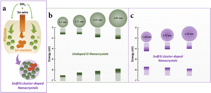
In this study, we propose a unique and innovative approach, incorporating small clusters of Sn atoms into the silicon nanocrystals, i.e. ‘cluster doping’, as opposed to uniformly distributed but isolated Sn atoms in Si nanocrystals as would be expected in an alloyed or doped system. First-principles simulations reveal that such a configuration, even at relatively low tin concentrations, can yield bandgaps with values substantially lower than that of pure silicon. Interestingly, in contrast to expected quantum confinement behaviour, a decrease in bandgap is observed with decreasing nanocrystal size.
Experimentally, we achieved synthesis with an atmospheric pressure microplasma.30 Theoretical calculations corroborated by a combination of material characterization and analytical techniques have confirmed that the total number of incorporated Sn atoms remains nearly constant regardless of the size of the nanocrystals synthesized; hence the Sn concentration decreases with increasing nanocrystal diameter. Furthermore, the bandgap value and its size-dependency observed experimentally agree with our theoretical predictions.
2. Results and discussion
2.1 Theoretical calculations of Sn cluster-doped Si NCs
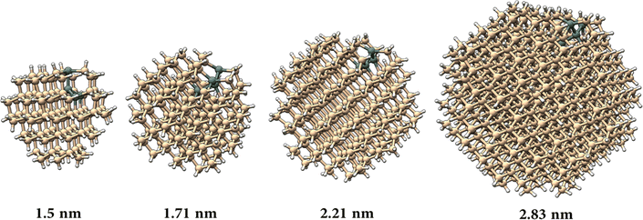
To model the nanocrystal geometry with Sn cluster doping, we generate an initial structure with the desired radius (origin at a silicon atom) cut out from the corresponding silicon bulk lattice (diamond cubic lattice, a = 0.54 nm) with under-coordinated surface atoms removed, and fully passivated by hydrogen. To identify the tin substitution sites, we start by calculating all possible fully optimized structures where a single Si atom is replaced by Sn using M3GNet neural network potentials.31 We select the energetically most favourable geometry and repeat this process until the desired Sn concentration is achieved, here 4 Sn atoms. We consider 4 Si nanocrystals (NCs) with increasing diameter d, i.e., d = 1.50 nm, d = 1.71 nm, d = 2.21 nm and d = 2.83 nm.The obtained structures are summarized in Fig. 1 and, for all the four NCs with different diameters, the Sn clusters are close to the Si NC surface while avoiding under-coordinated surface sites, i.e. at the sub-surface, which is consistent with first-principles calculation of the formation energy.22 Using density functional theory (see Section SI-D in the ESI†) we calculate the energy of the highest occupied molecular orbital (HOMO), lowest unoccupied molecular orbital (LUMO) and the corresponding HOMO–LUMO gap for these Sn cluster-doped Si NCs (Sn@Si NCs) as well as for the corresponding pure Si NCs. The small NCs are in the strong quantum confinement regime and the bandgap for pure Si NCs is large and decreases monotonically with increasing NC diameter (Fig. 2a, red), following the expected quantum confinement behaviour.32 For Sn@Si NCs, however, we observe a non-monotonous behaviour (Fig. 2a, black) and for the smallest Sn@Si NCs (d = 1.50 nm) the HOMO–LUMO gap is well below that of pure Si NCs with the same diameter (Fig. 2a). Increasing the diameter of Sn@Si NCs, increases the HOMO–LUMO gap from 2.56 eV (d = 1.50 nm) to 2.87 eV (d = 1.71 nm) and to 3.04 eV (d = 2.21 nm), in contrast to the expectation of quantum confinement. The bandgap value of the latter (3.04 eV with d = 2.21 nm) is close to that of pure Si NCs and increasing the diameter (d = 2.83 nm), the HOMO–LUMO gap starts eventually to decrease to 2.79 eV for Sn@Si NCs converging to that of pure Si NCs (2.75 eV).
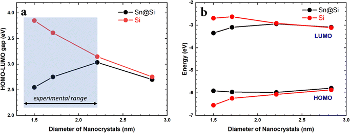 | ||
| Fig. 2 (a) HOMO–LUMO gap vs. NC diameter for pure Si-NCs (black) and Sn@Si-NCs (red). (b) HOMO and LUMO energies vs. NCs diameter for pure Si-NCs (red) and Sn@Si-NCs (black). | ||
A closer look at the trends of the HOMO and LUMO energies (Fig. 2b) shows that for pure Si NCs, the energy of the HOMO decreases monotonically and the energy of the LUMO increases monotonically with decreasing particle diameter, following the usual quantum confinement behaviour. For Sn@Si NCs in the diameter range 1.50–2.21 nm, we observe the opposite as the HOMO energy increases and the LUMO energy decreases with decreasing diameter, giving rise to the observed narrowing of the HOMO–LUMO gap for smaller NCs. For d = 2.21 nm the HOMO and LUMO energies of Sn@Si NCs are close to that for pure Si-NCs, and further increasing d increases the HOMO energy and decreases the LUMO energy, following the trend of pure Si NCs. The HOMO and LUMO of the smaller Sn@Si NCs are characterized by a state mainly involving Sn atoms and Si atoms in the vicinity of the incorporated Sn cluster. With increasing NC size, the states attributed to mainly Si atoms move up (down) for the HOMO (LUMO) until the Sn dominated HOMO (LUMO) drops (rises) below (above) the orbital energy of the Si dominated states, and the Sn@Si NCs eventually become indistinguishable with the pure Si NCs. Hence the orbital energies and thus the HOMO–LUMO gap converge towards the Si-NC values for large Sn@Si NCs.
2.2 Si–Sn NC synthesis and characterization
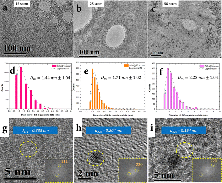
The synthesis of NCs was carried out by atmospheric pressure microplasma using a sacrificial wire electrode as the Sn precursor and gaseous silane as the silicon precursor in an argon/hydrogen background, see the ESI† for synthesis conditions and full experimental details. Three different and optimized synthesis conditions at three different argon–silane gas flows (15 sccm, 25 sccm and 50 sccm) allowed the formation of NCs with different size distributions (Fig. 3). Transmission electron microscopy (TEM) imaging confirms the formation of clearly separated NCs (Fig. 3a–c) where the size of the NCs was determined by the rate of argon–silane gas flow, with mean diameters of d = 1.4 nm for 15 sccm, d = 1.7 nm for 25 sccm and d = 2.2 nm for 50 sccm (Fig. 3d–f). Si–Sn NC separation could be due to negatively charged surfaces induced in the plasma which has also been reported for other nanoparticles.33 All three size distributions were found to be narrowly distributed (Fig. 3d–f). Fig. 2g–i shows representative high resolution TEM images of Si–Sn NCs from samples corresponding to the size distributions that produced mean diameters of around 1.4 nm, 1.7 nm and 2.2 nm. The lattice fringes can be seen clearly in Fig. 3g–i confirming the crystalline nature of Si–Sn NCs. The lattice spacing was found to be close to the lattice spacing of Si for (111) and (220) planes (0.313 nm and 0.192 nm, respectively). More specifically the lattice spacing of 0.333 nm, 0.204 nm and 0.194 nm were measured in the representative images of Fig. 3g–i and corresponding insets with fast Fourier transform (FFT) images. More measurements (see the ESI†) were produced from the analysis of several other NCs all revealing crystal spacing values in the ranges 0.316–0.333 nm and 0.193–0.198 nm, corresponding to the (111) and (220) planes of silicon. All these values reported a degree of expansion of the lattice spacing with respect to that of bulk silicon, possibly due to both the size of the nanocrystals as well as the inclusion of Sn.The surface of NCs possesses highly energetic atoms that must be passivated and it is normally being carried out with organic ligands.34,35 In the case of silane plasma, the dissociation of silane molecules leads to the growth of Si NCs with hydrogen passivated surfaces.33,36 In a similar way, our Si–Sn NCs shows hydrogen passivated surfaces with minor oxidation when it is exposed to air for short periods of time. The hydrogenated surfaces of Si–Sn NCs were confirmed from the Si–Hx absorption bands in the Fourier transform infrared (FTIR) as shown in Fig. 4.
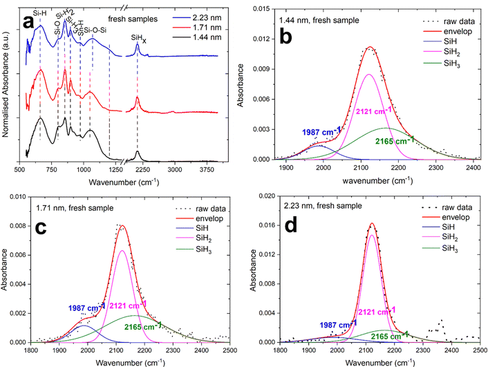
The characteristic absorbance peaks of surface passivated NCs from silane plasma are the Si–Hx (x = 1, 2, 3) bands. The Si–H bending vibrations have been reported to appear normally in the range 600–700 cm−1,37,38 in our results the Si–H peak is found at 667 cm−1 which is consistent with the literature. The SiH2 and SiH3 wag-bending modes is generally reported at 850 cm−1 and 900 cm−1.39 In our case, the SiH2 and SiH3 appears at 852 cm−1 and 898 cm−1 which is very similar to the value reported in the literature.39 The Sn–H band wagging mode is reported at 968 cm−1 and we also observe a very small absorption at 970 cm−1.40 The most distinguishing features of surface passivation in Si NCs is also the Si–Hx absorption bands appearing from 2000 cm−1 to 2200 cm−1.41 The OySi–Hx peak normally ranges from 2200 cm−1 to 2250 cm−1.38
The deconvolution of Si–Hx peaks are performed to understand the surface passivation and to investigate the back-bond oxidation, if any, in Si–Sn NCs. Fig. 4b–d represents the deconvolution of the Si–Hx absorption in the three peaks at 1987 cm−1, 2121 cm−1 and 2165 cm−1 which can be ascribed to Si–H, Si–H2 and Si–H3 respectively (generally expected at 2090 cm−1, 2110 cm−1 and 2130 cm−1).38 The Si–H peak in our Si–Sn NCs is shifted to a lower wavenumber and appears at 1987 cm−1 which could support the incorporation of Sn in the Si lattice; a similar shift has been also observed for the case of boron and phosphorous incorporation in Si.42 Furthermore, no OSi–H peak is found in the range of 2200–2250 cm−1 which suggests no back-bond oxidation. Further information on oxidation of Si is represented by the presence of Si–O–Si. The Si–O–Si stretching, bending and wagging bands are generally very sensitive and are normally observed around 1090 cm−1 and 800 cm−1 respectively.43 Furthermore, the Si–O–Si have also been reported to appear from 1000 cm−1 to 1100 cm−1 depending on the extent of oxidation and on the stoichiometric ratio of oxides.38 In addition to that, a shoulder peak at around 1200 cm−1 can be assigned to porosity in the oxides instead of Si–O–Si vibration modes in the material.43 In our case, Si–O–Si stretching and bending appears to be at around 1050 cm−1 and 800 cm−1 respectively; the low intensity indicates very low oxidation as this would be otherwise a prominent peak due to its high sensitivity. The wavenumbers also suggests that oxidation is partial and non-stoichiometric in nature. It is interesting to note here that the Si–O–Si peak shifts to around 1070 cm−1 and broadens for the 2.2 nm Si–Sn NCs compared to the 1.4 nm and 1.7 nm Si–Sn NCs. Furthermore, a weak shoulder peak is found in the FTIR spectra of the 2.2 nm Si–Sn NCs which indicates the presence of non-stoichiometric oxides.43 Finally, no oxidation for tin and no Sn–O bonds were observed, which generally produce absorption in the range 550–600 cm−1.44
A detailed analysis of Si–Sn NCs was also carried out using XPS (Fig. 5). The Si 2p and Sn 4d high resolution XPS spectra were used to corroborate the composition and to investigate any possible interactions between Si and Sn. The Si 2p includes the contribution of Si–Si bonding generally found at 99.3–99.7 eV.45,46 H-passivated Si has been reported to exhibit a peak about 0.5 eV higher than the elemental Si–Si peak, while extensively oxidized bonds (Si4+) would result in corresponding features at or above 104 eV.45 Finally, peaks between 101 eV and 103.5 eV are generally attributed to sub-oxides (Si1+, Si2+ and Si3+).45 Unfortunately, there has been no report about the exact position of the Sn–Si bond in the literature. Griffith et al., however, have studied the effect of adsorption of Sn atoms on the restructuring of the Si structure at the surface and found a significant shift of around 0.5 eV in the binding energies with respect to the Si–Si peak despite Si and Sn having similar electronegativity.47 In our case, the Si–Si peak is located around 99.3 eV for all the three samples as shown in Fig. 5a–c which is as expected. The second peak in the Si 2p spectra appears at around 100 eV for the three samples which can be assigned to Si–H according to the literature.45 However, this peak can also be due to Si–Sn bonds considering the possibility of charge transfer from the Sn atoms to the Si atoms. The sub-oxide peak is found at 102.4 eV (Fig. 5a, 1.44 nm), 101.9 eV (Fig. 5b, 1.71 nm) and 100.7 eV (Fig. 5c, 2.23 nm) which indicate different degrees of partial oxidation for the different NCs, i.e. less oxidation for larger NCs as it would be expected due to the trend of the volume to surface ratio.45
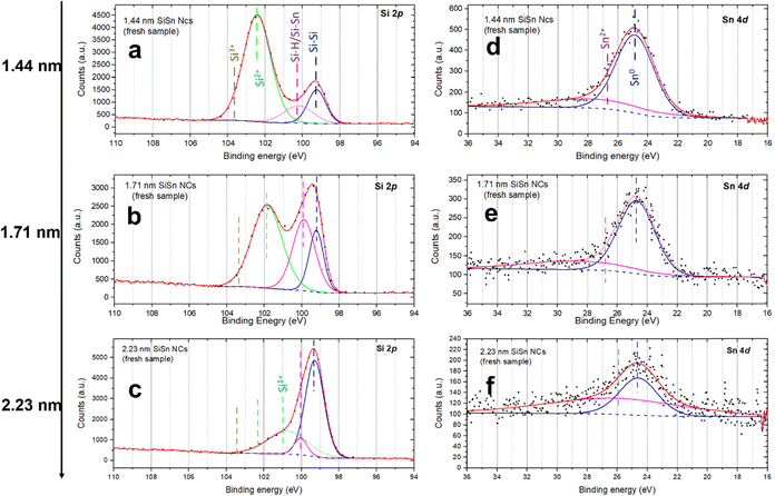 | ||
| Fig. 5 (a)–(c) The Si 2p spectra of 1.44 nm, 1.71 nm and 2.23 nm alloyed silicon–tin (Si–Sn) nanocrystals (NCs) respectively; (d)–(f) Sn 4d spectra of the corresponding Si–Sn NCs. | ||
In Fig. 5d–f, the Sn 4d is a doublet peak and hence includes Sn 4d5/2 and Sn 4d3/2 at 26.2 eV and 27.3 eV respectively.48,49 The peak associated with metallic tin (Sn0) lies at 25 eV.49 The Sn–Si bonding peak position is reported to be around 24.9 eV, which is too close to carry out a separate deconvolution.50 In Fig. 5d–f, the first peak is located at around 24.86 eV, 24.75 eV and 24.60 eV for 1.44 nm, 1.71 nm and 2.23 nm Si–Sn NCs respectively. These values show minor variations compared to the literature and located below 25 eV and therefore can be assigned to Sn–Sn or Si–Sn bonds. The deconvolution has also revealed the presence of a very weak peak at ∼26.3 eV in the Sn 4d spectra shown in Fig. 5d–f which can be assigned to Sn2+ (26.2 eV).49 However, this peak is indeed very weak which confirms almost no oxidation. Therefore, the analysis of the Sn 4d peak also supports the presence of Sn and the existence of Si–Sn bonds, suggesting successful incorporation of Sn in the Si lattice with minor oxidation at the Si surface sites.
The average atomic concentration of Sn in Si–Sn NCs, as estimated from XPS, were found to be around 3.7%, 1.9% and 1.2% in samples with NCs of mean diameters 1.4 nm, 1.7 nm and 2.2 nm, respectively (see the ESI†). These concentrations correspond to about 2 to 4 atoms per NC (Section SI-D in the ESI†). It is interesting to note that the concentration of Sn increases with decreasing the size of Si–Sn NCs which is achieved through decreasing the flow of silane/argon gas. We acknowledge that atomic concentrations determined from XPS measurements are not error-free. Our results here confirm the presence of a very low concentration of Sn and that even in consideration of large measurement errors, the NCs appear to include a few atoms (<10 atoms) and do not exhibit significant changes due to different synthesis conditions.
Overall, our materials characterization shows that our synthesis method can reproduce quite closely the NCs that we have studied theoretically, with a size distribution spanning the same diameter range used in the calculations (Fig. 2a). The concentration of Sn atoms is also consistent with the parameters used in the theoretical calculations. In both theoretical and experimental cases, the number of Sn atoms is constant irrespective of the NC size with one Sn cluster of 4 atoms (theory) and about 2–4 atoms (experiments) per NC. The experimental results also suggests that Sn atoms are not present at under-coordinated surfaces sites which is consistent with the predictions obtained from the computational modelling of the NCs. Oxidation is almost unavoidable experimentally; however our results confirm that surfaces are H-terminated for the most part at Si-sites (as per our calculations) with only minor oxidation. All our results have been produced minimizing exposure of the samples to air to limit the impact of oxidation. In order to assess the rate of surface changes and determine the viability of samples we have carried out an in-depth analysis of the Si–Sn NCs oxidation stages (see the ESI†), which indicated that oxidation could be limited if analysis were carried out within about a day from synthesis.
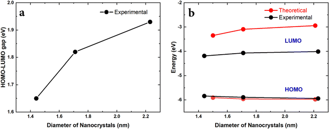
Finally, the HOMO–LUMO gap (Egap) was experimentally measured by surface photovoltage spectroscopy (SPS) and the HOMO energy (EH) was measured by air photoemission spectroscopy (APS). The LUMO energy (EL) could then be calculated EL = Egap + EH. We additionally determined the HOMO–LUMO gap using Tauc plots, which are very close to the direct measurement using SPS (see the ESI†). The results are summarized in Fig. 6.
2.3 Discussion
The experimental results relate to the NC size range as shown in Fig. 2a. This is the range where the theoretical results have shown an anomalous behaviour due to the presence of Sn-clusters, i.e. decreasing energy gap with decreasing diameter. Similarly, the experimental results show that decreasing the size of the NCs leads to a smaller HOMO–LUMO gap (Fig. 6a). Moreover, the corresponding trend of the HOMO and LUMO energies is consistent with the theoretical predictions (Fig. 6b). The absolute values of the HOMO energy from calculations and from experimental measurements are also in remarkable agreement. While the trend of the LUMO energy is also accurately reproduced in calculations, the theoretical absolute LUMO energy values are higher than those observed experimentally and hence calculations overestimate the HOMO–LUMO gap as compared to the measurements. This can be likely attributed to the fact that the SCAN0 functional used in the DFT calculations behaves relatively well for HOMO energies51 but tends to have larger errors for unoccupied orbitals. Additionally, in order to focus on the impact of cluster-doping, we neglected possible surface oxidation in the modelling of the Sn@Si NCs, which is, to some degree, always present in experiments. Oxidation generally results in reduced LUMO energies due to charge transfer.52 However, the measured trends are clearly consistent with our theoretical predictions and strongly supports the opportunities offered by cluster-doping vs. doping or alloying.We should note that we have carried out extensive simulations to verify if bandgap narrowing and HOMO/LUMO trends could be reproduced under different conditions. Doping with randomly distributed Sn atoms was ineffective to predict the experimental results. Similarly, the location of the Sn-cluster within the NCs was also important whereby only Sn-clusters that were located close to the surface were able to impact the electronic structure in the same way it was observed experimentally.
We can emphasize that the incorporation of the clusters in the nanocrystals is substantially different from other approaches, which use clusters to decorate materials or surfaces.53–55 The covalent bonding nature that is characteristic of ‘cluster-doping’ directly impact the electronic structure and fundamental properties of the nanocrystals, while cluster-decorated surfaces lack these intimate bonds and are unable to modify the fundamental electronic configuration of the host material.
The constant number of Sn atoms, irrespective of the NC size, also supports the mechanism of cluster-doping. This has also implications to understand the formation mechanisms of the cluster-doped NCs in the microplasma (Fig. 7). These results suggest that the interactions of the microplasma with the sacrificial Sn electrode produces Sn clusters or Sn atoms that subsequently cluster together in the plasma. Their growth into fully developed Sn nanoparticles30 is prevented by the plasma silane chemistry which leads to the simultaneous growth of Si NCs. It is unclear at what stage the Sn-cluster and growing Si NCs interact with each other; however, the asymmetric location of the Sn-clusters suggests that these do not act as nucleation sites for a silicon surface growth process as silicon nanocrystal growth does not require a catalyst or any seeding mechanism. Rather, the Sn-clusters attach to partially grown Si NCs. The Sn-clusters may remain close to the surface both because energetically favourable and because silicon growth stops, as the nanocrystals exit the plasma and growth is quenched.
The impact of this type of doping in Si NCs can be seen from the trends observed in the HOMO–LUMO and in the bandgap compared to undoped Si NCs as shown in Fig. 6b and also discussed earlier in the paper. The undoped Si NCs followed conventional quantum confinement behaviour whereas cluster doping resulted in a non-monotonic behaviour.
3. Conclusions
We have theoretically shown that ‘cluster-doping’ can provide an effective methodology to manipulate the electronic structure of NCs with substantial benefits for applications. Specifically, the trend of bandgap widening due to quantum confinement can be reversed. We have also demonstrated that NCs with the behaviour theoretically predicted from cluster-doping can be reproduced via atmospheric pressure microplasma synthesis. The NC size was controlled varying the flow of the silicon precursor while density of cluster-doping appeared to be unaffected within this range of synthesis conditions, i.e. one cluster per NC irrespective of the NC size. The formation mechanism of Si–Sn NCs involves the fragmentation of silane molecules in the plasma similar to the synthesis of Si NCs from silane. However, the likely presence of Sn clusters in the gas-phase enables their incorporation in the growing Si NCs. This work on the Si–Sn system suggests application opportunities for Sn@Sn NCs and encourage the investigation of cluster-doping with other NC compositions.Data availability
This paper is accompanied by representative samples of experimental data and the relevant numerical tabulated raw data is available from the University of Strathclyde's Research Portal at https://doi.org/10.15129/9de8afd7-e896-4357-a9b3-3e3f8733e4a1. Detailed procedures explaining how these representative samples were selected, and how these experiments can be repeated, are provided in the corresponding sections of this paper. Additional results and raw data underlying this work are available in the ESI† and at https://doi.org/10.15129/9de8afd7-e896-4357-a9b3-3e3f8733e4a1. Any other relevant data that may be missing can be provided upon request to the corresponding author.Conflicts of interest
There are no conflicts to declare.Acknowledgements
M. B. and V. S. acknowledge the support by Kakenhi 20H02579 by the Japanese Promotion of Sciences (JSPS). This work was supported by EPSRC (award no. EP/M024938/1, EP/V055232/1, and EP/R008841/1) and by DM Invitation and Bridge JSPS Fellowships.References
- R. Ferrando, J. Jellinek and R. L. Johnston, Chem. Rev., 2008, 108, 845 CrossRef CAS PubMed.
- G. Katsaros, P. Spathis, M. Stoffel, F. Fournel, M. Mongillo, V. Bouchiat, F. Lefloch, A. Rastelli, O. G. Schmidt and S. De Franceschi, Nat. Nanotechnol., 2010, 5, 458 CrossRef CAS PubMed.
- Y. Liang, Y. Li, H. Wang, J. Zhou, J. Wang, T. Regier and H. Dai, Nat. Mater., 2011, 10, 780 CrossRef CAS PubMed.
- D. Timmerman, J. Valenta, K. Dohnalová, W. D. A. M. de Boer and T. Gregorkiewicz, Nat. Nanotechnol., 2011, 6, 710 CrossRef CAS PubMed.
- F. Pulizzi, Nat. Nanotechnol., 2015 DOI:10.1038/nnano.2015.270.
- J. V. Lauritsen, J. Kibsgaard, S. Helveg, H. Topsøe, B. S. Clausen, E. Lægsgaard and F. Besenbacher, Nat. Nanotechnol., 2007, 2, 53 CrossRef CAS PubMed.
- R. Xu, P. Zhang, Q. Shen, Y. Zhou, Z. Wang, Y. Xu, L. Meng, D. Dang and B. Zhong Tang, Coord. Chem. Rev., 2023, 477, 214944 CrossRef CAS.
- P. Xiao, Z. Zhang, J. Ge, Y. Deng, X. Chen, J.-R. Zhang, Z. Deng, Y. Kambe, D. V. Talapin and Y. Wang, Nat. Commun., 2023, 14, 49 CrossRef CAS PubMed.
- E. Bossavit, T. H. Dang, P. He, M. Cavallo, A. Khalili, C. Dabard, H. Zhang, D. Gacemi, M. G. Silly, C. Abadie, B. Gallas, D. Pierucci, Y. Todorov, C. Sirtori, B. T. Diroll, A. Degiron, E. Lhuillier and A. Vasanelli, Adv. Opt. Mater., 2023, 11, 2300863, DOI:10.1002/adom.202300863.
- X. Wang, J. Zhuang, Q. Peng and Y. Li, Nature, 2005, 437, 121 CrossRef CAS PubMed.
- Q. An, W. Xiong, F. Hu, Y. Yu, P. Lv, S. Hu, X. Gan, X. He, J. Zhao and S. Yuan, Nat. Mater., 2024, 23, 347–355, DOI:10.1038/s41563-023-01590-5.
- D. J. Norris, A. L. Efros and S. C. Erwin, Science, 2008, 319, 1776 CrossRef CAS PubMed.
- F. P. García de Arquer, D. V. Talapin, V. I. Klimov, Y. Arakawa, M. Bayer and E. H. Sargent, Science, 2021, 373, 640, DOI:10.1126/science.aaz8541.
- A. B. Pun, A. J. Lyons and D. J. Norris, J. Chem. Phys., 2024, 160, 154711, DOI:10.1063/5.0201417.
- F. W. Eagle, S. Harvey, R. Beck, X. Li, D. R. Gamelin and B. M. Cossairt, ACS Nanoscience Au, 2023, 3, 451–461, DOI:10.1021/acsnanoscienceau.3c00029.
- X. D. Pi, R. Gresback, R. W. Liptak, S. A. Campbell and U. Kortshagen, Appl. Phys. Lett., 2008, 92, 123102, DOI:10.1063/1.2897291.
- G. Galli, Nature, 2005, 436, 32 CrossRef CAS PubMed.
- S. C. Erwin, L. Zu, M. I. Haftel, A. L. Efros, T. A. Kennedy and D. J. Norris, Nature, 2005, 436, 91 CrossRef CAS PubMed.
- C. R. Kagan and C. B. Murray, Nat. Nanotechnol., 2015, 10, 1013 CrossRef CAS PubMed.
- V. Švrček, D. Mariotti, R. A. Blackley, W. Z. Zhou, T. Nagai, K. Matsubara and M. Kondo, Nanoscale, 2013, 5, 6725 RSC.
- M. Lozac’h, V. Švrček, S. Askari, D. Mariotti, N. Ohashi, T. Koganezawa, T. Miyadera and K. Matsubara, Mater. Today Energy, 2018, 7, 87 CrossRef.
- M. Lozac’h, M. Bürkle, C. McDonald, T. Miyadera, T. Koganezawa, D. Mariotti and V. Švrček, Sci. Rep., 2023, 13, 7958 CrossRef PubMed.
- M. Bürkle, M. Lozac’h, C. McDonald, M. Macias-Montero, B. Alessi, D. Mariotti and V. Švrček, Adv. Funct. Mater., 2020, 30, 1907210, DOI:10.1002/adfm.201907210.
- J. Kouvetakis and A. V. G. Chizmeshya, J. Mater. Chem., 2007, 17, 1649 RSC.
- A. M. Hussain, N. Singh, H. Fahad, K. Rader, U. Schwingenschlögl and M. Hussain, J. Appl. Phys., 2014, 116, 224506, DOI:10.1063/1.4904056.
- S. Maiti, M. van der Laan, D. Poonia, P. Schall, S. Kinge and L. D. A. Siebbeles, Chem. Phys. Rev., 2020, 1, 011302, DOI:10.1063/5.0025748.
- M. Ferhat and A. Zaoui, Infrared Phys. Technol., 2001, 42, 81 CrossRef CAS.
- A. Tonkikh, A. Klavsyuk, N. Zakharov, A. Saletsky and P. Werner, Nano Res., 2015, 8, 3905 CrossRef CAS.
- X. Jin, S. Chen and T. Li, Phys. Rev. Mater., 2021, 5, 104606 CrossRef CAS.
- A. U. Haq, S. Askari, A. Mclister, S. Rawlinson, J. Davis, S. Chakrabarti, V. Svrcek, P. Maguire, P. Papakonstantinou and D. Mariotti, Nat. Commun., 2019, 10, 817, DOI:10.1038/s41467-019-08661-9.
- C. Chen and S. P. Ong, Nat. Comput. Sci., 2022, 2, 718 CrossRef PubMed.
- L. Brus, J. Phys. Chem., 1986, 90, 2555 CrossRef CAS.
- U. Kortshagen, J. Phys. D: Appl. Phys., 2009, 42, 113001 CrossRef.
- K. Kůsová, O. Cibulka, K. Dohnalová, I. Pelant, J. Valenta, A. Fŭcíková, K. Žídek, J. Lang, J. Englich, P. Matějka, P. Štěpánek and S. Bakardjieva, ACS Nano, 2010, 4, 4495 CrossRef PubMed.
- S. Prabakar, K. Fujioka, T. H. Lim, K. Yamamoto, P. T. Northcote and R. D. Tilley, J. Am. Chem. Soc., 2010, 132, 248 CrossRef PubMed.
- G. K. P. Dathar, Nano Lett., 2005, 5, 537 CrossRef PubMed.
- R. B. Wehrspohn, S. Lin, A. J. Flewitt, W. I. Milne and M. J. Powell, J. Appl. Phys., 2005, 98, 054505 CrossRef.
- D. Mariotti, V. Švrček, J. W. J. Hamilton, M. Schmidt and M. Kondo, Adv. Funct. Mater., 2012, 22, 954 CrossRef CAS.
- R. W. Liptak, B. Devetter, J. H. Thomas III, U. Kortshagen and S. A. Campbell, Nanotechnology, 2009, 20, 035603 CrossRef CAS PubMed.
- M. Stutzmann and J. Chevallier, Hydrogen in Semiconductors, Elsevier Science, 2012 Search PubMed.
- S. L. Weeks, B. MacCo, M. C. M. Van De Sanden and S. Agarwal, Langmuir, 2012, 28, 17295 CrossRef CAS PubMed.
- W. J. Sah and S. C. Lee, Doping-Induced Structural Change in Amorphous Silicon (Carbon) Hydrogen Alloy, in Amorphous and Crystalline Silicon Carbide II, ed. M. M. Rahman, C. Y. W. Yang and G. L. Harris, Springer Proceedings in Physics, Springer, Berlin, Heidelberg, 1989, vol. 43 DOI:10.1007/978-3-642-75048-9_16.
- J. Chou and S. Lee, J. Appl. Phys., 1995, 77, 1805 CrossRef CAS.
- A. Elci, O. Demirtas, I. M. Ozturk, A. Bek and E. Nalbant Esenturk, J. Mater. Sci., 2018, 53, 16345 CrossRef CAS.
- J. M. C. Thornton and R. H. Williams, Phys. Scr., 1990, 41, 1047 CrossRef CAS.
- C. Rocks, S. Mitra, M. Macias-Montero, P. Maguire, V. Svrcek, I. Levchenko, K. Ostrikov and D. Mariotti, ACS Appl. Mater. Interfaces, 2016, 8, 19012 CrossRef CAS PubMed.
- C. L. Griffiths, J. Vac. Sci. Technol., B: Microelectron. Nanom. Struct., 1993, 11, 1559 CrossRef CAS.
- F. A. Akgul, C. Gumus, A. O. Er, A. H. Farha, G. Akgul, Y. Ufuktepe and Z. Liu, J. Alloys Compd., 2013, 579, 50 CrossRef CAS.
- Z. Wang, H. a Al-Jawhari, P. K. Nayak, J. a Caraveo-Frescas, N. Wei, M. N. Hedhili and H. N. Alshareef, Sci. Rep., 2015, 5, 9617 CrossRef CAS PubMed.
- D. H. Rich, T. Miller, A. Samsavar, H. F. Lin and T. C. Chiang, Phys. Rev. B: Condens. Matter Mater. Phys., 1988, 37, 10221, DOI:10.1103/PhysRevB.37.10221.
- K. Hui and J.-D. Chai, J. Chem. Phys., 2016, 144, 044114, DOI:10.1063/1.4940734.
- M. Bürkle, M. Lozac’h, C. McDonald, D. Mariotti, K. Matsubara and V. Švrček, Adv. Funct. Mater., 2017, 27, 1701898, DOI:10.1002/adfm.201701898.
- W.-H. Lin, Y.-H. Chiu, P.-W. Shao and Y.-J. Hsu, ACS Appl. Mater. Interfaces, 2016, 8, 32754–32763, DOI:10.1021/acsami.6b08132.
- Y. Xiong, X. Liu, Y. Hu, D. Gu, M. Jiang, Z. Tie and Z. Jin, Nano Res., 2022, 15, 4965 CrossRef CAS.
- L. Guo, G. Zhang, R. Yang, D. Zhang, X. Zhang, H. Yu, X. Li and F. Dang, Nano Res., 2024, 17, 2678 CrossRef CAS.
Footnote |
| † Electronic supplementary information (ESI) available. See DOI: https://doi.org/10.1039/d4nh00235k |
| This journal is © The Royal Society of Chemistry 2024 |

