Surface modification of a biomass-derived self-supported carbon nano network as an emerging platform for advanced field emitter devices and supercapacitor applications†
Pallavi
Mutadak
 a,
Amol
Vedpathak
 b,
Sambhaji
Warule
 *cd,
Nilima
Chaudhari
 c,
Shrikrishna
Sartale
 a,
Mahendra
More
 *a and
Dattatray J.
Late
 *ef
*ef
aDepartment of Physics, Savitribai Phule Pune University, Pune-411007, India. E-mail: mam@physics.unipune.ac.in
bSymbiosis Center for Nanoscience and Nanotechnology, Symbiosis International University, Lavale, Pune-412 115, India
cDepartment of Physics, MES Nowrosjee Wadia College, S. P. Pune University, Pune-411001, India. E-mail: warulesam@gmail.com
dDepartment of Chemistry, Indian Institute of Science Education and Research, Pune-411008, India
eMaterials Science and Technology Group, Brane Enterprises Pvt Ltd, Hyderabad-500033, India. E-mail: datta099@gmail.com
fDepartment of Physics, Federal University of Lavras, Campus Universitário, PO Box 3037, Lavras, MG, Brazil
First published on 5th September 2024
Abstract
Herein, a self-supported carbon network is designed through the sole pyrolysis of Carica papaya seeds (biomass) without any activation agent, demonstrating their field emission and supercapacitor applications. The pyrolysis of seeds in an argon atmosphere leads to the formation of interconnected, rod-like structures. Furthermore, the hydrofluoric acid treatment not only removed impurities, but also resulted in the formation of CaF2 nanocrystals with the addition of F-doping. From the field emission studies, the turn-on field values defined at an emission current density of ∼10 μA cm−2 were found to be ∼2.16 and 1.21 V μm−1 for the as-prepared carbon and F-doped carbon, respectively. Notably, F-doped carbon exhibits a high emission current density of ∼9.49 mA cm−2 and has been drawn at an applied electric field of ∼2.29 V μm−1. Supercapacitor studies were carried out to demonstrate the multi-functionality of the prepared materials. The F-doped carbon electrode material exhibits the highest specific capacitance of 234 F g−1 at 0.5 A g−1. To demonstrate the actual supercapacitor application, the HFC//HFC symmetric coin cell supercapacitor device was assembled. The overall multifunctional applicability of the fabricated hybrid structures provides a futuristic approach to field emission and energy storage applications.
New conceptsWe have developed a single-step method to produce a self-supported carbon network, which sidesteps the traditional multi-stage process of making porous carbon materials. By directly pyrolyzing Carica papaya seeds at a lower temperature within an inert environment, we eliminate the need for additional activating agents. The obtained product has a high aspect ratio and hierarchical architecture, making it a perfect candidate for crafting the field emitters and supercapacitor electrodes. Our research also delves into the integration of heteroatoms through fluorine-doping and the concurrent formation of heterostructures like CaF2 nanocrystals within the carbon rod network, achieved by treating them with hydrofluoric acid. This innovative technique results in semi-ionic carbon–fluorine bonds, ideal fluorine doping levels, a decreased work function, and expanded interlayer distances, leading to superior field electron emission characteristics, increased specific capacity, and better cycling stability when compared to traditional amorphous carbon. These advanced hybrid structures and strategic doping amplify the multifunctionality of amorphous carbon, paving the way for the next generation of field emission based devices and energy storage solutions. |
1. Introduction
Carbon-based materials are increasingly capturing the attention of researchers across diverse fields, thanks to their exceptional versatility and multifunctional capabilities that surpass those of other materials. Notable among these materials are carbon nanotubes (CNTs), hollow carbon spheres, porous carbon, reduced graphene oxide, and graphene. These materials, especially CNTs and graphene, have demonstrated their effectiveness in a range of applications, including photovoltaics, vacuum electronics, field electron emission, and energy storage and conversion technologies.1–3 Moreover, activated microporous carbon, with its unique structural and electronic properties, holds the potential to introduce significant advantages when integrated with other materials. Controlled biomass pyrolysis is a prevalent synthesis method, chosen for its straightforward approach, scalability, and cost-effectiveness.4,5 Despite these advantages, the practical application of the resulting powdery carbon materials faces significant hurdles, including complex multistage synthesis, laborious electrode assembly for devices, and maintaining specific morphologies for targeted uses. Consequently, there is a strong interest in creating a streamlined, single-step process that can produce self-standing carbon structures without the need for a catalyst, which would be advantageous for a variety of applications.Field emitter arrays (FEAs) are at the forefront of research due to their potential to generate high-current density cathodes, which are crucial for display technologies and medical X-ray imaging.6,7 Carbon-based structures, such as 1D carbon nanotube (CNT) arrays and graphene, are being thoroughly investigated as candidates for cold cathode field emitters because of their impressive electrical and mechanical properties.8–10 Enhancements in field emission (FE) characteristics have been attributed to the innovative development of heterostructures and doping techniques.11,12 While methods like arc plasma and post-thermal treatment for creating heteroatom-doped carbons have garnered significant interest,13 the production of self-supported carbon structures through straightforward pyrolysis remains underexplored. Such structures offer the advantage of modulating the work functions through doping or heterostructure formation. Moreover, the design of self-assembled emitters with adequate spacing is critical for achieving high current density in field emitters.14 In parallel, carbon-based materials are recognized for their role in electric double-layer capacitive (EDLC) supercapacitors,15,16 valued for their extensive surface area, chemical and structural stability, and longevity. Despite these advantages, porous carbon materials often exhibit low specific capacitances, which limit their practical application. The introduction of heteroatoms into the carbon matrix has proven to be an effective strategy to enhance electrochemical performance by providing additional electron-donating or accepting sites, thereby increasing electrical conductivity, improving material-electrolyte interfacial wettability, introducing more structural defects and active sites, and facilitating ion species absorption.17,18 The creation of heterostructures through the low-temperature pyrolysis of biomass, which incorporates heteroatom doping, is a promising approach for applications requiring high-current density field emitters and energy storage.
This process has been effectively applied to Carica papaya seeds, resulting in self-supported, distinct carbon structures. The pyrolysis preserves the original form, dimensions, and self-organized patterns of the biomass. Additionally, treating the pyrolyzed seeds with hydrofluoric (HF) acid not only catalyzes with an increase of graphitic carbon but also enables successful fluorine doping. The resulting carbon structures, due to their graphitic nature and fluorine doping, offer improved conductivity and reduced screening effects, allowing for sufficient separation between emitters. This enhances the electric field, facilitating electron tunnelling at lower voltages and ensuring stable emission across a broader area. The objective of this research is to explore the potential of using carbon nano-networks derived from biomass as a versatile, cost-effective alternative to traditional cold cathodes and carbon-based electrochemical supercapacitors.
2. Experimental methods
Material synthesis
Field emission measurements
The field emission (FE) current versus applied voltage (I–V) and emission current versus time (I–t) characteristics were measured in a planar ‘diode’ configuration in an all-metal vacuum chamber evacuated to a base pressure of ∼1.0 × 10⁻⁸ mbar. In a typical ‘diode’ configuration, a phosphor-coated indium tin oxide glass plate (circular disc of diameter ∼50 mm) acts as the anode, whereas the as-synthesized seed of PC, HLC and HFC samples (pasted using ultra-high vacuum compatible conducting silver paste on a Cu rod of diameter 5 mm) served as the cathode. A typical photograph of a seed attached a Cu rod is shown in ESI,† Fig. S1d. At a constant cathode–anode separation of ∼2 mm, FE measurements were carried out. The emission current was acquired by varying the applied dc voltage between the cathode and anode with a step of 40 V (0–40 kV, Spellman, U.S.). Special care was taken to avoid any leakage current by ensuring proper grounding. The details of vacuum processing and FE measurements are described elsewhere.19Working electrode preparation for electrochemical studies
The working electrodes of the HLC and HFC samples were prepared using the Doctor's blade technique. First, HLC or HFC, activated carbon and polyvinylidene fluoride (PVDF) powders were mixed with a mass ratio of 8![[thin space (1/6-em)]](https://www.rsc.org/images/entities/char_2009.gif) :
:![[thin space (1/6-em)]](https://www.rsc.org/images/entities/char_2009.gif) 1
1![[thin space (1/6-em)]](https://www.rsc.org/images/entities/char_2009.gif) :
:![[thin space (1/6-em)]](https://www.rsc.org/images/entities/char_2009.gif) 1 using N-methylpyrrolidone (NMP) as a solvent. After this, the slurry was pasted on a conducting carbon paper substrate (1 cm × 1 cm area). Finally, the coated HLC and HFC electrodes were dried in a microwave oven at 150 °C for 12 h.
1 using N-methylpyrrolidone (NMP) as a solvent. After this, the slurry was pasted on a conducting carbon paper substrate (1 cm × 1 cm area). Finally, the coated HLC and HFC electrodes were dried in a microwave oven at 150 °C for 12 h.
Fabrication of the symmetric supercapacitor device
The HFC coin cell supercapacitor device was fabricated to demonstrate the practical supercapacitor application of the HFC sample. First, HFC electrodes were fabricated by the above-mentioned Doctor blade method on a carbon paper disk with a 12 mm diameter. The 1 M NaCl/PVA gel served as an aqueous electrolyte. The gel was prepared by mixing 1g of NaCl and 1 g of PVA into 10 mL DDW followed by constant stirring and heating at 80 °C. Finally, the HFC//HFC symmetric coin cell supercapacitor device was assembled by crimping these prepared HFC electrodes, a Whatman paper separator, metallic spacers and springs into CR 2032 coin cell cases. Before measurements, the fabricated SC devices were aged for 24 h.Electrochemical studies
All the electrochemical measurements were carried out on the IVIUM-Vertex single-channel potentiostat (Ivium Technologies BV, Netherlands). The saturated calomel electrode (SCE) and platinum wire were used as the reference and counter electrodes. All the electrochemical measurements were performed within the potential window of 0 to 0.6 V and with 1 M Na2SO4 aqueous electrolyte solution.3. Results and discussion
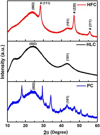
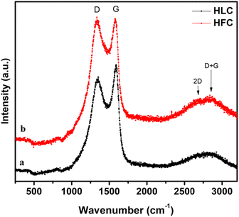
Fig. 1 depicts the XRD patterns of nano carbon samples of PC, HLC and HFC, synthesized at 800 °C for 1h. Two broad peaks around 22.27° and 42.12° represent the amorphous carbon formed predominantly present in all three samples, corresponding to the (002) and (101) planes, respectively. These diffraction peaks arise from the random orientation and stacking of aromatic sheets present. In the case of the PC powder sample, some additional sharp peaks are observed owing to impurities of the mineral compounds, namely MgO, Ca(CO)3, CaO, SiO2, etc. After being treated with HCL and HF, all present impurities were removed. Interestingly, relatively sharp peaks are observed in the HFC sample, along with the amorphous carbon nature. These peaks are indexed to (111), (220) and (311) planes, corresponding to the crystalline CaF2 present in the sample (JCPDS card no. 87-0971). The broadening indicates the formation of CaF2 nanosized crystals of size ∼10 nm, which is calculated from the Debye–Scherrer equation. No other impurity peaks are present in the case of HLC and HFC. Furthermore, the effect of variation in heat treatment temperature (800 °C and 900 °C) with different durations (1, 2 and 3 h) on the XRD patterns was also studied and presented in the ESI,† Fig. S2–S4.In support of XRD, Raman analysis will give an idea about the crystal structure and defects in the carbonaceous materials. Fig. 2 depicts the Raman spectra of HLC and HFC nano carbon samples. The carbonaceous material has two major Raman-active modes of vibration: a high-frequency E2g mode around ∼1580 cm−1 (G band), representing the bond-stretching of sp2 pairs in both rings and chains and a low-frequency A1g mode around ∼1339 cm−1 (D band) representing the breathing modes of atoms in rings and activated by the presence of some defects in the structure of the carbon materials. The ID/IG ratio gives an insight into the level of defects or disorder in the system, allowing us to understand the various factors contributing to the defects, like heterogeneous doping.20 The intensity of the D peak of the HFC sample is higher than that of the HLC sample. The HFC sample shows a larger ID/IG (1![[thin space (1/6-em)]](https://www.rsc.org/images/entities/char_2009.gif) :
:![[thin space (1/6-em)]](https://www.rsc.org/images/entities/char_2009.gif) 1) ratio value compared to the HLC sample (0.91), indicating the F-doping and CaF2 presence. A second-order peak called the 2D peak, at around ∼ 2700 cm−1, arises due to the presence of zone boundary phonons, which is a sensitive peak that broadens or even vanishes with various conditions. The HFC sample reveals a fairly resolved 2D peak proportional to the HLC sample, indicating the existence of 2D carbon sheets.
1) ratio value compared to the HLC sample (0.91), indicating the F-doping and CaF2 presence. A second-order peak called the 2D peak, at around ∼ 2700 cm−1, arises due to the presence of zone boundary phonons, which is a sensitive peak that broadens or even vanishes with various conditions. The HFC sample reveals a fairly resolved 2D peak proportional to the HLC sample, indicating the existence of 2D carbon sheets.
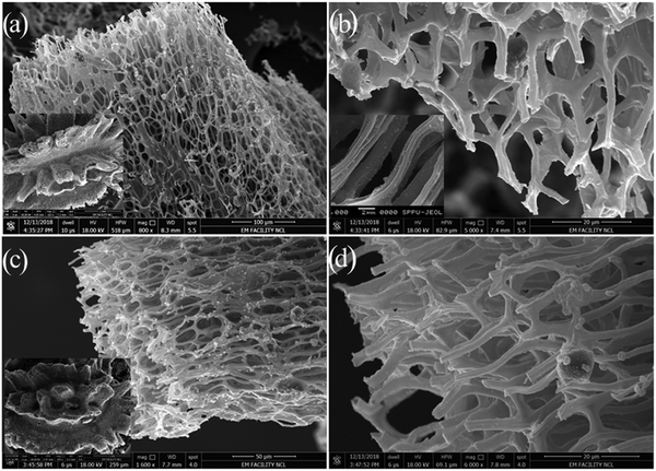
The surface morphology of the pyrolyzed seeds was examined using SEM. The pyrolysis of the seeds at 800 °C for 1 h in the Ar atmosphere results in the straightforward formation of geometrically defined and interconnected assembled rod-like structures (ESI,† Fig. S5), which indicates the shape preservation of biomass. Due to pyrolysis, some impurities were observed over the surface of the rods (ESI,† Fig. S5b–d), which are correlative and confirmed through the XRD pattern (Fig. 1) as well as EDS spectra (ESI,† Fig. S6) of the same sample. Furthermore, acid treatment is employed to remove such impurities. The HCl-treated (HLC) and HF-treated (HFC) samples demonstrated similar morphology having an interconnected rod as a carbon network, as shown in Fig. 3. The average diameter of the rods is observed to be ∼ 2 μm. In the case of the HFC sample, there is the presence of CaF2 nanoparticles (Fig. 3c), on the surface of carbon rods in comparison to the HLC sample.
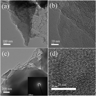
Furthermore, structural and morphological studies of HLC and HFC samples are performed using s transmission electron microscope (TEM). The TEM images of the HLC sample (Fig. 4) display an amorphous nature. Besides, these carbon regions [Fig. 4(a–c)] are attached to thin sheet carbon, which is amorphous in nature (the inset of Fig. 4c shows the conforming SAED pattern). The high-resolution TEM image (Fig. 4d) displays onion-like layers of fringes, which are commonly observed in amorphous carbon.
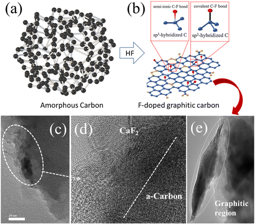
Fascinatingly, hydrofluoric acid-treated carbon illustrated CaF2 phase formation in the XRD pattern, which is further confirmed through TEM. The TEM images (Fig. 5a and c) depict CaF2 nanoparticles (∼10 nm) attached to nanorods (size ∼150 nm). The high-resolution TEM images (Fig. 5b and d) revealed the formation of the crystalline graphitic region. The interplanar spacing of ∼0.215 nm, corresponding to the (111) plane of CaF2, is observed. Additionally, the selected area electron diffraction (SAED) pattern (inset of Fig. 5b) indicated the crystalline nature. Moreover, from (Fig. 5d) in situ, growth of a crystalline CaF2 layer over an amorphous carbon (a-C) region is observed, which indicates surface modification. Fig. 5e depicts the partial formation of a graphitic sheet-like structure in the HFC sample, further confirmed through the HRTEM image (Fig. 5f) covering a d-spacing of ∼0.34 nm, corresponding to graphitic carbon. These results suggest that the HF treatment is essential for the formation of highly crystalline CaF2 nature inside the carbon structure.
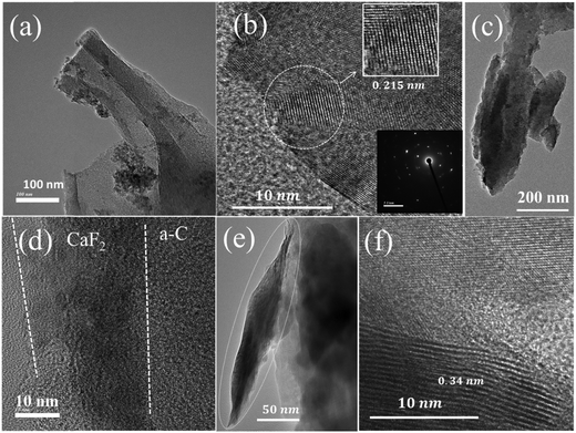 | ||
| Fig. 5 (a), (c) and (e) TEM and (b), (d) and (f) HRTEM images of the HFC sample with an inset displaying the corresponding SAED pattern. | ||
Fig. 6 depicts a low-magnified TEM micrograph and corresponding energy dispersive X-ray spectroscopy (EDX) elemental mapping images of the HFC sample. The elemental maps of C, Ca, and F exhibit a similar pattern to the TEM image. The TEM and EDX results are in good agreement with the XRD and XPS results. The distributed Ca and F evidently validate the formation of CaF2 nanoparticles with C on the composite sample. The combined mapping image of all elements and EDS spectra of the same sample with an inset show the elemental analysis (ESI,† Fig. S8).
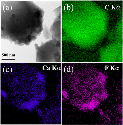 | ||
| Fig. 6 (a) TEM micrograph of the HFC sample and corresponding EDX elemental mappings images of (b) C Kα, (c) Ca Kα, and (d) F Kα. | ||
The elemental composition and chemical bonding state of the elements on the carbon surfaces were determined using XPS measurements. The XPS survey spectrum of the HFC sample is displayed in Fig. 7a, where C 1s, O 1s, Ca 2p and F 1s are present. The C 1s peak was found at ∼ 284.5 eV, the O 1s peak at ∼ 532.5 eV, the Ca 2p peak at 348.7 eV and the F 1s peak at ∼ 687 eV. The XPS survey spectrum of the PC and HLC samples is shown in the ESI,† Fig. S9. Fig. 7b presents the high-resolution XPS C 1s spectra with peak deconvolution of the HFC sample. The high-resolution XPS C 1s spectra of all three samples (ESI,† Fig. S9) display the most pronounced peak centered at 284.5 ± 0.1 eV, corresponding to the sp2 carbon bonding configuration. A long tail at higher binding energies is composed of several peaks assigned to sp3 carbon (285.4 ± 0.2 eV), C–O (286.4± 0.2 eV), C–F (288.2± 0.1 eV), and O–C–O (e.g., carbonyl and carboxylic: 289.7 ± 0.2 eV).13 Importantly, an additional weak intensity peak at 291.4 ± 0.2 eV appears for HFC, which authorizes the presence of the semi-ionic Csp2–F bonds.21 It is also worth noting that the sp2 peak intensity is slightly suppressed as fluorine doping occurs in the HFC sample. These results suggest that the incorporation of fluorine atoms causes structural deformation or lowers the degree of sp2 bonding of the carbon structure, which is consistent with the result from the Raman spectroscopy measurement and high-resolution TEM analysis.
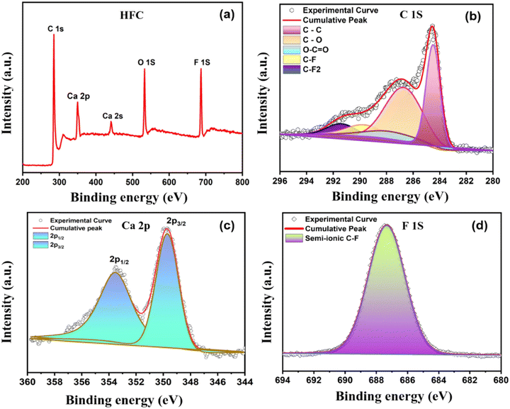 | ||
| Fig. 7 XPS analysis: (a) survey spectra, and (b) core level XPS spectra of C 1s, (c) Ca 2p and (d) F 1s of the HFC sample. | ||
In the Ca 2p core level binding energy spectrum, two prominent peaks at 349.2 and 352.6 eV are observed, which can be assigned as Ca 2p3/2 and Ca 2p1/2 peaks from the major CaF2 phase, respectively (Fig. 7c). Careful observation of the Ca 2p1/2 peak shows a slightly broadened peak with an FWHM of 2.37 eV, which indicates that the calcium is not present as a calcite or calcium carbonate phase but as calcium fluoride.22 A considerable shift towards higher binding energy is observed compared to the Ca 2p peaks of the original CaF2 phase, which can be attributed to the intimate chemical interaction with carbon structures.23 O 1s peaks in all samples are most likely the result of surface oxidation caused by air exposure of the samples. The detailed high-resolution XPS spectra of O1s for all three samples are shown in the ESI,† Fig. S10. Furthermore, the high-resolution deconvoluted XPS spectrum of F 1s for the HFC sample is given in Fig. 7d. The XPS F 1s of the HFC sample has a peak centred at 687.3 ± 0.2 eV, which can be assigned to a semi-ionic C–F bond. With fluorine doping, the π electrons contribute to the C–F bond and become more localized, resulting in C–F bond length and subsequently cherishing the semi-ionic characteristics. Fluorine atoms bonded to carbon atoms in semi-ionic type act as an electron acceptor, which subsequently facilitates charge transfer between fluorine and carbon, leading to higher conductivity as well as alteration of the electronic properties of the as-prepared carbon by boosting the graphitization.
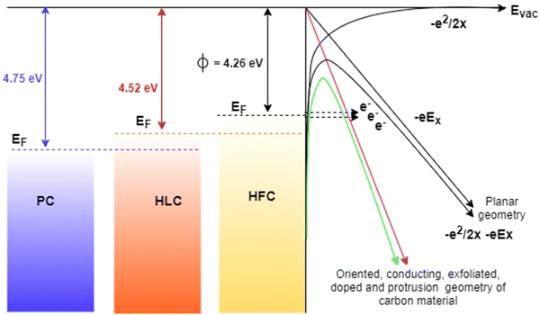
The work function (WF) of the synthesized samples was measured using UV photoelectron spectroscopy (UPS), as shown in Fig. 8. The WF can be obtained by subtracting the UPS spectrum width from the UV radiation energy (21.2 eV). The magnified UPS spectra around the secondary electron cutoff (Fig. 8d) indicate that the secondary electron cutoff shifted gradually to higher energy. This means that the WF of PC to HFC reduced gradually. Compared to PC (4.75 eV) and HLC (4.52 eV), the ϕ value of HFC decreases considerably (4.26 eV). This reduction in work function can evidence the formation of carbon–fluorine bonds.
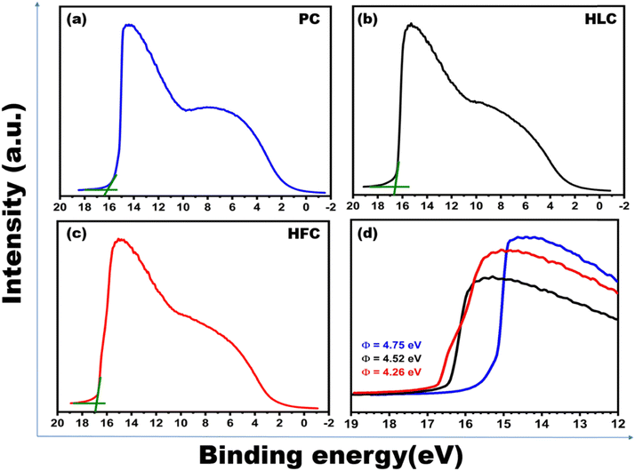 | ||
| Fig. 8 UPS spectra of (a) PC, (b) HLC and (c) HFC samples and (d) enlarged UPS spectra around the secondary cutoff energy. | ||
The BET surface area and the porosity of the prepared HLC and HFC were investigated. Fig. S11 and S12 (ESI†) show the nitrogen adsorption–desorption isotherm curves of the HLC and HFC samples. The BET surface area of the HLC and HFC samples is observed as 159.41 and 39.48 m2 g−1, respectively. Both samples have hierarchical self-assembled micro-sized rod-like structures; however, the rational design and construction of amorphous carbon with CaF2 and graphite nanocrystals, might play a crucial role here. Such design of heterostructures with amorphous/crystalline heterointerfaces is a straightforward and efficient method. The larger surface area is in general perceived to provide more active sites for reactions, and it was found in this work that crystallinity, which governs the charge transportation, has a more profound impact on influencing the supercapacitor application.
Field emission investigations
In the present study, the emission current density is defined as J = I/A (μA cm−2), where I is the emission current, and A is the area of the emitter. The applied electric field, also termed as an average electric field, is defined as, E = V/d, where V is the applied voltage, and d is the separation between the anode and cathode (1 mm). The values of turn-on and threshold fields are defined at emission current densities of 10 and 100 μA cm−2, respectively. From Fig. 9, the value of the turn-on field is observed to be 2.20, 2.12 and 1.22 V μm−1 for PC, HLC and HFC emitters, respectively. Whereas the value of the threshold field is observed to be 2.52, 2.32 and 1.41 V μm−1 for PC, HLC and HFC emitters, respectively. The turn-on and threshold field are found to be reproducible. With an increase in the applied field, the emission current density of all samples initially exhibits a gradual increase, and after the turn-on field, it increases exponentially, following the Fowler–Nordheim equation.24,25 The modified form of the Fowler–Nordheim equation is given as, | (1) |
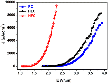 | ||
| Fig. 9 Field emission current density–applied electric field (J–E) plots of PC, HLC and HFC field electron emitters. | ||
As the applied electric field was increased further, the maximum emission current density of ∼6755, 8275 and 9477 μA cm−2 could be drawn from the PC, HLC and HFC emitters at an applied field of 3.92, 3.88 and 2.29 V μm−1, respectively. The emission current density drawn from the HFC emitter is approximately 1.40 and 1.14 times that of the PC and HLC emitter. The observed values of the turn-on field and threshold field of the HFC field emitter are much lower than those of the PC, HLC field electron emitters and earlier reported values for various carbon-based material emitters (Table 1).
| Sr. no. | Field emitters | Turn on field (V μm−1) | Threshold field (V μm−1) | Ref. |
|---|---|---|---|---|
| 1. | Q-Carbon | 2.4 (1 μA cm−2) | 2.65 (30 μA cm−2) | 26 |
| 2. | SWCNT | 2.05 V μm−1 (10 μA cm−2) | 2.5 V μm−1 (100 μA cm−2) | 27 |
| 3. | GO NCO | 2.9 V μm−1 | 28 | |
| 4. | Plasma treated GO | 2.5 V μm−1 (10 μA cm−2) | 2.78 V μm−1 (100 μA cm−2) | 29 |
| 5. | FRGO | 0.8 V μm−1 (10 μA cm−2) | — | 30 |
| 6. | PC | 2.20 (10 μA cm−2) | 2.52 (100 μA cm−2) | Present study |
| 7. | HLC | 2.12 (10 μA cm−2) | 2.32 (100 μA cm−2) | |
| 8. | HFC | 1.22 (10 μA cm−2) | 1.41 (100 μA cm−2) |
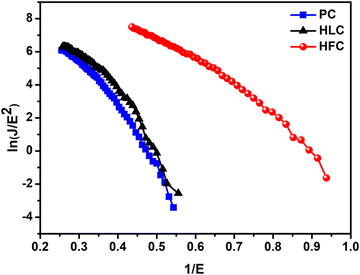
The observed J–E characteristic is further analyzed by plotting a graph of ln(J/E2) versus (1/E), known as an F–N plot. The F–N plot (Fig. 10) exhibits deviation from linear nature with a tendency towards saturation in the high field region. The deviation from linearity is attributed to the semiconducting nature of the emitter. Furthermore, for a planar emitter (composed of nanostructures deposited in thin film form on a suitable substrate), various factors, including variation in the aspect ratio of the nanostructures, field penetration and screening effect, band bending, etc. are responsible for the non-linear nature of the F–N plot.31 The relationship between the field enhancement factor (β) and the slope of the F–N plot (m) is expressed by the following equation,
 | (2) |
The value of work function (ϕ) calculated from UPS measurement is found to be ∼4.75, 4.52, and 4.26 eV for PC, HLC and HFC samples, respectively. Furthermore, the β values were estimated using the slopes (m) of ‘linearly fitting’ the F–N plot over the entire range of applied field, and using its slope, the value of β is estimated as 2281, 2344, and 3716 for PC, HLC and HFC, respectively. Such a large β value is representative of the high ‘aspect ratio’ of self-supported carbon-based materials.
Herein, the HFC sample has demonstrated remarkable effectiveness due to three main reasons: a semi-ionic C–F bond, desirable F doping degree, comparatively low work function, and enlarged interlayer distance yielded superior field electron emission properties. Such composites will be a benefit for enhancement in the field emission properties and the possible explanation is discussed below.
(i) Compared with HLC, HFC samples have a higher and broader asymmetric D band profile, resulting from a highly disordered amorphous carbon structure and hybridization structural change of C. Amorphous carbon with the presence of low graphitic order appears with increased ID in the HFC in comparison with the HLC sample. The ID/IG ratio reflects the degree of disorder in the HFC sample owing to the presence of C–F bonds. Recently, Jae Won Youn and co-workers have reported that the F-doped carbon layer is an effective surface modification method to enhance the intrinsic conductivity of active materials.32 This means that F doping leads to the lowering of the surface barrier, which in turn is expected to increase the carrier mobility and conductivity. It may also aid in the improvement of the mechanical properties of conductive composites. The pictorial form of amorphous carbon to F-doped graphitic carbon is shown in Scheme 1.
(ii) In the present HFC sample, in comparison with the HLC sample, instant formation of CaF2 nanocrystallites and graphitic content within the carbon matrix is observed. Due to the layered structure of graphite, its layers are possibly expanded and exfoliated with treatment to form high aspect ratio graphite with thickness in the nanoscale. The higher the aspect ratio of graphite, the easier it is to form a continuous network, even at a lower amount. The enhancement of interfacial interactions between graphite and the crystalline nature of CaF2 with carbon has been successfully done through the functionalization of carbon.
(iii) The field enhancement factor is related to the emitter geometry, crystal structure and spatial distribution of the emitting centers. Self-assembled morphology with sufficient spacing between each emitter plays a crucial role in the field enhancement. Also, these high-density protrusions (nanoscale) localize and enhance the electric field, thereby allowing electrons to tunnel through the tips at very low electric fields and produce stable emission in a large area.
(iv) At present, the surface states play an important role in influencing the carrier concentration, carrier mobility, conductance and barrier height, thereby governing its electron field emission properties. The nanometric protrusion features of graphite sheet and F-doping may increase the density of electronic states at the Fermi-level. This may lead to lowering the surface barrier, which in turn is expected to increase carrier mobility and conductivity. Also, the work function of the HFC (4.26 eV) sample, being smaller than that of the HLC (4.52 eV) sample, enables the transfer of electrons from rods to nanoparticles, giving rise to a higher carrier concentration.33 The energy band diagram of PC, HLC and HFC field emitters is shown in Scheme 2.
This is envisaged as potential emission sites coupled with a self-supported conductive substrate, facilitating excellent emission superior to the other nanostructure emitters.
The emission current stability is one of the important FE characteristics from an application point of view. In the present study, the emission current stability was studied at pre-set current value ∼10 μA over more than 3 h duration. A plot of the emission current (I) as a function of time (t) is depicted as the emission current stability behaviour of the HLC and HFC emitter (Fig. 11). It is observed that the emission current initially shows some excursions followed by stabilization at the pre-set values. Furthermore, the field emission current stability (I–t) plot of (a) HLC and (b) HFC emitters recorded at the base pressure of 1 × 10⁻⁸ mbar at pre-set current value ∼5 μA is shown in the ESI,† Fig. S13. The observations of excursions in emission current can be attributed to the ‘extinction’ and ‘regeneration’ of the emission sites. In addition, ‘spike’-like fluctuations are superimposed on the base current. Such fluctuations are attributed to various atomic scale processes such as adsorption, desorption, and/or migration of residual gaseous species on the emitter surface. Overall, the self-supported C emitter exhibits good emission current stability. A typical FE image recorded at the onset of emission current stability is depicted in the inset of Fig. 11. The image shows several bright lobes, which correspond to emission from the most protruding edges of the carbon material.
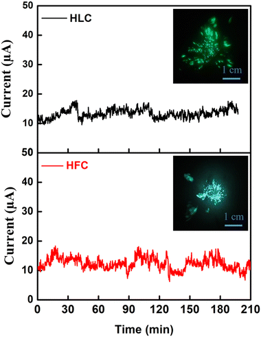 | ||
| Fig. 11 I–t Plot of (a) HLC and (b) HFC field electron emitters recorded at pre-set value ∼10 μA of emission current with the FE image shown in the inset. | ||
Electrochemical evaluation of HLC and HFC electrodes
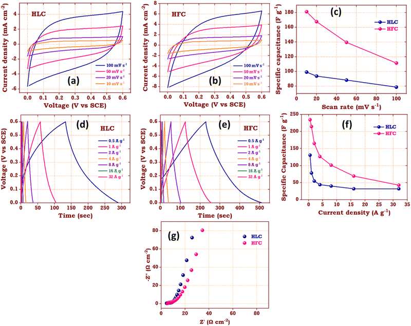
To evaluate the electrochemical behaviour of the HLC and HFC samples, various electrochemical characterizations were performed within a voltage range of 0–0.6 V in 1 M Na2SO4 electrolyte in a three-electrode system with SCE and platinum as a reference and counter electrode, respectively. Fig. 12a and b show CV curves for the HLC and HFC electrodes carried out at different scan rates ranging from 10–100 mV s−1. Both electrodes demonstrate nearly rectangular CV curves at a higher scan rate, indicating an electric double-layer capacitance behaviour of both electrode samples. However, the CV curve of the HFC electrode possesses more area under the curve than the HLC electrode, resulting in a higher charge storage capability of the HFC electrode.The specific capacitance (Csp) of the HLC and HFC electrodes from the CV measurements in a three-electrode system can be calculated from eqn (3)
 | (3) |
 gives the current for the charging and discharging process, m is the mass of the active material (g), v is the potential scan rate (mV s −1) and ΔV is the potential window used during CV measurement (V). The HFC sample exhibits the highest specific capacitance value of 181 F g−1. The graph of the calculated specific capacitance for different scan rates is plotted in Fig. 12c. This enhanced electrochemical behaviour may be due to the higher electric conductivity, high porosity and higher electro-active surface area of the HFC sample than the HLC sample. These obtained results align with the physicochemical and field emission characterization results. Additionally, GCD measurements were performed at current densities ranging from 0.5 to 32 A g−1 to investigate the charging–discharging characteristics of the HLC and HFC electrodes. Fig. 12d and e show the GCD curves of the HLC and HFC electrodes. The triangular GCD curves in both plots indicate the good capacitive behaviour of the HLC and HFC electrodes. The specific capacitance of the HLC and HFC electrodes was also determined from the GCD measurements from eqn (4)
 | (4) |
Electrochemical evaluation of the HFC//HFC coin cell supercapacitor device
The electrochemical measurements of HLC and HFC samples in a three electrode system implies that the HFC electrode possesses superior electrochemical properties than the HLC electrode. Therefore, to demonstrate the practical applications of the HFC sample, an HFC//HFC symmetric coin cell supercapacitor device was fabricated. To study the supercapacitor device characteristics of the HLC sample, we additionally fabricated an HLC//HLC symmetric supercapacitor coin cell device and their results are mentioned in ESI,† Fig. S14.Fig. 13 shows the electrochemical measurements of the fabricated HFC//HFC symmetric coin cell supercapacitor. Fig. 13a depicts the CV curves of the HFC//HFC supercapacitor for various scan rates in the potential range of 0–1.5 V. Here, the CV curves of the HFC//HFC supercapacitor device exhibit a rectangular shape for low scan rates and quasi-rectangular shape (observed in an electrode system) without any redox peak, indicating a typical double layer nature with a reversible non-faradaic process. Along with this, the wide operating potential window, a large area under the curve and the absence of a sharp increase or decrease in the current due to the water-splitting reaction imply the ideal supercapacitor behaviour of the fabricated device. By using eqn (3), the capacitance values from CV curves were calculated. The HFC//HFC supercapacitor device achieves the highest specific capacitance of 255.5 F g−1 at a scan rate of 10 mV s−1.
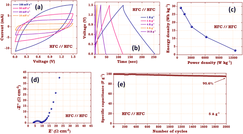 | ||
| Fig. 13 (a) CV, (b) GCD, (c) Ragone plot, (d) Nyquist plot and (e) cycling stability of the HFC//HFC coin cell supercapacitor device. | ||
Fig. 13b shows the GCD curves for the HFC//HFC supercapacitor device for various current densities ranging from 1 to 16 A g−1. All the GCD curves show symmetric triangular charging–discharging curves, which is the characteristic behaviour of the ideal supercapacitor device. In all the GCD curves, a very small ohmic drop was present, which may arise due to the small resistance owing to fast charge transfer and diffusion of electrolyte ions. Using eqn (4), the capacitance values were calculated. The HFC//HFC supercapacitor device demonstrates the highest specific capacitance of 93 F g−1 at a current density of 1 A g−1. With increasing current density, a gradual decrease in the specific capacitance was observed. This excellent value indicates that the HFC//HFC supercapacitor device has superior capacitive behavior and rate capability. By using these calculated specific capacitance values from GCD curves, the energy (E) and power density (P) values were calculated using the following equations.
 | (5) |
 | (6) |
![[thin space (1/6-em)]](https://www.rsc.org/images/entities/char_2009.gif) 500 W kg−1. EIS measurements (Fig. 13d) were carried out on the fabricated HFC//HFC supercapacitor device within the frequency range of 100 kHz to 10 mHz. The fabricated device shows a very low Rs value and small semi-circle corresponding to their low internal resistance and surface faradaic characteristics.35 A straight line slope in the lower frequency region corresponds to Warburg resistance demonstrating the capacitive nature of the HFC//HFC symmetric supercapacitor device. Moreover, the durability and life cycle performances of the HFC//HFC supercapacitor device were investigated using cycling stability measurements performed at a current density of 5 A g−1. Fig. 13e shows that the fabricated supercapacitor device exhibits ∼95.6% of its initial specific capacitance after 2000 GCD cycles, revealing the long cycle life of the fabricated supercapacitor device.
500 W kg−1. EIS measurements (Fig. 13d) were carried out on the fabricated HFC//HFC supercapacitor device within the frequency range of 100 kHz to 10 mHz. The fabricated device shows a very low Rs value and small semi-circle corresponding to their low internal resistance and surface faradaic characteristics.35 A straight line slope in the lower frequency region corresponds to Warburg resistance demonstrating the capacitive nature of the HFC//HFC symmetric supercapacitor device. Moreover, the durability and life cycle performances of the HFC//HFC supercapacitor device were investigated using cycling stability measurements performed at a current density of 5 A g−1. Fig. 13e shows that the fabricated supercapacitor device exhibits ∼95.6% of its initial specific capacitance after 2000 GCD cycles, revealing the long cycle life of the fabricated supercapacitor device.
It is notable that, by comparing the performance of the HFC//HFC supercapacitor device with the HLC//HLC supercapacitor device (ESI,† Fig. S14), it is clear that the HFC//HFC supercapacitor device displays superior electrochemical performance than the HLC//HLC supercapacitor device in terms of specific capacitance, energy and power densities and cycling stability.
4. Conclusions
A carbon network that is self-supported has been developed by the exclusive pyrolysis of PAPAYA seeds at 800 °C, eliminating the need for any activating substances. Our approach aims to improve the graphitization of carbon materials while also incorporating fluorine doping, which was achieved through hydrofluoric acid treatment. Remarkably, these composite structures show superior field emission characteristics when benchmarked against the initial preparations and other carbon derivatives. The electrochemical efficacy of these carbon electrode materials has been effectively validated within a tri-electrode configuration. Notably, the F-treated carbon electrode material exhibits 234 F g−1 of specific capacitance value at 0.5 A g−1 of current density. To demonstrate the actual supercapacitor application, the HFC//HFC symmetric coin cell supercapacitor device was assembled. This device can provide a wide working potential of 1.5 V with the highest energy density of 29 W h kg−1 and a power density of 12500 W kg−1. The superior performance of the field emission and supercapacitors can be attributed to the unique self-assembled rod-like structures. These structures are strategically spaced to prevent the screening effect. Additionally, the incorporation of heteroatoms, the crystalline form of graphite, and a reduced work function collectively enhance electrical conductivity, contributing to the impressive results observed.Author contributions
Dr PM— Experimental synthesis of carbon nano-network, Data curation and analysis of characterizations, experimental investigation on field emission and electrochemical studies, Writing—original draft. Dr AV—Experimental investigation electrochemical studies. Dr SW— Conceptualization, Formal analysis, Writing—original draft, Interpretation of measurements and Corresponding Author. Dr NC—Review and editing. Prof. SS: Review and editing. Prof. MM— Supervision, Corresponding Author, Approval of final draft. Dr DL— Supervision, Corresponding Author, Approval of final draft.Data availability
The data will be available from the authors on reasonable request.Conflicts of interest
There is no conflict of interest.Acknowledgements
SW expresses sincere gratitude for the financial support received from the SERB-TARE project (TAR/2020/000257). MM would like to acknowledge the financial support from the DST, Govt. of India under the Indo-French Centre for the Promotion of Advanced Research (IFCPAR/CEFIPRA) project 68TF-1 for carrying out Field Emission work.References
- J. Liu, R. Li and B. Yang, ACS Cent. Sci., 2020, 6, 2179–2195 CrossRef CAS PubMed
.
- M. M. Sabzehmeidani, S. Mahnaee, M. Ghaedi, H. Heidari and V. A. Roy, Mater. Adv., 2021, 2, 598–627 RSC
.
- B. Jaleh, M. Nasrollahzadeh, M. Eslamipanah, A. Nasri, E. Shabanlou, N. R. Manwar, R. Zboril, P. Fornasiero and M. B. Gawande, Carbon, 2022, 198, 301–352 CrossRef CAS
.
- J. Deng, M. Li and Y. Wang, Green Chem., 2016, 18, 4824–4854 RSC
.
- L. Sun, Y. Gong, D. Li and C. Pan, Green Chem., 2022, 24, 3864–3894 RSC
.
- S. Kumar, G. Duesberg, R. Pratap and S. Raghavan, Appl. Phys. Lett., 2014, 105, 103107 CrossRef
.
- S. Tsujino, P. Das Kanungo, M. Monshipouri, C. Lee and R. D. Miller, Nat. Commun., 2016, 7, 13976 CrossRef CAS PubMed
.
- A. Haque, S. Karmakar, R. K. Trivedi, B. Chakraborty and R. Droopad, ACS Omega, 2023, 8, 9307–9318 CrossRef CAS PubMed
.
- S. Riyajuddin, S. Kumar, K. Soni, S. P. Gaur, D. Badhwar and K. Ghosh, Nanotechnology, 2019, 30, 385702 CrossRef CAS PubMed
.
- S. Tang, Y. Zhang, P. Zhao, R. Zhan, J. Chen and S. Deng, Nanoscale, 2021, 13, 5234–5242 RSC
.
- S. S. Warule, N. S. Chaudhari, B. B. Kale, K. R. Patil, P. M. Koinkar, M. A. More and R.-I. Murakami, J. Mater. Chem., 2012, 22, 8887–8895 RSC
.
- S. R. Rondiya, C. D. Jadhav, P. G. Chavan and N. Y. Dzade, Sci. Rep., 2020, 10, 2358 CrossRef CAS PubMed
.
- G. Panomsuwan, N. Saito and T. Ishizaki, J. Mater. Chem. A, 2015, 3, 9972–9981 RSC
.
- P. R. Mutadak, S. S. Warule, P. S. Kolhe, P. K. Bankar and M. A. More, Surf. Interfaces, 2023, 41, 103251 CrossRef CAS
.
- D. Puthusseri, V. Aravindan, S. Madhavi and S. Ogale, Energy Environ. Sci., 2014, 7, 728–735 RSC
.
- Z. Zhai, L. Zhang, T. Du, B. Ren, Y. Xu, S. Wang, J. Miao and Z. Liu, Mater. Des., 2022, 221, 111017 CrossRef CAS
.
- T. Periyasamy, S. P. Asrafali and S.-C. Kim, Polymers, 2023, 15, 1564 CrossRef CAS PubMed
.
- Z. Lu, X. Liu, T. Wang, X. Huang, J. Dou, D. Wu, J. Yu, S. Wu and X. Chen, J. Colloid Interface Sci., 2023, 638, 709–718 CrossRef CAS PubMed
.
- P. K. Bankar, P. S. Kolhe, P. R. Mutadak, A. Kawade, K. M. Sonawane and M. A. More, Phys. E, 2021, 125, 114363 CrossRef CAS
.
- Y. Liu, Q. Li, X. Guo, X. Kong, J. Ke, M. Chi, Q. Li, Z. Geng and J. Zeng, Adv. Mater., 2020, 32, 1907690 CrossRef CAS PubMed
.
- X. Wang, Y. Dai, J. Gao, J. Huang, B. Li, C. Fan, J. Yang and X. Liu, ACS Appl. Mater. Interfaces, 2013, 5, 8294–8299 CrossRef CAS PubMed
.
- S. Budyanto, Y.-L. Kuo and J. Liu, Sep. Purif. Technol., 2015, 150, 325–331 CrossRef CAS
.
- C. d S. Bezerra and M. E. Valerio, Phys. B, 2016, 501, 106–112 CrossRef CAS
.
- R. G. Forbes, J. Appl. Phys., 2008, 104, 084303 CrossRef
.
- R. G. Forbes, Appl. Phys. Lett., 2006, 89, 113122 CrossRef
.
- A. Haque and J. Narayan, Diamond Relat. Mater., 2018, 86, 71–78 CrossRef CAS
.
- M. Song, Phys. B, 2021, 603, 412766 CrossRef CAS
.
- P. C. Maity and I. Lahiri, Appl. Surf. Sci., 2022, 591, 153186 CrossRef
.
- M. M. H. Raza, S. Khan, S. M. Aalam, M. Sadiq, M. Sarvar, M. Zulfequar, S. Husain and J. Ali, Carbon Trends, 2021, 5, 100127 CrossRef CAS
.
- K. Zhang, S. Wu, X. Yang, B. Wang, W. Wu, J. Qian, W. Ou-Yang, R. Zhao, Y. Song and Z. Sun, Mater. Res. Express, 2019, 6, 075608 CrossRef CAS
.
- R. H. Fowler and L. Nordheim, Proc. R. Soc. London, Ser. A, 1928, 119, 173–181 CAS
.
- J. W. Youn, G. H. Park, M. Kim, S. K. Kang, D. Jang and W. B. Kim, ACS Appl. Electron. Mater., 2023, 5, 4344–4353 CrossRef CAS
.
- N. Pakhira and R. Mahato, Physica B, 2023, 670, 415394 CrossRef CAS
.
- A. Vedpathak, T. Shinde, M. A. Desai, B. R. Thombare, R. Humane, S. A. Raut, R. Kalubarme, S. D. Sartale and S. Bhagwat, ACS Appl. Energy Mater., 2023, 6, 4693–4703 CrossRef CAS
.
- B.-A. Mei, O. Munteshari, J. Lau, B. Dunn and L. Pilon, J. Phys. Chem. C, 2018, 122, 194–206 CrossRef CAS
.
Footnote |
| † Electronic supplementary information (ESI) available. See DOI: https://doi.org/10.1039/d4nh00314d |
| This journal is © The Royal Society of Chemistry 2024 |

