
Instantaneous growth of single monolayers as the origin of spontaneous core–shell InxGa1−xN nanowires with bright red photoluminescence
Vladimir G.
Dubrovskii
*a,
George E.
Cirlin
abc,
Demid A.
Kirilenko
a,
Konstantin P.
Kotlyar
abc,
Ivan S.
Makhov
d,
Rodion R.
Reznik
 abc and
Vladislav O.
Gridchin
abc
abc and
Vladislav O.
Gridchin
abc
aFaculty of Physics, St. Petersburg State University, Universitetskaya Embankment 13B, 199034 St. Petersburg, Russia. E-mail: dubrovskii@mail.ioffe.ru
bAlferov University, Khlopina 8/3, 194021 St. Petersburg, Russia
cInstitute for Analytical Instrumentation RAS, Rizhsky 26, 190103 St. Petersburg, Russia
dHSE University, Kantemirovskaya 3/1 A, 194100 St. Petersburg, Russia
First published on 9th October 2024
Abstract
Increasing the InN content in the InxGa1−xN compound is paramount for optoelectronic applications. It has been demonstrated in homogeneous nanowires or deliberately grown nanowire heterostructures. Here, we present spontaneous core–shell InxGa1−xN nanowires grown by molecular beam epitaxy on Si substrates at 625 °C. These heterostructures have a high InN fraction in the cores around 0.4 and sharp interfaces, and exhibit bright photoluminescence at 650 nm. The surprising effect of material separation is attributed to the periodically changing environment for instantaneous growth of single monolayers on top of nanowires. Due to a smaller collection length of N adatoms, each monolayer nucleates under a balanced V/III ratio, but then continues under highly group III rich conditions. As a result, the miscibility gap is suppressed in the cores but remains in the shells. These results provide a simple method for obtaining high-quality InGaN heterostructures emitting in the extended wavelength range.
New conceptsObtaining high InN contents in InxGa1−xN is complicated by the miscibility gap, which closes only at 1250 °C. Fast growth kinetics in different nanostructures including nanowires helps to circumvent this issue. Our study goes beyond spatially homogeneous InGaN nanowires or deliberately grown InGaN/GaN heterostructures. We show that catalyst-free MBE growth of InGaN nanowires on Si substrates at 625 °C leads to the spontaneous formation of an In-rich core (with an InN fraction of 0.4) and an almost pure GaN shell. This effect is explained by the periodically changing growth conditions for instantaneous growth of single nanowire monolayers. The monolayer growth starts under a balanced V/III ratio for the diffusion fluxes in the core, leading to the kinetic suppression of the miscibility gap. When almost all N adatoms are removed from the surrounding surfaces, further growth occurs under highly group III rich conditions. This yields close-to-equilibrium composition of the shell, with negligible fraction of InN due to the miscibility gap. The role of instantaneous mononuclear growth in the nanowire composition and the very possibility of obtaining high-quality heterostructures in catalyst-free nanowires is revealed here for the first time, and can be translated to other material systems and growth techniques. |
1. Introduction
Ternary InGaN compounds1 and InGaN nanomaterials of different types including nanowires (NWs)2–8 are of tremendous interest for solid state lighting, renewable energy sources, and emitters of non-classical light. Due to a very efficient relaxation of elastic stress on strain-free sidewalls, III–V NWs can be grown on lattice-mismatched Si substrates without structural defects or with largely reduced dislocation density compared to epi-layers.9–11 This advantage was fully realized in catalyst-free GaN NWs and III-nitride ternary NWs.12–20 Fabrication of green and red light sources requires large fractions of InN in ternary InxGa1−xN. This is complicated due to the miscibility gap in the InGaN compound, which closes only at 1250 °C.21–23 It is well documented that nanomaterials offer much wider opportunities for compositional tuning compared to epi-layers.24 In particular, nearly the full compositional range of InxGa1−xN was achieved either in spatially homogeneous NWs or deliberately grown NW heterostructures, where the miscibility gap was suppressed on kinetic grounds.18–20,25–32In this work, we further develop the approach of ref. 20, 29 and 30 and show that high-quality core–shell InGaN NWs with a high InN fraction in the core (∼0.4) (corresponding to red emission around 650 nm) and an almost negligible InN fraction in the shell (∼0.04) form spontaneously in molecular beam epitaxy (MBE) on Si substrates at 625 °C. We speculate that spontaneous material separation in catalyst-free NWs is due to a transition from balanced to group III rich conditions for instantaneous growth of a single NW monolayer (ML). This effect should be general in NWs, and may be used for obtaining core–shell structures with sharp heterointerfaces for optoelectronic applications without any commutation of material fluxes.
2. Experimental procedures
InGaN NWs with spontaneously formed core–shell structures were grown on one-side polished p-type Si (111) substrates with a resistivity of 3.6 to 5 Ohm cm. Growth experiments were carried out in a Riber Compact 12 MBE system, equipped with an Addon RF-N 600 plasma source and Knudsen cells of Ga and In. To remove silicon oxide from the growth surface, the substrate was treated in a solution of hydrofluoric acid and deionized water (in a ratio of 1![[thin space (1/6-em)]](https://www.rsc.org/images/entities/char_2009.gif) :3) before growth. Then, the substrate was loaded into the MBE chamber and thermally annealed at 950 °C for 20 min. After that, the substrate temperature was decreased to 625 °C, as measured using an Optris CT Laser 3MH1 pyrometer. The nitrogen plasma was ignited at a source power of 450 W and a nitrogen flow of 1.4 × 10⁻⁵ torr. To initiate the growth of InGaN NWs, Ga and In shutters were simultaneously opened without preliminary formation of any seed layers. The beam equivalent pressures of the metal sources (In and Ga) were equal to each other and corresponded to 1 × 10⁻⁷ Torr, as measured with a Bayard Alpert gauge. The growth was carried out under a slightly N-rich environment, with a total V/III ratio of ∼1.1, according to our previous results.30 The total growth time was 21 hours.
:3) before growth. Then, the substrate was loaded into the MBE chamber and thermally annealed at 950 °C for 20 min. After that, the substrate temperature was decreased to 625 °C, as measured using an Optris CT Laser 3MH1 pyrometer. The nitrogen plasma was ignited at a source power of 450 W and a nitrogen flow of 1.4 × 10⁻⁵ torr. To initiate the growth of InGaN NWs, Ga and In shutters were simultaneously opened without preliminary formation of any seed layers. The beam equivalent pressures of the metal sources (In and Ga) were equal to each other and corresponded to 1 × 10⁻⁷ Torr, as measured with a Bayard Alpert gauge. The growth was carried out under a slightly N-rich environment, with a total V/III ratio of ∼1.1, according to our previous results.30 The total growth time was 21 hours.
Morphological properties of InGaN NWs were studied using a Carl Zeiss Supra 25 scanning electron microscope (SEM). The microstructure and chemical composition of the NWs were investigated by high-angle annular dark-field scanning transmission electron microscopy (HAADF STEM, Jeol JEM-2100F TEM) using the energy-dispersive X-ray (EDX) spectroscopy technique (XFlash 6TI30, Bruker). To measure the chemical composition in the cores and shells, the NWs were mechanically separated from the Si substrate and transferred to the TEM grid. This procedure allowed us to obtain different parts of the NWs both in the top-view and cross-sectional view geometry with respect to the TEM electron gun and detector. The EDX data were measured from NWs in the top-view geometry. This readily yields the actual In composition inside the core and shell of the NWs, without any adjustments for the core and shell thickness. To obtain the representative chemical compositions, we collected the EDX data from 15 NWs. The measurements were carried out from edge to edge of each NW in the point-by-point regime. Optical properties of the NWs were investigated using room-temperature photoluminescence (PL) spectroscopy. The PL was excited using a He–Cd laser (325 nm) with a spot diameter of about 1 μm. A silicon CCD matrix was used as a detector.
3. Results and discussion
Fig. 1(a) demonstrates the typical SEM image of an InGaN NW array. The average length, diameter, and surface density of these NWs are 2.8 μm, 100 nm, and 3 × 109 cm−2, respectively. Fig. 1(b) shows the typical STEM image and the corresponding EDX maps of Ga and In atoms at the NW top, evidencing the spontaneously formed core–shell structure. The STEM image demonstrates the sharp heterointerface between the core and the shell. The InN contents in the core and shell are 40 ± 3% and 4 ± 2%, respectively, according to the STEM EDX scan perpendicular to the NW axis (Fig. 1(c)). This scan represents the data collected from 15 individual NWs. The InN compositions in the core and shell regions are reproducible. The inner structure of the NW array is schematically shown in Fig. 1(d). In addition to the core–shell structure formed at a certain height, there is an intermediate InGaN/Si layer formed in the early stage of NW growth. It does not form a core–shell structure, as previously documented,29 but serves as a virtual substrate for the subsequent core–shell NWs.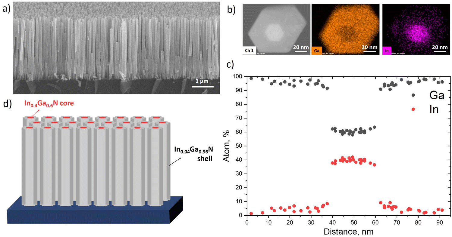 | ||
| Fig. 1 (a) SEM image of InGaN NWs. (b) STEM image of the NW top, with the corresponding Ga and In atomic maps obtained by EDX measurements. (c) STEM-EDX scan measured perpendicular to the NW tops. (d) Schematic structure of the whole sample. | ||
Fig. 2 shows the typical selected area diffraction (SAED) patterns, obtained by TEM measurements of individual NWs in the top-view and cross-sectional geometries. The measured SAED patterns from different NWs demonstrate their single crystalline structure in the wurtzite phase, with no observable extended defects such as dislocations or stacking faults.
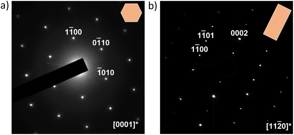 | ||
| Fig. 2 SAED patterns from InGaN NW in (a) top-view and (b) cross-sectional view geometry. | ||
Fig. 3(a) shows the typical PL spectra of the NW array, measured at different excitation power densities. To clarify the nature of the observed PL, the InN fraction in the NWs was deduced from the modified Vegard's law with a bowing parameter of 1.43 eV (ref. 20 and 29). The obtained results indicate that the two PL bands, observed in all spectra, originate from the InN-rich cores (the peak at ∼650 nm) with an InN fraction of ∼44%, and the InN-poor shells (the peak at ∼400 nm), with an InN fraction of ∼7%. The small deviations from the STEM EDX data can be explained by the Stock's shift and temperature dependence of the PL maxima. Fig. 3(b) shows the dependence of the integral PL intensity on the excitation power density, which was varied from 550 to 2 × 10⁵ W cm−2. The emission wavelengths from 550 to 750 nm correspond to the PL signals from the NW cores. The dependence is approximated by the power law
| I = CPγ, | (1) |
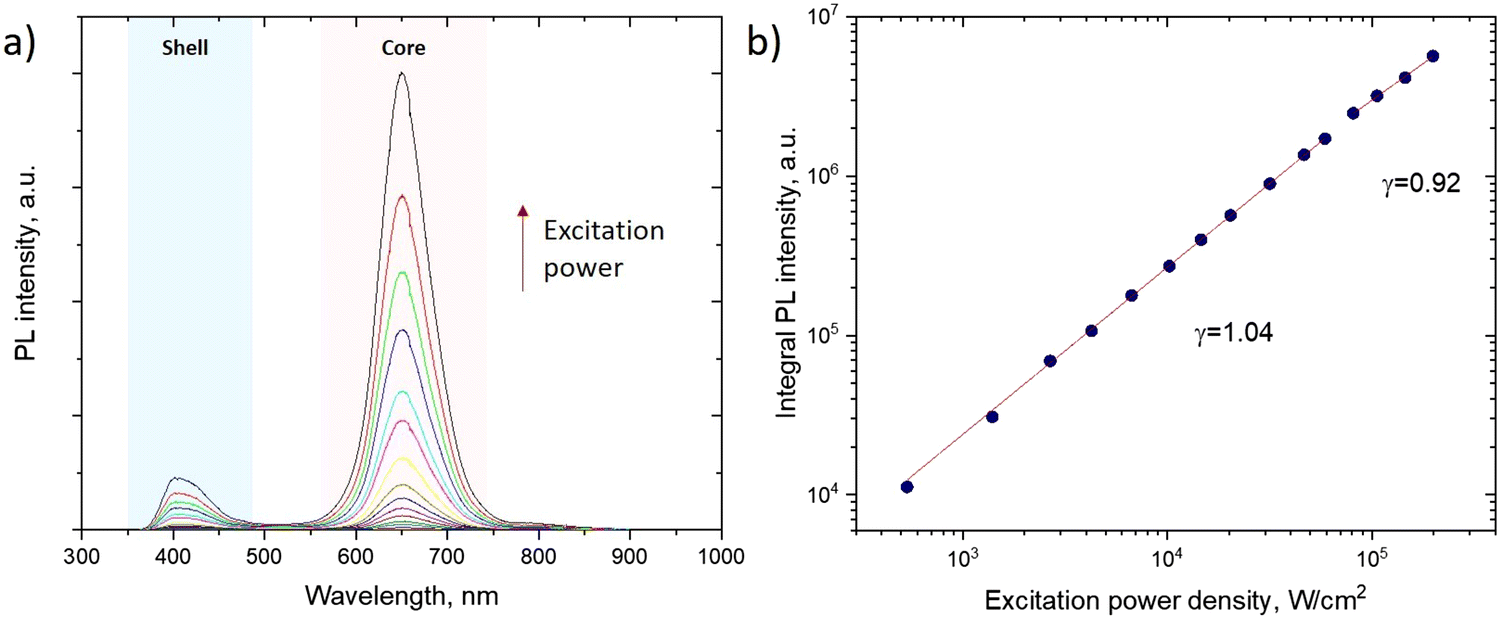 | ||
| Fig. 3 (a) PL spectra of InGaN NWs, measured at different excitation power densities. (b) Dependence of the integral PL intensity from the NW cores on the excitation power density (symbols), fitted by eqn (1) (line). | ||
Thus, our data reveal the effect of spontaneous formation of core–shell structures in 50 nm radius InxGa1−xN NWs, with the InN fraction of 0.4 in the 20 nm radius core and 0.04 in the 30 nm radius shell. The core–shell structure with an abrupt heterointerface is revealed by STEM-EDX mapping across the NW, the good crystal quality is supported by HR TEM, and bright emission from the core at 650 nm is demonstrated by PL measurements. The In0.4Ga0.6N/In0.04Ga0.96N core–shell heterostructures are obtained by MBE on the Si substrates. The most important MBE parameters are: the growth temperature of 625 °C, the In/Ga flux ratio in vapor of 1, and slightly N-rich conditions in vapor with a total V/III flux ratio of ∼1.1.
As mentioned above, compositions of homogeneous InxGa1−xN NWs or deliberately grown InxGa1−xN/GaN heterostructures within the thermodynamically forbidden miscibility gap at a growth temperature were demonstrated by many authors.18–20,25–28,31,32 For example, Fig. 4 shows the data of ref. 26 where spatially homogeneous InxGa1−xN NWs with large fractions of InN (up to ∼0.6) were grown by hydride vapor phase epitaxy (HVPE). In this work, the growth temperatures were varied from 630 °C to 680 °C, at a fixed In content in vapor z = 0.6. Different NW compositions were achieved simply due to larger evaporation rates of In atoms at higher temperatures.26 Overall, the well-known suppression of the miscibility gaps in vapor–liquid–solid (VLS) or catalyst-free InGaAs and InGaN NWs is explained by their fast growth kinetics.33 Without “rejected” fluxes of In and Ga, the vapor–solid distribution connecting the In content in vapor z with the fraction of InN in InxGa1−xN NWs is given by the Langmuir–McLean (LM) formula33
 | (2) |
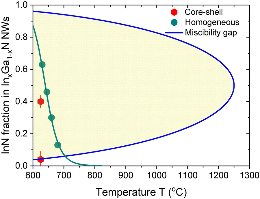 | ||
| Fig. 4 Miscibility gap in InxGa1−xN alloy as a function of temperature, which closes at 1250 °C (ref. 23). Temperature-dependent compositions of homogeneous InxGa1−xN NWs obtained by HVPE (symbols), fitted by the LM model (line),26 are entirely within the miscibility gap. The InN fraction in the cores of our InxGa1−xN NWs (x = 0.4) is also within the miscibility gap, while the composition of the shells (x = 0.04) lies at its border. | ||
Spontaneous formation of optically effective core–shell structures in InGaN NWs without any change in the Ga/In flux ratio or group III flux commutation is more surprising and interesting. It was never reported for catalyst-free III–V ternary NWs to our knowledge. Spontaneous core–shell structures were earlier demonstrated only in VLS NWs (for example, in AlGaAs NWs with Au droplets34–36), and attributed to different growth mechanisms of the VLS core and the vapor–solid shell that forms after the core.36 The absence of visible droplets on top of our NWs (which simply cannot form under N-rich growth conditions in vapor) rules out this explanation. To understand the phenomenon, we recall the mononuclear growth mechanism of single MLs on top of NWs. Such growth, with a time-scale hierarchy between an almost instantaneous ML progression and slow refill from vapor, was discussed in detail for VLS III–V binary NWs. It has far reaching implications in their morphology, crystal phase and statistical properties.37–45 According to ref. 46 and 47 selective area growth of hexahedral GaAs NWs (∼100 nm in radius), and elongated GaAs nanomembranes (∼20 μm in length and 125–270 nm in thickness) is also mononuclear. However, mononuclear growth and its effect on the NW composition were never considered for III–V ternary NWs.
4. Modeling
We speculate that the sharp transition from the In-rich core to the Ga-rich shell is due to the periodically changing local environment in mononuclear growth of single MLs on top of NWs. We assume that NW MLs nucleate in the center of NWs, where the surface concentration of group III and V adatoms is lowest. At nucleation and in the initial stage of ML progression, the adatom sea around an island can be either N-rich, or balanced, or only slightly group III rich. This corresponds to the N-rich vapor environment and higher volatility of N atoms. Partial ML evolves instantaneously, consuming available adatoms without refill from vapor in this time scale. N adatoms are able to diffuse over shorter distance compared to In and Ga adatoms, as in ref. 48 and 49 for As atoms. At a certain ML size, most N adatoms are collected from the surrounding surface, and the growth conditions for further ML progression become group III rich. This growth behavior is schematized in Fig. 5(a). | ||
| Fig. 5 (a) Illustration of the ML growth process, with an In-rich core forming under a balanced local environment for partial ML (sufficient N), and Ga-rich shell forming under highly group III rich conditions (insufficient N). (b) Vapor–solid distributions of InxGa1−xN NWs at 625 °C, obtained from eqn (3) and (5) with ω = 3.39, β = 0.45, α0 = 0.73, k = 4.5, and different ML sizes r for a NW radius R of 50 nm. The initial distribution in the NW center is close-to-linear. Any composition of the core can be achieved by tuning the In content in the vapor. Due to insufficient amount of N adatoms, the growth conditions for the instantaneous ML progression in the shell region become group III rich. This develops the miscibility gaps, corresponding to the wavy sections in the vapor–solid distributions at larger r. The red line shows the equilibrium distribution. (c) Fit to the data by eqn (6) at z = 0.5. (d) Interfacial profiles at different z, showing that different InN fractions in the NW core can be obtained by tuning the vapor composition. | ||
According to ref. 50 the vapor–solid distribution of III–V ternary materials based on group III intermix at c ≅ 1 is given by
| z = x, α > 1, |
| z = αx + (1 − α)F(x), α ≤ 1, |
 | (3) |
 | (4) |
Group III and N adatoms are collected from different lengths. The diffusion length of group V adatoms is shorter than for In and Ga adatoms.32,48,49 As a result, the effective V/III ratio is lower than the V/III flux ratio in vapor F53 = 2IN2/(IIn + IGa), with 2IN2 as the vapor flux of N2 dimers and Ij as the atomic vapor fluxes of j = In and Ga. The balanced growth at α = 1, or group V rich growth at α > 1 yield the purely kinetic distribution z = x. In this regime, any In or Ga adatom arriving to the ML boundary finds its N adatom and incorporates into the solid. Group III rich growth at α ≪ 1 yields the close-to-equilibrium distribution z ≅ F(x). This is due to the excess of In and Ga adatoms that must desorb in the absence of N adatoms available for crystallization.
The local environment for single ML growth changes with its linear size r (0 ≤ r ≤ R, with R as the NW radius) in favor of group III rich conditions. In the first approximation in r, the local V/III ratio should decrease from its initial value α0 at nucleation according to α = α0[1 − k(r/R)2], with a relaxation coefficient k. Further evolution of α depends on many factors including the diffusion lengths of different adatoms on the NW top facet and sidewalls, re-emission, NW radius and surface density. This complex problem requires a separate study and comparison with the compositional data for different NW geometries, In fractions in vapor and total V/III flux ratios. Here, we use the exponential approximation
| α = α0e−k(r/R)2, | (5) |
 | (6) |
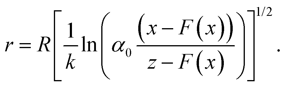
Fig. 5(b) shows the vapor–solid distributions across the core–shell InxGa1−xN NWs at different r, obtained from eqn (3) and (5) at ω = 3.39, β = 0.45, α0 = 0.73 and k = 4.5, for a NW radius R of 50 nm. The curves are transitioned from close-to-linear at r = 0 to the wavy shapes at larger r. The miscibility gap is suppressed in the core (r ≤ 20 nm), but not in the shell (r > 20 nm). Fig. 5(c) shows the excellent fit to the compositional profile with these parameters at z = 0.5. The distance d equals d = r ± 50 nm, with r = 0 corresponding to the NW center. Finally, Fig. 5(d) shows the compositional profiles at different z, and demonstrates that the composition of In-rich cores can be finely tuned by changing the vapor composition. The sharp interfaces of spontaneous core–shell heterostructures in InxGa1−xN NWs is well reproduced within the model.
According to this analysis, the mechanism of spontaneous core–shell formation in InxGa1−xN NWs is quasi-instantaneous growth of single NW MLs without refill from vapor. In this process, the total amounts of group III and N atoms available for ML growth are fixed at nucleation, and cannot be changed by vapor fluxes. At the beginning of ML formation, the growth conditions are balanced by slightly N-rich vapor. The NW core forms in the kinetic regime, where almost group III atoms incorporate into the solid. This leads to the kinetic suppression of the miscibility gap. The InN fraction in the solid (0.4) is close to the In content in the vapor (0.5). When most N atoms from the pre-existing reservoir are used for ML growth, group III atoms can no longer incorporate into the solid. The ML growth conditions become equilibrium for both In and Ga adatoms. As a result, the thermodynamically forbidden miscibility gap manifests in the reduced fraction of InN in the shell. The transition region is narrow due to a wide miscibility gap at 625 °C. This results in an abrupt heterointerface between the optically active core and the barrier shell. The model quantifies this behavior and predicts its general character in nanostructures that grow from a confined mother phase.
5. Conclusion
In summary, we have demonstrated spontaneous core–shell heterostructures in InxGa1−xN NWs grown on Si(111) substrates by MBE at 625 °C. The In content in vapor was fixed at 0.5. 20 nm radius cores had an InN fraction of ∼0.4, which was reduced to ∼0.04 in 30 nm thick shells, with abrupt heterointerfaces. In-rich cores demonstrated bright PL at 650 nm, with linear dependence of the integral PL intensity on the excitation power density. Such structures should be useful for III-nitride based red lasers, RGB LEDs, and color-tunable light sources. The effect of spontaneous formation of core–shell heterostructures in catalyst-free InGaN NWs was explained by periodically changing the local environment for quasi-instantaneous growth of single MLs on top of NWs. The growth conditions change from balanced at the beginning to group III rich at the end of ML growth. Consequently, the miscibility gap is suppressed in the core but present in the shell. The role of instantaneous growth of single MLs in III–V ternary NWs and the very possibility of the spontaneous material separation in catalyst-free nanostructures is described here for the first time to our knowledge. A similar effect can occur in other III–V NWs grown by the VLS or catalyst-free mechanisms. Overall, these results provide a simple method for the fabrication of optically active NW heterostructures in the extended wavelength range.Author contributions
V. G. D. handled the modeling and wrote the theoretical section of the manuscript. All other authors contributed equally to various aspects of the experimental work (MBE growth, structural and optical characterization, chemical analysis) and writing the experimental sections of the manuscript. All authors commented on the work and approved the final version of the manuscript.Data availability
Data are contained within the article.Conflicts of interest
There are no conflicts to declare.Acknowledgements
Growth experiments and optical measurements were carried out with financial support of the Russian Science Foundation (Project No. 23-79-00012). Structural properties were studied under the support of the Ministry of Science and Higher Education of the Russian Federation (State task No. 0791-2023-0004). VGD gratefully acknowledges the research grant of St. Petersburg State University (ID 95440344) for financial support of modeling. PL studies were carried out using the equipment of the large-scale research facility “Complex optoelectronic stand”.References
- P. J. Parbrook, B. Corbett, J. Han, T.-Y. Seong and H. Amano, Micro-light emitting diode: From chips to applications, Laser Photonics Rev., 2021, 15, 200013 CrossRef.
- T. R. Kuykendall, A. M. Schwartzberg and S. Aloni, Gallium nitride nanowires and heterostructures: Toward color-tunable and white-light sources, Adv. Mater., 2015, 27, 5805 CrossRef CAS.
- A. Pandey, J. Min, M. Reddeppa, Y. Malhotra, Y. Xiao, Y. Wu, K. Sun and Z. Mi, An ultrahigh efficiency excitonic micro-LED, Nano Lett., 2023, 23, 1680 CrossRef CAS.
- Y.-H. Ra and C. R. Lee, Core–shell tunnel junction nanowire white-light-emitting diode, Nano Lett., 2020, 20, 4162 CrossRef CAS.
- X. Pan, J. Song, H. Hong, M. Luo and R. Nötzel, Red InGaN nanowire LED with bulk active region directly grown on p-Si(111), Opt. Express, 2023, 31, 15772 CrossRef CAS.
- P. K. Saha, K. S. Rana, N. Thakur, B. Parvez, S. A. Bhat, S. Ganguly and D. Saha, Room temperature single-photon emission from InGaN quantum dot ordered arrays in GaN nanoneedles, Appl. Phys. Lett., 2022, 121, 211101 CrossRef CAS.
- C. Thota, M. Reddeppa, K. Sairam Pasupuleti, D.-J. Nam, N.-H. Bak, Y. H. Kim, S.-G. Kim and M.-D. Kim, Feather-shaped InGaN nanorods for selective ppb-level detection of NO2 gas at room temperature, ACS Appl. Nano Mater., 2021, 4, 13288 CrossRef CAS.
- F. Z. Tijent, P. Voss and M. Faqir, Recent advances in InGaN nanowires for hydrogen production using photoelectrochemical water splitting, Mater. Today, 2023, 33, 101275 CAS.
- F. Glas, Critical dimensions for the plastic relaxation of strained axial heterostructures in free-standing nanowires, Phys. Rev. B: Condens. Matter Mater. Phys., 2006, 74, 121302 CrossRef.
- L. C. Chuang, M. Moewe, C. Chase, N. P. Kobayashi, C. Chang-Hasnain and S. Crankshaw, Critical diameters for III–V nanowires grown on lattice-mismatched substrates, Appl. Phys. Lett., 2007, 90, 043115 CrossRef.
- P. C. McIntyre and A. Fontcuberta, i Morral, Semiconductor nanowires: to grow or not to grow? Mater. Today, NANO, 2020, 9, 100058 Search PubMed.
- S. D. Hersee, A. K. Rishinaramangalam, M. N. Fairchild, L. Zhang and P. Varangis, Threading defect elimination in GaN nanowires, J. Mater. Res., 2011, 26, 2293 CrossRef CAS.
- M. A. Sanchez-Garcia, E. Calleja, E. Monroy, F. J. Sanchez, F. Calle, E. Muñoz and R. J. Beresford, The effect of the III/V ratio and substrate temperature on the morphology and properties of GaN- and AlN-layers grown by molecular beam epitaxy on Si(111), J. Cryst. Growth, 1998, 183, 23 CrossRef CAS.
- R. K. Debnath, R. Meijers, T. Richter, T. Stoica, R. Calarco and H. Lüth, Mechanism of molecular beam epitaxy growth of GaN nanowires on Si, Appl. Phys. Lett., 2007, 90, 123117 CrossRef.
- V. Consonni, M. Hanke, M. Knelangen, L. Geelhaar, A. Trampert and H. Riechert, Nucleation mechanisms of self-induced GaN nanowires grown on an amorphous interlayer, Phys. Rev. B: Condens. Matter Mater. Phys., 2011, 83, 035310 CrossRef.
- R. Songmuang, T. Ben, B. Daudin, D. Gonzalez and E. Monroy, Identification of III–N nanowire growth kinetics via a marker technique, Nanotechnology, 2010, 21, 295605 CrossRef CAS.
- M. Sobanska, S. Fernández-Garrido, Z. R. Zytkiewicz, G. Tchutchulashvili, S. Gieraltowska, O. Brandt and L. Geelhaar, Self-assembled growth of GaN nanowires on amorphous AlxOy: From nucleation to the formation of dense nanowire ensembles, Nanotechnology, 2016, 27, 325601 CrossRef CAS.
- K. D. Goodman, V. V. Protasenko, J. Verma, T. H. Kosel, H. G. Xing and D. Jena, Green luminescence of InGaN nanowires grown on silicon substrates by molecular beam epitaxy, J. Appl. Phys., 2011, 109, 084336 CrossRef.
- C.-C. Hong, H. Ahn, C.-Y. Wu and S. Gwo, Strong green photoluminescence from InxGa1−xN/GaN nanorod arrays, Opt. Express, 2009, 17, 17227 CrossRef CAS.
- V. O. Gridchin, K. P. Kotlyar, R. R. Reznik, A. S. Dragunova, N. V. Kryzhanovskaya, V. V. Lendyashova, D. A. Kirilenko, I. P. Soshnikov, D. S. Shevchuk and G. E. Cirlin, Multi-colour light emission from InGaN nanowires monolithically grown on Si substrate by MBE, Nanotechnology, 2021, 32, 335604 CrossRef CAS.
- I. Ho and G. Stringfellow, Solid phase immiscibility in GaInN, Appl. Phys. Lett., 1996, 69, 2701 CrossRef CAS.
- Y. Kanagawa, T. Ito, Y. Kumagai and A. Koukitu, Thermodynamic study on compositional instability of InGaN/GaN and InGaN/InN during MBE, Appl. Surf. Sci., 2003, 216, 453 CrossRef.
- J. Adhikari and D. Kofke, Molecular simulation study of miscibility of ternary and quaternary InGaAlN alloys, J. Appl. Phys., 2004, 95, 6129 CrossRef CAS.
- C.-Z. Ning, L. Dou and P. Yang, Bandgap engineering in semiconductor alloy nanomaterials with widely tunable compositions, Nat. Rev. Mater., 2017, 2, 17070 CrossRef CAS.
- T. Kuykendall, P. Ulrich, S. Aloni and P. Yang, Complete composition tunability of InGaN nanowires using a combinatorial approach, Nat. Mater., 2007, 6, 951 CrossRef CAS.
- E. Roche, Y. Andre, G. Avit, C. Bougerol, D. Castelluci, F. Reveret, E. Gil, F. Medard, J. Leymarie, T. Jean, V. G. Dubrovskii and A. Trassoudain, Circumventing the miscibility gap in InGaN nanowires emitting from blue to red, Nanotechnology, 2018, 29, 465602 CrossRef.
- M. Zeghouane, G. Avit, Y. André, C. Bougerol, Y. Robin, P. Ferret, D. Castelluci, E. Gil, V. G. Dubrovskii, H. Amano and A. Trassoudaine, Compositional control of homogeneous InGaN nanowires with the In content up to 90%, Nanotechnology, 2019, 30, 044001 CrossRef CAS.
- X. Zhang, B. Haas, J.-L. Rouviere, E. Robin and B. Daudin, Growth mechanism of InGaN nano-umbrellas, Nanotechnology, 2016, 27, 455603 CrossRef.
- V. O. Gridchin, K. P. Kotlyar, E. V. Ubyivovk, V. V. Lendyashova, A. S. Dragunova, N. V. Kryzhankovskaya, D. S. Shevchuk, R. R. Reznik, S. A. Kukushkin and G. E. Cirlin, Growth of three-dimensional InGaN nanostructures by plasma-assisted molecular beam epitaxy, ACS Appl. Nano Mater., 2024, 7, 17460 CrossRef CAS.
- V. Gridchin, S. Komarov, I. Soshnikov, I. Shtrom, R. Reznik, N. Kryzhanovskaya and G. Cirlin, On the growth of InGaN nanowires by molecular-beam epitaxy: Influence of the III/V flux ratio on the structural and optical properties, J. Surf. Invest.: X-Ray, Synchrotron Neutron Tech., 2024, 18, 408 CrossRef CAS.
- R. Deng, X. Pan, H. Hong, G. Yang, X. Pu, J. Song and R. Nötzel, Transition from metal-rich to N-rich growth for core−shell InGaN nanowires on Si (111) at the onset of In desorption, Cryst. Growth Des., 2024, 24, 414 CrossRef CAS.
- M. Morassi, L. Largeau, F. Oehler, H.-G. Song, L. Travers, F. H. Julien, J. C. Harmand, Y.-H. Cho, F. Glas, M. Tchernycheva and N. Gogneau, Morphology tailoring and growth mechanism of indium-rich InGaN/GaN axial nanowire heterostructures by plasma-assisted molecular beam epitaxy, Cryst. Growth Des., 2018, 18, 2545 CrossRef CAS.
- V. G. Dubrovskii, Composition of vapor–liquid–solid III–V ternary nanowires based on group III intermix, Nanomaterials, 2023, 13, 2532 CrossRef CAS.
- C. Chen, S. Shehata, C. Fradin, R. R. LaPierre, C. Couteau and G. Weihs, Self-directed growth of AlGaAs core–shell nanowires for visible light applications, Nano Lett., 2007, 7, 2584 CrossRef CAS.
- S. K. Lim, M. J. Tambe, M. M. Brewster and S. Gradečak, Controlled growth of ternary alloy nanowires using metalorganic chemical vapor deposition, Nano Lett., 2008, 8, 1386 CrossRef CAS.
- V. G. Dubrovskii, I. V. Shtrom, R. R. Reznik, Yu. B. Samsonenko, A. I. Khrebtov, I. P. Soshnikov, S. Rouvimov, N. Akopian, T. Kasama and G. E. Cirlin, Origin of spontaneous core–shell AlGaAs nanowires grown by molecular beam epitaxy, Cryst. Growth Des., 2016, 16, 7251 CrossRef CAS.
- F. Glas, J. C. Harmand and G. Patriarche, Nucleation antibunching in catalyst-assisted nanowire growth, Phys. Rev. Lett., 2010, 104, 135501 CrossRef.
- C. Y. Wen, J. Tersoff, K. Hillerich, M. C. Reuter, J. H. Park, S. Kodambaka, E. A. Stach and F. M. Ross, Periodically changing morphology of the growth interface in Si, Ge, and GaP nanowires, Phys. Rev. Lett., 2011, 107, 025503 CrossRef.
- J. C. Harmand, G. Patriarche, F. Glas, F. Panciera, L. Florea, J.-L. Maurice, L. Travers and Y. Ollivier, Atomic step flow on a nanofacet, Phys. Rev. Lett., 2018, 121, 166101 CrossRef CAS.
- F. Panciera, Z. Baraissov, G. Patriarche, V. G. Dubrovskii, F. Glas, L. Travers, U. Mirsaidov and J. C. Harmand, Phase selection in self-catalyzed GaAs nanowires, Nano Lett., 2020, 20, 1669 CrossRef CAS.
- V. G. Dubrovskii, Refinement of nucleation theory for vapor–liquid–solid nanowires, Cryst. Growth Des., 2017, 17, 2589 CrossRef CAS.
- F. Glas, F. Panciera and J. C. Harmand, Statistics of nucleation and growth of single monolayers in nanowires: Towards a deterministic regime, Phys. Status Solidi RRL, 2022, 16, 2100647 CrossRef CAS.
- F. Glas, Incomplete monolayer regime and mixed regime of nanowire growth, Phys. Rev. Mater., 2024, 8, 043401 CrossRef CAS.
- F. Glas and V. G. Dubrovskii, Energetics and kinetics of monolayer formation in vapor–liquid–solid nanowire growth, Phys. Rev. Mater., 2020, 4, 083401 CrossRef CAS.
- E. Koivusalo, T. Hakkarainen, M. D. Guina and V. G. Dubrovskii, Sub-Poissonian narrowing of length distributions realized in Ga-catalyzed GaAs nanowires, Nano Lett., 2017, 17, 5350 CrossRef CAS.
- M. Zendrini, V. G. Dubrovskii, A. Rudra, D. Dede, A. Fontcuberta, I. Morral and V. Piazza, Nucleation-limited kinetics of GaAs nanostructures grown by selective area epitaxy: Implications for shape engineering in optoelectronic devices, ACS Appl. Nano Mater., 2024, 7, 19065 CrossRef CAS.
- V. G. Dubrovskii, Nucleation-dependent surface diffusion in anisotropic growth of III–V nanostructures, Cryst. Growth Des., 2024, 24, 6450 CrossRef CAS.
- A. Pishchagin, F. Glas, G. Patriarche, A. Cattoni, J. C. Harmand and F. Oehler, Dynamics of droplet consumption in vapor–liquid–solid III–V nanowire growth, Cryst. Growth Des., 2021, 21, 4647 CrossRef CAS.
- D. Mosiiets, Y. Genuist, J. Cibert, E. Bellet-Amalric and M. Hocevar, Dual-adatom diffusion-limited growth model for compound nanowires: Application to InAs nanowires, Cryst. Growth Des., 2024, 24, 3888 CrossRef CAS.
- V. G. Dubrovskii and E. D. Leshchenko, Composition of III–V ternary materials under arbitrary material fluxes: the general approach unifying kinetics and thermodynamics, Phys. Rev. Mater., 2023, 7, 074603 CrossRef CAS.
| This journal is © The Royal Society of Chemistry 2024 |