 Open Access Article
Photoemission spectroscopy and microscopy for Ta@Si16 superatoms and their assembled layers†
Masahiro
Shibuta‡
 a,
Tsutomu
Ohta
b,
Toshiaki
Kamoshida
b,
Kana
Yamagiwa
b,
Hironori
Tsunoyama
b,
Tomoya
Inoue
b,
Tsugunosuke
Masubuchi
 b and
Atsushi
Nakajima
 *ab
*ab
aKeio Institute of Pure and Applied Sciences (KiPAS), Keio University, 3-14-1 Hiyoshi, Kohoku-ku, Yokohama 223-8522, Japan. E-mail: nakajima@chem.keio.ac.jp; Fax: +81-45-566-1697; Tel: +81-45-566-1712
bDepartment of Chemistry, Faculty of Science and Technology, Keio University, 3-14-1 Hiyoshi, Kohoku-ku, Yokohama 223-8522, Japan
First published on 29th October 2024
Abstract
Superatoms (SAs) with specific compositions have the potential to significantly advance the field of nanomaterials science, leading to next-generation nanoscale functionalities. In this study, we fabricated assembled layers with tantalum metal-atom encapsulating silicon cage (Ta@Si16) SAs on an organic C60 substrate through deposition, and we characterized their electronic and optical properties by photoelectron spectroscopy and microscopy. The alkaline nature of Ta@Si16 SAs reveals their electronic behaviors, such as charge transfer and electromagnetic near-field sensing, through two-photon photoemission (2PPE) spectroscopy and microscopy with a femtosecond laser. The evolution of the work function for Ta@Si16 SAs on C60, observed by 2PPE spectroscopy, demonstrates charge transfer complexation between the topmost C60 layer and the first Ta@Si16 layer, consistent with the electron-donating alkaline characteristics of Ta@Si16 SAs. Specifically, a small amount of Ta@Si16 SA deposition leads to a dramatic increase in 2PPE intensity, attributable to electromagnetic near-field enhancements, suggesting applications as sensitizers for nonlinear imaging in photoemission microscopy. For the assembled Ta@Si16 SA layers, a plasmonic response of hνp = 17.9 eV is spectroscopically identified, including their valence and conduction band structures, and the plasmonic energetics are discussed in the context of metal doping in bulk silicon.
1. Introduction
Nanoclusters (NCs) with countable numbers of atoms are promising functional materials for future electronic and optical devices. Among the vast combinations of atomic species and their numbers, stably existing NCs with specific atomic compositions have been identified as “superatoms” (SAs),1–8 whose characteristic stabilities are governed by geometric and electronic factors. Following the discovery of fullerenes as SAs,9 extensive research has been conducted on X@Al12 (X = B and Al)10–13 and metal-encapsulating silicon cage (M@Si16) SAs14–21 in the gas phase, leading to the exploration of ligated metal NCs, such as Aun(SR)m,22–26 in the liquid phase.M@Si16 SAs, in particular, are of potential interest as silicon-based nanomaterials, where their electronic properties can be tuned by endohedral doping of central metal atoms in a common Si caged structure (Fig. 1 inset). According to the 68-electron counting rule in SAs (4e− × 16 for the Si cage and ne− for the central metal atom), M@Si16 SAs with group 4 metals (n = 4; Ti, Zr, and Hf) exhibit electronically insulating properties due to electron shell closures, behaving as intrinsic semiconductors. By substituting the central metal with group 3, 5, and 6 metals (n = 3; Sc, Y, Lu, n = 5; V, Nb, Ta, and n = 6; Cr, Mo, W), they acquired n-type (n = 3) and p-type (n = 5 and 6) characteristics with a deficiency or surplus of electron(s).14,17,20,21
When non-ligated SAs generated in the gas phase are deposited on a substrate, a chemical interaction between the SAs and the substrate occurs, resulting in their favorable charge states.27–36 The molecularly local electronic structure resulting from this interaction governs the charge injection/ejection properties at the hetero-interface. Furthermore, in films with deposited SAs, chemical interactions between neighbouring SAs provide additional functionalities, such as electric conduction and charge separation properties.37,38 To further understand and control functional systems based on SAs, it is important to characterize the electronic and optical properties of SA layers/films grown on substrates.
Over the past decade, significant advancements have been made in the precise synthesis and deposition of atomically mass-selected NCs, including SAs,27–36 where the deposited NCs/SAs on substrates have been characterized by conventional methods for materials science (e.g., photoelectron spectroscopy,27–36 scanning tunnelling microscopy (STM),39,40 and X-ray absorption fine structure (EXAFS)).41 Recent developments in size-selected NC deposition methodologies have addressed the abovementioned fundamental issues; the flux of an atomically mass-selected SA beam now allows for the fabrication of SA multilayers on substrates within a realistic timeframe (within several hours of operation), with a beam flux comparable to that of the molecular beam epitaxy (MBE) method used to form highly crystalline inorganic/organic epitaxial films.42 The electronic conduction properties of size-selected SA films have been characterized, revealing their potential utility in functional nanodevices.43,44
In the initial stage of SA film growth on substrates, M@Si16 SAs have been found to be stably immobilized on organic substrates by appropriately selecting their molecular properties (e.g. p- or n-type); positively or negatively charged SAs are stabilized with p- or n-type molecular characteristics, leading to molecularly favourable charge transfer interactions at their interfaces.27–36 While pure M@Si16 SA films have been shown to be tolerant to the ambient environment when protected by an overlayer,42 the collective electronic/optical behaviors of assembled M@Si16 SA layers remain uncharacterized beyond the nature of locally immobilized SAs.
In this study, we have characterized the electronic structures of p-type Ta@Si16 SA layers grown on an organic n-type C60 fullerene substrate by detecting photoelectrons excited by different light sources. During the initial stage of depositing a small amount of Ta@Si16 SAs (section 3.1), ranging from sub-monolayer to several monolayers (MLs), we focus on the interfacial characteristics of electronically excited states and changes in the work function (section 3.1.1),45–49 using two-photon photoemission (2PPE) spectroscopy with a femtosecond light source. The quantitative evolution of the work function with increasing SA coverage (section 3.1.2) demonstrates the formation of an adsorption-induced surface dipole at the interface between the first layer of the p-type (or alkaline-like) Ta@Si16 SA and the n-type C60 substrate due to charge transfer interactions. Furthermore, 2PPE spectroscopy resolves the photoexcited electrons in the conduction band of the Ta@Si16 SA layer (section 3.1.3), while the 2PPE intensity is dramatically enhanced by the characteristic nonlinear optical responses of Ta@Si16 SAs, indicating that the optical responses can be used as sensitizers for nonlinear microscopic imaging to visualize surface plasmon polariton (SPP) propagation at buried metal–dielectric interfaces (section 3.1.4). For thicker assembled Ta@Si16 SA layers, with up to 7 MLs (section 3.2), we further characterized the chemical state and plasmonic response of the SA film by X-ray photoelectron spectroscopy (XPS) (section 3.2.1). The plasmon excitation of these SA layers, influenced by metal-atom encapsulation, differs from that of pure bulk Si crystals. Ultraviolet photoelectron spectroscopy (UPS) and 2PPE spectroscopy provide insights into electronic structures both below and above the Fermi level (EF), with the experimental observations further supported by DFT calculations (section 3.2.2).
2. Experimental section
2.1. Fabrication of the Ta@Si16 SA film on a C60 substrate
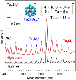
The Ta@Si16 SA film was prepared using a magnetron sputtering (MSP) NC deposition method, with the detailed methodology described elsewhere.29,30,50 In brief, Ta and Si atoms evaporated by Ar ion sputtering aggregate into NCs in cooled He gas. The charged NCs, including SAs, are introduced into a quadrupole mass filter using ion optics. Fig. 1 shows the mass spectra of the cationic Ta–Si binary NCs synthesised with the MSP source using a Ta–Si mixed target. The high-resolution mode spectrum (bottom spectrum) shows a prominent peak at m/z = 630, corresponding to the Ta@Si16 SA, indicating its magic number behavior. The neighbouring product peaks, Si22 (m/z = 616) and Ta2Si10 (m/z = 642), are well-separated from the Ta@Si16 SA peak and are weak (a few %) compared to the dominant SA production. The targeted pure Ta@Si16 SA can then be deposited in high-transmission mode (top spectrum), with an organic substrate placed at the throughput of a Q-mass filter, fixing the potentials of the electrodes in the mass filter for a specific mass number (m/z = 630 for the Ta@Si16 SA). The flux of the SA beam is sufficient to reach several nA (6.2 × 10⁹ SAs per nA per s) in the latest development, enabling the preparation of a 1 ML Ta@Si16 SA film (corresponding to 5 × 10¹³ SAs; see ESI Note S1 and Fig. S1†) on a substrate within 1 hour of operation.Since the Ta@Si16 SA has p-type character (68 electron shell closure in a cationic state), an n-type organic substrate is plausible.28,30,31–33 Here, we chose an n-type C60 substrate, prepared by vacuum deposition on a graphite-based solid just before SA deposition. The C60 thickness was 2 MLs, sufficient to electronically decouple the SA from the graphite. We also prepared a thick C60 substrate (10 MLs) on a plasmonic gold (Au) (111) substrate, demonstrating the visualization of lateral plasmonic excitation51–58 at the C60/Au(111) interface sensitized by SA deposition (see section 3.1.4). The C60 substrates were immediately transferred to the SA deposition system without disrupting the ultrahigh vacuum conditions.
2.2. Photoelectron spectroscopy and microscopy
The growth of the SA film and its electronic properties were evaluated using a photoelectron spectroscopy system (VG Scienta R-3000) with various photon sources, including XPS, UPS, and 2PPE. In XPS, an MgKα characteristic X-ray source (photon energy, hν = 1253.6 eV) was used to extract photoelectrons from the core levels of the atoms in the sample. We set the detection takeoff angle to 45° for surface sensitivity. The instrumental resolution, evaluated by the Au 4f7/2 core level, was 1.12 eV, primarily governed by the intrinsic line width of the MgKα line.59 The binding energy was calibrated to the energy of the Au 4f7/2 peak at 84.0 eV.For UPS, a He I discharge lamp (hν = 21.22 eV) was employed to observe the valence electronic structures with high energy resolution (<30 meV). In the case of 2PPE spectroscopy, the third harmonics of a titanium sapphire laser (COHERENT: Mira 900-F) were generated and focused onto the sample surface with an aluminium concave mirror (f = 400 mm). 2PPE can observe the unoccupied electronic states (or conduction bands) above the EF with energy resolution comparable to that of UPS (30 meV).60–62 Due to the surface sensitivity in the region of photoelectron kinetic energy being sufficient, normal emission of photoelectrons was detected in both UPS and 2PPE spectroscopy. Furthermore, 2PPE spectroscopy is valuable for evaluating the work function, as the detection area is limited with respect to the spot size of the incident laser (approximately 0.1 mm in diameter). To avoid unexpected effects of the local work function on surface defects or impurities, we selected the probe area for obtaining reproducible spectral data.
We also employed photoelectron emission microscopy (PEEM; IS-PEEM, FOCUS GmbH) to image the lateral distribution of 2PPE, i.e. 2P-PEEM. As mentioned in section 3.1.4, plasmonic excitation and propagation at the metal/dielectric interface can be visualized using 2P-PEEM,51–58 where both fundamental and third harmonics of the titanium sapphire laser were irradiated onto the plasmonic sample with spatiotemporal overlap. The incident angle of the light source was 75° relative to the surface normal. The lateral resolution of the 2P-PEEM setup was better than 80 nm, depending on the extractor lens voltage of the PEEM optics.48,63,64 In general, 2P-PEEM images of inhomogeneous samples show significant photoemission signals from defects or impurities. In our case, however, no such “hot spots” were observed, confirming the uniformity of the sample. This uniformity was ensured by performing all experimental procedures and measurements within the UHV system.
3. Results and discussion
3.1. 2PPE spectroscopy and microscopy for Ta@Si16 SAs on C60 organic surfaces
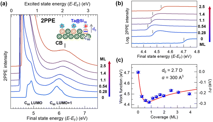 | ||
| Fig. 2 (a) Coverage-dependent 2PPE spectra (hν = 4.13 eV) of the Ta@Si16 SA on C60. The bottom and top axes represent the energies of the final state and the intermediately excited state with respect to the EF, respectively. Before SA deposition, the C60-derived LUMO and LUMO+1 levels are observed at EF + 0.8 eV and EF + 1.8 eV (see the top axis).61 The 2PPE intensity is significantly enhanced by SA deposition, especially at the lower energy. The low-energy cutoff of the 2PPE spectra in the final state energy corresponds to the vacuum level (=EF + work function). A peak at 6.2 eV in the final state energy is a conduction band (CB) structure of the SA film at EF + 2.1 eV (top axis). (b) Magnified 2PPE spectra at the low-energy cut off region on a logarithmic intensity scale. The work function (marked by vertical bars) decreases by 0.3 eV at lower coverages of up to 1 ML, while it slightly increases at coverages greater than 1 ML. (c) The coverage-dependent work function attributable to the electron-donating p-type (alkaline-like) properties of the Ta@Si16 SA, similar to alkaline atom deposition. The change in the work function, Δφ (right axis), is fitted using a Topping model66 with eqn (1), providing an adsorption-induced dipole moment, d0, of 2.7 D. | ||
Upon deposition of the Ta@Si16 SAs, the 2PPE intensity drastically increases, particularly in the lower energy region due to the nonlinear optical response of Ta@Si16 SAs (section 3.1.4). Furthermore, a new spectral feature appears at 6.2 eV in the final state energy. This photoemission signal originates from the conduction band electron at EF + 2.1 eV photoexcited in the Ta@Si16 SA film (section 3.2.2). In the low-energy cutoff region, the onset energy reveals the behaviors of the work function and shows coverage dependence; up to less than 1 ML, the cutoff energy shifts toward a lower energy, while it slightly increases at higher coverages.
Fig. 2(b) shows the magnified 2PPE spectra of Fig. 2(a) in the low-energy cutoff regions on a logarithmic intensity scale. With Ta@Si16 SA deposition up to less than 1 ML, the work function gradually decreases by approximately 0.3 eV from 4.7 to 4.4 eV, while it increases to about 4.5 eV at higher deposition amounts (>1 ML). More detailed work functions are plotted against the SA coverages, as shown in Fig. 2(c).
The characteristic change in the work function is closely associated with that of the well-studied adsorption behavior of alkaline atoms on metal or semiconductor substrates.66 This can be explained by: (1) a surface dipole layer formed by electron-donating alkaline adatoms on the substrate lowering the work function, (2) the dipole layer being lifted by depolarization at coverages approaching 1 ML, and (3) the work function slightly recovering at multilayer coverages. Therefore, our experimental results indicate that an adsorption-induced dipole layer forms at the first layer of the p-type (alkaline-like) Ta@Si16 SA film on C60, driven by interfacial charge transfer (inset in Fig. 2(a)).
More quantitatively, the change in the work function, Δφ (right axis in Fig. 2(c)), due to the formation of a surface dipole layer can be described by the Topping model66 as:
 | (1) |
As shown in the 2PPE spectra of Ta@Si16 SAs in the lower energy region (Fig. 2(a)), a dramatic enhancement of the 2PPE intensity is observed. Since the intensity enhancement is clearly recognizable even at sub-ML coverages, the 2PPE spectral feature does not merely reflect the density of states of the Ta@Si16 film itself. A plausible explanation for the intensity enhancement in the 2PPE spectra is the nonlinear optical response (e.g. nonlinear scattering) of Ta@Si16 SAs, where 2PPE sensitively responds to the generated near-field with the nonlinear optical response. In fact, no photoemission enhancement occurs in UPS using the a cw discharge lamp; the UPS intensity is rather suppressed by Ta@Si16 deposition due to the large difference in the ionization cross-sections between the C 2p- and Si 3p-derived valence electrons.70 Similar 2PPE enhancements have been reported in plasmonic silver nanoparticle/NC-deposited surfaces around their photoexcitation energies of localized surface plasmon resonance.48,55 The present results show that the Si-based SA can serve as a sensitive probe of nonlinear optical phenomena at the surface and/or interface, demonstrating its capability as a photo-sensitizer as described in the next section.
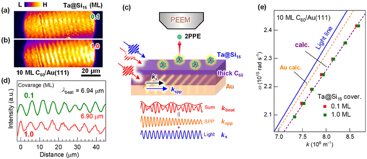
To address this issue, Ta@Si16 SAs deposited on a plasmonic C60/Au system are useful for effectively converting the near-field generated by propagating SPPs into nonlinear photoemission. Fig. 3(a) and (b) show the two-color 2P-PEEM (NIR: hν = 1.44 eV and UV: hν = 4.32 eV) images of 10 ML C60/Au decorated with (a) 0.1 ML and (b) 1 ML Ta@Si16 SAs. Fringe patterns propagating from an intrinsic groove are observed in 2P-PEEM. Such characteristic fringe patterns in 2P-PEEM were first observed by Kubo et al.71 for a silver thin film deposited on a mica substrate. The patterns result from the surface polarization beats formed by the interference between the electromagnetic fields induced by propagating SPPs and the remaining light. In the present 2P-PEEM, incident NIR photons form polarisation beats with SPP excitation at the C60/Au interface, and the interference fringe patterns are imaged by 2P-PEEM, where nonlinear photoemission from the Ta@Si16 SAs is induced simultaneously by illuminated UV photons,48,54,55,72 as schematically illustrated in Fig. 3(c). We would like to reiterate that no imaging of the buried SPPs at the C60/Au interface is available without decorating Ta@Si16 SAs; Ta@Si16 SAs play the role of sensitizers for the nonlinear photoelectron source accompanied by SPP propagation at the interface.
The lateral period of the beat patterns in 2P-PEEM (λbeat = 2π/kbeat) sensitively reflects the physical properties of SPPs (Fig. 3(d)), which are largely perturbed by the overlayered dielectric films. In turn, SA-sensitized SPP imaging is a powerful method to characterize the SPPs propagating at the buried interface. The wave vector of SPPs, kspp, excited by an incident photon (hν = hc/λ0 = hck0/2π, where c is the speed of light) at the dielectric/metal interface can be experimentally evaluated by kspp = kbeat + k0, which was found to be 7.49 × 10⁶ m−1 at hν = 1.44 eV. On the other hand, kspp can be simulated using an extended Drude model described by Kretschmann's equation:73
 | (2) |
The fringe pattern due to SPP propagation becomes more obvious at the higher Ta@Si16 coverage of 1 ML (Fig. 3(b)). As seen in the vertical line profile along with the kx (Fig. 3(d)), the λbeat is mostly independent of the Ta@Si16 coverage at least up to 1 ML. The above results clearly demonstrate that the Ta@Si16 SAs have the capability to visualize the surface near-field penetrated from the buried plasmonic interface with negligible perturbations of their physical properties.
Furthermore, 2P-PEEM provides important information about the SPP properties at the interface, namely the SPP dispersion and velocities. These physical properties of SPPs at the buried interface have been challenging to evaluate experimentally. Fig. 3(e) shows the SPP dispersion (ω versus kspp) evaluated by the λbeat obtained from 2P-PEEM at various photon energies (NIR; hν = 1.41–1.54 eV). The dispersion curve is in excellent agreement with the curve calculated using eqn (2). The phase and group velocities of SPPs can also be extracted from ω/k and dω/dk, which were found to be 0.96–0.98 c and 0.89 c, respectively.
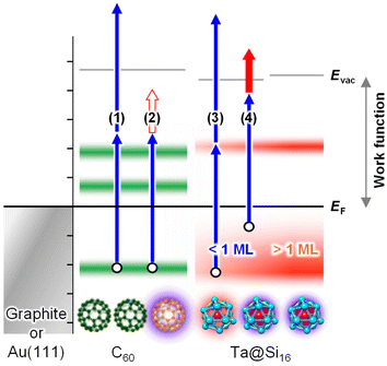
To summarize the electronic characterization and plasmonic sensitization of Ta@Si16 SAs, the energy diagram and excitation schemes with UV-UV and UV-NIR photons are illustrated in Fig. 4. Irradiation with SPP-exciting NIR and UV photons alone cannot energetically extract photoelectrons from the C60 surface (process (2) in Fig. 4). However, upon decorating with Ta@Si16 SAs, 2PPE with NIR-UV photons becomes effective (process (4) in Fig. 4; see also ESI Fig. S4† for the two-color 2PPE spectra), and its lateral distribution reflects the SPP-induced near-field at the surface. Notably, the enhancement of nonlinear photoemission from the Ta@Si16 SAs offers additional significant physical insights from the perspective of silicon plasmonics, where pure Si nanoparticles show no plasmonic response in the NIR or visible regions. In fact, the Ta@Si16 film shows a density of states just below the EF level (see Fig. 7), indicating the presence of free electrons capable of oscillating with an external electromagnetic field, i.e., localized surface plasmons. These optical and plasmonic responses of such a “metal-doped Si nanoparticle” represent an exciting frontier that will be explored in the near future.
3.2. Electronic characterization of Ta@Si16 SA thick films
![[thin space (1/6-em)]](https://www.rsc.org/images/entities/char_2009.gif) :
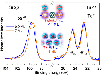
:![[thin space (1/6-em)]](https://www.rsc.org/images/entities/char_2009.gif) 16 for Ta@Si16 SAs.27,28 Furthermore, the XPS peak profiles of Si 2p and Ta 4f are mostly reproduced by considering uniform chemical components within the instrumental peak broadening (1.12 eV FWHM), indicating that the Ta@Si16 SA is deposited on the C60 substrate while preserving its caged structure through favorable charge transfer interaction, forming a Ta@Si16–C60 complex (see section 3.1.2).28 In addition, the coverage dependence of the C 1s peak shows a red shift by Ta@Si16 SA deposition up to the full coverage (1 ML). In fact, when a gold (Au) (111) single crystal is used as a substrate, the Si 2p core level shows multiple chemical components, caused by significant distortion of the SAs on the metal substrate (see ESI Fig. S5†).
16 for Ta@Si16 SAs.27,28 Furthermore, the XPS peak profiles of Si 2p and Ta 4f are mostly reproduced by considering uniform chemical components within the instrumental peak broadening (1.12 eV FWHM), indicating that the Ta@Si16 SA is deposited on the C60 substrate while preserving its caged structure through favorable charge transfer interaction, forming a Ta@Si16–C60 complex (see section 3.1.2).28 In addition, the coverage dependence of the C 1s peak shows a red shift by Ta@Si16 SA deposition up to the full coverage (1 ML). In fact, when a gold (Au) (111) single crystal is used as a substrate, the Si 2p core level shows multiple chemical components, caused by significant distortion of the SAs on the metal substrate (see ESI Fig. S5†).
For thick films, the XPS peak width of Si 2p becomes narrower compared to thin films, particularly with reduced intensity at the higher binding energy side. This peak narrowing results in an apparent peak shift (0.2 eV) toward a lower binding energy. Since the chemical state of the central Ta atom remains almost unchanged as Ta1+ (22.5 eV)28 regardless of the thickness, the spectral change in Si 2p indicates that the surrounding 16 Si atoms uniformly share a negative charge to compensate the overall charge of the Ta@Si16 SA, making it neutral in the multilayered film, i.e. Ta1+(Si16)1−. The charge states of the Ta@Si16 SA at 1 ML and in the multilayer films are schematically illustrated in the inset of Fig. 5.
When bare Ta@Si16 SAs accumulate and assemble into a multilayer, the inter-SA interactions should be induced by mixing the wave function with neighboring molecules, potentially leading to phenomena such as electric conduction43,44 or charge separation. Interestingly, these inter-SA interactions are evidently resolved by XPS in a wider energy scan, characterized as plasmonic responses of the Ta@Si16 SA layers. Fig. 6 shows the wide-range XPS spectra of the thin (0.6 ML) and thick (7 ML) Ta@Si16 films on the C60 substrate. Peaks at 117.2 eV and 41.6 eV appear in the thick film, where the energy separations from the main Si 2p and Ta 4f peaks are the same. The satellite peaks observed at the higher binding energies from the main core level peaks are associated with the energy loss of photoelectron kinetic energy due to plasmon excitation in the Ta@Si16 SA film.76–81 This plasmon excitation results from the collective oscillations of valence electrons, indicating the formation of an inter-SA chemical network between the bare Ta@Si16 SAs.
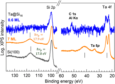 | ||
| Fig. 6 Wide-scan XPS spectra for the thin (0.6 ML) and thick (7 ML) films of the Ta@Si16 SA on C60. In the thick film, satellite peaks are observed at the higher energy sides of the main Si 2p and Ta 4f peaks, exhibiting a common energy separation of 17.9 eV. These satellite peaks originate from the energy loss of photoelectrons due to plasmonic excitation in the Ta@Si16 film. The plasma frequency (hνp) is slightly higher than that observed for a clean Si(100) single crystal (hνp = 17.0 eV, bottom spectrum).76 | ||
The energy of plasmon energy loss, hνp = 17.9 eV, is slightly higher than that of bulk Si (hνp = 17.0 eV, see the bottom in Fig. 6).76 It is known that the hνp changes with doping and quantum confinement, as reported in the literature when observing with XPS or electron energy loss spectroscopy (EELS) in Si-based systems.77–81 In single Si nanocrystals with >2 nm diameter prepared from silane gas plasma,77 the quantum confinement effect generally induces a blue shift of hνp (∼1 eV in the smallest nanocrystals) because of the enlargement of the band gap. However, the quantum confinement effect can be excluded in the present system of the thick SA film, as no plasmon-induced energy loss peak is observable in the thin film (0.6 ML); the individual size of the Ta@Si16 SA is too small to have the plasma oscillations of their valence electrons. Therefore, the blue shift of the hνp in the Ta@Si16 film is considered to result from the effect of Ta doping in the Si cage (i.e. the doping effect81), although it is difficult to separately discuss the doping effects from many other possibilities (e.g. crystallinity, electronic structure, etc.). Note that a slight blue shift (0.3 eV) has been observed for multilayered Sin NCs on the substrate.79
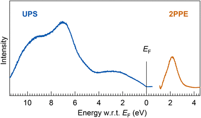 | ||
| Fig. 7 (bottom) UPS and 2PPE spectra of a thick Ta@Si16 SA film (7 MLs). The energy onset at EF in the UPS spectrum indicates the ohmic electronic conduction of the Ta@Si16 SA film. The broad valence and conduction band features, EF − 2.6 eV, −7.0 eV, and −9.6 eV in UPS and EF + 2.1 eV in 2PPE, are observed. The experimental results are compared with DFT calculations for the geometric isomer of neutral species and cations, as shown ESI Fig. S8.† | ||
The electronic structures in the UPS spectrum exhibit broad features, implying a few major components such as those at binding energies of EF − 2.6, −7.0, and −9.6 eV, while the conduction band feature is also resolved at EF + 2.1 eV, as shown in Fig. 2(a). These broad electronic features might be due to inter-SA interactions between the non-ligated Si caged SAs, providing the plasmon-loss peaks in the XPS spectrum, as shown in Fig. 6. Note that we carefully evaluated the electronic states of the Ta@Si16 SA film using UPS (and 2PPE) that are generally sensitive to oxidation or degradation of the topmost surface. Indeed, as evidenced by the drastic change in the UPS spectrum when the SA film is exposed to oxygen molecules (see ESI Fig. S3†), the resulting UPS spectrum closely resembles that of a thermally oxidized Si substrate.82
Importantly, the electronic structures are composed of more than 20 electronic states rather than a few broadened electronic states; the electronic states for a few geometric isomers of the free Ta@Si16 neutral species and cations are calculated through DFT calculations (see ESI Note S2†). The comparison between the experimental and theoretical results is shown in ESI Fig. S8.† Although it is not straightforward to correlate the electronic structures in the assembled layers with the electronic states of isolated species obtained from the Kohn–Sham orbitals and eigenvalues from the DFT calculations,83,84 the calculations suggest that more than 20 electronic states are involved in the region. The calculated electronic states for a few geometric isomers are shown in ESI Fig. S9 and Tables S1 (cation) and S2 (neutral).† While the Kohn–Sham orbitals and orbital energies cannot exactly reproduce the electronic transitions, the comparison gives a rough picture of the electronic structures, breaking down the broadened electronic features in the condensed phase through inter-SA interactions. This also serves as a good target for extensive calculations of the electronic states using Hartree–Fock-based calculations.
4. Conclusions
To conclude, we have precisely fabricated a Ta@Si16 SA film with mass-selective deposition onto a C60 substrate. The work function decreases at the initial deposition of the SA (<1 ML) due to the formation of a dipole moment at the SA–substrate interface. Under the irradiation of a femtosecond laser, the photoemission is drastically enhanced because of the distinct nonlinear optical responses of Ta@Si16 SAs, where the intense photoemission signal enables the visualization of the interfacial near-field due to plasmonic excitation. From XPS analysis, the charge state of the Ta@Si16 SA in the thick film is characterized as Ta+@(Si16)−, making neutral the Ta@Si16 SAs as a whole. The UPS/2PPE spectra show the valence and conduction electronic structures of Ta@Si16 SA films revealing broadening effects due to inter-SA interactions. The valence and conduction band features are in agreement with DFT calculations, originating from the superatomic nature. The electronic and optical characterization studies of the well-controlled SA films will facilitate the emergence of an era utilizing the novel functionalities of SA-assembled systems.Author contributions
MS, TO, and TK conducted the photoelectron spectroscopy measurements of the SA films. MS and KY acquired the 2P-PEEM images of the SA-decorated plasmonic sample. HT, TI, and TM calculated the electronic structures of the SAs. MS and AN contributed to the writing processes. AN supervised the overall project.Data availability
The data supporting this article have been included as part of the ESI.†Conflicts of interest
There are no conflicts to declare.Acknowledgements
This work was partly supported by the program of Exploratory Research for Advanced Technology (ERATO) in the Japan Science and Technology Agency (JST) entitled the “Nakajima Designer Nanocluster Assembly Project”, JSPS KAKENHI of Grant-in-Aid for Scientific Research (A) No. 19H00890, Scientific Research (B) No. 23H01939, 24K01277, and 24K01442 and Scientific Research (C) No. 18K04942, and Transformative Research Areas (A) “Hyper–Ordered Structures Science” No. 21H05573. A. N. is grateful for support from the Alexander von Humboldt Foundation.References
- T. Bernhardt, U. Heiz and U. Landman, Chemical and Catalytic Properties of Size-Selected Free and Supported Clusters, Springer, Berlin, Heidelberg, 2007 Search PubMed.
- A. W. Castleman Jr., J. Phys. Chem. Lett., 2011, 2, 1062–1069 CrossRef.
- P. Jena, J. Phys. Chem. Lett., 2013, 4, 1432–1442 CrossRef CAS PubMed.
- D. A. Tomalia and S. N. Khanna, Chem. Rev., 2016, 116, 2705–2774 CrossRef CAS PubMed.
- Z. Luo, A. W. Castleman Jr. and S. N. Khanna, Chem. Rev., 2016, 116, 14456–14492 CrossRef CAS PubMed.
- A. C. Reber and S. N. Khanna, Acc. Chem. Res., 2017, 50, 255–263 CrossRef CAS PubMed.
- P. Jena and Q. Sun, Chem. Rev., 2018, 118, 5755–5870 CrossRef CAS PubMed.
- P. Ferrari, J. Vanbuel, E. Janssens and P. Lievens, Acc. Chem. Res., 2018, 51, 3174–3182 CrossRef CAS PubMed.
- H. W. Kroto, J. R. Heath, S. C. O'Brien, R. F. Curl and R. E. Smalley, Nature, 1985, 318, 162–163 CrossRef CAS.
- D. E. Bergeron, A. W. Castleman Jr., T. Morisato and S. N. Khanna, Science, 2004, 304, 84–87 CrossRef CAS PubMed.
- J. U. Reveles, S. N. Khanna, P. J. Roach and A. W. Castleman Jr., Proc. Natl. Acad. Sci. U. S. A., 2006, 103, 18405–18410 CrossRef CAS PubMed.
- A. C. Reber, S. N. Khanna and A. W. Castleman Jr., J. Am. Chem. Soc., 2007, 129, 10189–10194 CrossRef CAS PubMed.
- A. Nakajima, T. Kishi, T. Sugioka and K. Kaya, Chem. Phys. Lett., 1991, 187, 239–244 CrossRef.
- K. Koyasu, M. Akutsu, M. Mitsui and A. Nakajima, J. Am. Chem. Soc., 2005, 127, 4998–4999 CrossRef CAS PubMed.
- H. Hiura, T. Miyazaki and T. Kanayama, Phys. Rev. Lett., 2001, 86, 1733–1736 CrossRef CAS PubMed.
- M. B. Torres, E. M. Fernández and L. C. Balbás, Phys. Rev. B: Condens. Matter Mater. Phys., 2007, 75, 205425 CrossRef.
- K. Koyasu, J. Atobe, M. Akutsu, M. Mitsui and A. Nakajima, J. Phys. Chem. A, 2007, 111, 42–49 CrossRef CAS PubMed.
- J. T. Lau, K. Hirsch, Ph. Klar, A. Langenberg, F. Lonfink, R. Richter, J. Rittman, M. Vogel, V. Zamudio-Bayer, T. Möller and B. von Issendorff, Phys. Rev. A, 2009, 79, 053201 CrossRef.
- J. T. Lau, M. Vogel, A. Langenberg, K. Hirsch, J. Rittmann, V. Zamudio-Bayer, T. Möller and B. von Issendorff, J. Chem. Phys., 2011, 134, 041102 CrossRef CAS PubMed.
- J. Atobe, K. Koyasu, S. Furuse and A. Nakajima, Phys. Chem. Chem. Phys., 2012, 14, 9403–9410 RSC.
- A. Sen and S. Sen, J. Phys. Chem. C, 2017, 121, 28490–28497 CrossRef CAS.
- Y. Negishi, K. Nobusada and T. Tsukuda, J. Am. Chem. Soc., 2005, 127, 5261–5270 CrossRef CAS PubMed.
- Y. Negishi, H. Tsunoyama, M. Suzuki, N. Kawamura, M. M. Matsushita, K. Maruyama, T. Sugawara, T. Yokoyama and T. Tsukuda, J. Am. Chem. Soc., 2006, 128, 12034–12035 CrossRef CAS PubMed.
- H. Häkkinen, Chem. Soc. Rev., 2008, 37, 1847–1859 RSC.
- T. Laaksonen, V. Ruiz, P. Liljeroth and B. M. Quinn, Chem. Soc. Rev., 2008, 37, 1836–1846 RSC.
- R. Jin, Nanoscale, 2010, 2, 343–362 RSC.
- M. Shibuta, T. Ohta, M. Nakaya, H. Tsunoyama, T. Eguchi and A. Nakajima, J. Am. Chem. Soc., 2015, 137, 14015–14018 CrossRef CAS PubMed.
- T. Ohta, M. Shibuta, H. Tsunoyama, T. Eguchi and A. Nakajima, J. Phys. Chem. C, 2016, 120, 15265–15271 CrossRef CAS.
- H. Tsunoyama, H. Akatsuka, M. Shibuta, T. Iwasa, Y. Mizuhata, N. Tokitoh and A. Nakajima, J. Phys. Chem. C, 2017, 121, 20507–20516 CrossRef CAS.
- H. Tsunoyama, M. Shibuta, M. Nakaya, T. Eguchi and A. Nakajima, Acc. Chem. Res., 2018, 51, 1735–1745 CrossRef CAS PubMed.
- M. Shibuta, T. Kamoshida, T. Ohta, H. Tsunoyama and A. Nakajima, Commun. Chem., 2018, 1, 50 CrossRef.
- M. Shibuta, T. Niikura, T. Kamoshida, H. Tsunoyama and A. Nakajima, Phys. Chem. Chem. Phys., 2018, 20, 26273–26279 RSC.
- T. Kamoshida, M. Shibuta, T. Ohta, T. Eguchi and A. Nakajima, J. Phys. Chem. C, 2022, 126, 10889–10899 CrossRef CAS.
- M. Shibuta, T. Inoue, T. Kamoshida, T. Eguchi and A. Nakajima, Nat. Commun., 2022, 13, 1336 CrossRef CAS PubMed.
- T. Inoue, M. Hatanaka and A. Nakajima, J. Am. Chem. Soc., 2023, 145, 23088 CrossRef CAS PubMed.
- K. Terasaka, T. Kamoshida, T. Ichikawa, T. Yokoyama, M. Shibuta and A. Nakajima, J. Am. Chem. Soc., 2024, 146, 9605–9613 CrossRef CAS PubMed.
- S. N. Khanna and P. Jena, Phys. Rev. Lett., 1992, 69, 1664–1667 CrossRef CAS PubMed.
- S. N. Khanna and P. Jena, Phys. Rev. B: Condens. Matter Mater. Phys., 1995, 51, 13705–13716 CrossRef CAS PubMed.
- M. Nakaya, T. Iwasa, H. Tsunoyama, T. Eguchi and A. Nakajima, Nanoscale, 2014, 6, 14702–14707 RSC.
- M. Nakaya, T. Iwasa, H. Tsunoyama, T. Eguchi and A. Nakajima, J. Phys. Chem. C, 2015, 119, 10962–10968 CrossRef CAS.
- T. Inoue, T. Ina, H. Masai, N. Kondo, F. Matsui, T. Kinoshita and A. Nakajima, J. Phys. Chem. Lett., 2024, 15, 5376–5381 CrossRef CAS PubMed.
- M. Shibuta, R. Takano and A. Nakajima, J. Phys. Chem. C, 2020, 124, 28108–28115 CrossRef CAS.
- T. Yokoyama, T. Chiba, N. Hirata, M. Shibuta and A. Nakajima, J. Phys. Chem. C, 2021, 125, 18420–18428 CrossRef CAS.
- T. Yokoyama and A. Nakajima, Phys. Chem. Chem. Phys., 2023, 25, 9738–9752 RSC.
- H. Petek and S. Ogawa, Prog. Surf. Sci., 1997, 56, 239–310 CrossRef CAS.
- J. Güdde and U. Höfer, Prog. Surf. Sci., 2005, 80, 49–91 CrossRef.
- T. Yamada and T. Munakata, Prog. Surf. Sci., 2018, 93, 108–130 CrossRef CAS.
- M. Shibuta and A. Nakajima, J. Phys. Chem. Lett., 2023, 14, 3285–3295 CrossRef CAS PubMed.
- M. Bauer, A. Marienfeld and M. Aeschlimann, Prog. Surf. Sci., 2015, 90, 319–376 CrossRef CAS.
- C. H. Zhang, H. Tsunoyama, H. Akatsuka, H. Sekiya, T. Nagase and A. Nakajima, J. Phys. Chem. A, 2013, 117, 10211–10217 CrossRef CAS PubMed.
- M. Aeschlimann, T. Brixner, A. Fischer, C. Kramer, P. Melchior, W. Pfeiffer, C. Schneider, C. Strüber, P. Tuchscherer and D. V. Voronine, Science, 2011, 333, 1723–1726 CrossRef CAS PubMed.
- C. Lemke, T. Leißner, A. Evlyukhin, J. W. Radke, A. Klick, J. Fiutowski, J. Kjelstrup-Hansen, H.-G. Rubahn, B. N. Chichkov, C. Reinhardt and M. Bauer, Nano Lett., 2014, 14, 2431–2435 CrossRef CAS PubMed.
- C. Lemke, T. Leißner, A. Klick, J. Fiutowski, J. W. Radke, M. Thomaschewski, J. Kjelstrup-Hansen, H.-G. Rubahn and M. Bauer, Appl. Phys. B: Lasers Opt., 2014, 116, 585–591 CrossRef CAS.
- K. Yamagiwa, M. Shibuta and A. Nakajima, Phys. Chem. Chem. Phys., 2017, 19, 13455–13461 RSC.
- K. Yamagiwa, M. Shibuta and A. Nakajima, ACS Nano, 2020, 14, 2044–2052 CrossRef CAS PubMed.
- M. D
![[a with combining cedilla]](https://www.rsc.org/images/entities/char_0061_0327.gif) browski, Y. Dai and H. Petek, Chem. Rev., 2020, 120, 6247–6287 CrossRef PubMed.
browski, Y. Dai and H. Petek, Chem. Rev., 2020, 120, 6247–6287 CrossRef PubMed. - M. Großmann, M. Black, J. Jaruschewski, A. Klick, T. Leißner, J. Fiutowski, H.-G. Rubahn and M. Bauer, Plasmonics, 2021, 16, 737–746 CrossRef.
- M. Hartelt, P. N. Terekhin, T. Eul, A.-K. Mahro, B. Frisch, E. Prinz, B. Rethfeld, B. Stadtmüller and M. Aeschlimann, ACS Nano, 2021, 15, 19559–19569 CrossRef CAS PubMed.
- T. Ohta, M. Shibuta, H. Tsunoyama, Y. Negishi, T. Eguchi and A. Nakajima, J. Phys. Chem. C, 2013, 117, 3674–3679 CrossRef CAS.
- M. Shibuta, K. Yamamoto, T. Ohta, T. Inoue, K. Mizoguchi, M. Nakaya, T. Eguchi and A. Nakajima, ACS Nano, 2021, 15, 1199–1209 CrossRef CAS PubMed.
- M. Shibuta, K. Yamamoto, T. Ohta, M. Nakaya, T. Eguchi and A. Nakajima, Sci. Rep., 2016, 6, 35853 CrossRef CAS PubMed.
- M. Shibuta, N. Hirata, T. Eguchi and A. Nakajima, ACS Nano, 2017, 11, 4307–4314 CrossRef CAS PubMed.
- M. Shibuta, K. Yamagiwa, T. Eguchi and A. Nakajima, Appl. Phys. Lett., 2016, 109, 203111 CrossRef.
- M. Shibuta and A. Nakajima, Nanoscale, 2024, 16, 12397–12405 RSC.
- D. L. Huang, P. D. Dau, H. T. Liu and L. S. Wang, J. Chem. Phys., 2014, 140, 224315 CrossRef PubMed.
- H. Lüth, Solid Surfaces, Interfaces and Thin Films, Springer, Berlin, 2001 Search PubMed.
- M. Jung, D. Shin, S.-D. Sohn, S.-Y. Kwon, N. Park and H.-J. Shin, Nanoscale, 2014, 6, 11835 RSC.
- T. Iwasa and A. Nakajima, J. Phys. Chem. C, 2012, 116, 14071–14077 CrossRef CAS.
- M. Chen, I. P. Batra and C. R. Brundle, J. Vac. Sci. Technol., 1979, 16, 1216–1220 CrossRef CAS.
- J. C. Green and P. Decleva, Coord. Chem. Rev., 2005, 249, 209–228 CrossRef CAS.
- A. Kubo, N. Pontius and H. Petek, Nano Lett., 2007, 7, 470–475 CrossRef CAS PubMed.
- M. Shibuta, T. Eguchi and A. Nakajima, Plasmonics, 2013, 8, 1411–1415 CrossRef CAS.
- E. Kretschmann, Z. Phys., 1971, 241, 313–324 CrossRef CAS.
- S. L. Ren, Y. Wang, A. M. Rao, E. McRae, J. M. Holden, T. Hager, K. Wang, W.-T. Lee, H. F. Ni, J. Selegue and P. C. Eklund, Appl. Phys. Lett., 1991, 59, 2678–2680 CrossRef CAS.
- W. Krätschmer, L. D. Lamb, K. Fostiropoulos and D. R. Huffman, Nature, 1990, 347, 354–358 CrossRef.
- T. L. Barr, Modern ESCA, The Principles and Practice of X-Ray Photo-electron Spectroscopy, CRC, Boca Raton, 1994 Search PubMed.
- M. Mitome, Y. Yamazaki, H. Takagi and T. Nakagiri, J. Appl. Phys., 1992, 72, 812–814 CrossRef CAS.
- N. Dibiase, G. Gabetta, A. Lumachi, M. Scagliotti and F. Parmigiani, Appl. Phys. Lett., 1995, 67, 2491–2493 CrossRef CAS.
- P. Mélinon, P. Kéghélian, B. Prével, A. Perez, G. Guiraud, J. LeBrusq, J. Lermé, M. Pellarin and M. Broyer, J. Chem. Phys., 1997, 107, 10278–10287 CrossRef.
- N. Mannella, G. Gabetta and F. Parmigiani, Appl. Phys. Lett., 2001, 79, 4432–4434 CrossRef CAS.
- M. Duchamp, C. B. Boothroyd, M. S. Moreno, B. B. van Aken, W. J. Soppe and R. E. Dunin-Borkowski, J. Appl. Phys., 2013, 113, 093513 CrossRef.
- A. J. Schell-Sorokin and J. E. Demuth, Surf. Sci., 1985, 157, 273–296 CrossRef CAS.
- R. Stowasser and R. Hoffmann, J. Am. Chem. Soc., 1999, 121, 3414–3420 CrossRef CAS.
- R. van Meer, O. V. Gritsenko and E. J. Baerends, J. Chem. Theory Comput., 2014, 10, 4432–4441 CrossRef CAS PubMed.
Footnotes |
| † Electronic supplementary information (ESI) available: Notes S1 and S2, Fig. S1–S9, and Tables S1 and S2. See DOI: https://doi.org/10.1039/d4nr02778g |
| ‡ Present address: Department of Physics and Electronics, Graduate School of Engineering, Osaka Metropolitan University, 1-1, Gakuen-cho, Naka-ku, Sakai, Osaka 599-8531, Japan. |
| This journal is © The Royal Society of Chemistry 2024 |

