
Minimizing defect states through multidentate coordination and morphology regulation for enhancing the performance of inverted perovskite solar cells†
Himangshu
Baishya
 a,
Mayur Jagdishbhai
Patel
b,
Ramkrishna
Das Adhikari
a,
Deepak
Yadav
b and
Parameswar Krishnan
Iyer
*ab
a,
Mayur Jagdishbhai
Patel
b,
Ramkrishna
Das Adhikari
a,
Deepak
Yadav
b and
Parameswar Krishnan
Iyer
*ab
aCentre for Nanotechnology, Indian Institute of Technology Guwahati, Guwahati 781039, Assam, India. E-mail: pki@iitg.ac.in
bDepartment of Chemistry, Indian Institute of Technology Guwahati, Guwahati 781039, Assam, India
First published on 25th October 2024
Abstract
The diversity of the defects present in perovskite materials negatively impacts both the power conversion efficiency (PCE) and the long-term stability of perovskite solar cells (PSCs). The chemical passivation of these defects has been addressed through a multifunctional molecule, 4-((trifluoromethyl)thio)benzoic acid, that contains the carbonyl (C![[double bond, length as m-dash]](https://www.rsc.org/images/entities/char_e001.gif) O) group, which exhibits a strong passivation effect by interacting with both the organic cation (FA+) and uncoordinated Pb2+ ionic defects while the sulfur (S) heteroatom passivates Pb2+ defects at the grain boundary and on the surfaces of the perovskite layer. Additionally, the CF3 group protects the perovskite film from ambient degradation as well as stabilizing the perovskite framework by forming hydrogen and coordination bonds with the FA+ cation and Pb2+ ions, respectively. The interaction between CO and Pb2+ forms a Lewis acid–base adduct that regulates grain growth during crystallization, enhancing the perovskite film's surface morphology as confirmed by SEM, AFM, and PL mapping. This reduces trap-assisted recombination of charged carriers, thereby enhancing their lifetime and transport, as observed from TRPL, KPFM, and c-AFM analyses. As a result of the combined effect of the additive molecule, the optimized device showed a marked improvement in efficiency rising from 16.54% in the pristine device to 20.87% with a reduction in hysteresis. Moreover, the optimized device shows enhancement of stability by retaining ∼86% normalized PCE after 40 days of storage under ambient conditions at 25 ± 3 °C and a relative humidity of ∼45–55%.
O) group, which exhibits a strong passivation effect by interacting with both the organic cation (FA+) and uncoordinated Pb2+ ionic defects while the sulfur (S) heteroatom passivates Pb2+ defects at the grain boundary and on the surfaces of the perovskite layer. Additionally, the CF3 group protects the perovskite film from ambient degradation as well as stabilizing the perovskite framework by forming hydrogen and coordination bonds with the FA+ cation and Pb2+ ions, respectively. The interaction between CO and Pb2+ forms a Lewis acid–base adduct that regulates grain growth during crystallization, enhancing the perovskite film's surface morphology as confirmed by SEM, AFM, and PL mapping. This reduces trap-assisted recombination of charged carriers, thereby enhancing their lifetime and transport, as observed from TRPL, KPFM, and c-AFM analyses. As a result of the combined effect of the additive molecule, the optimized device showed a marked improvement in efficiency rising from 16.54% in the pristine device to 20.87% with a reduction in hysteresis. Moreover, the optimized device shows enhancement of stability by retaining ∼86% normalized PCE after 40 days of storage under ambient conditions at 25 ± 3 °C and a relative humidity of ∼45–55%.
1. Introduction
Organic–inorganic halide-based perovskite (OIHP) materials are advancing at a remarkable pace as promising photo-absorbing materials for next-generation photovoltaic technology, owing to their outstanding optoelectronic properties.1,2 These include a high optical absorption coefficient (∼105 cm−1), low exciton binding energy (∼30 meV), long carrier diffusion length (>1 μm), high defect tolerance, a tunable bandgap, low cost and low-temperature solution-processability.3–8 The utilization of MAPbI3 and MAPbBr3 OIHP materials in 2009 by Miyasaka et al., initially as organic dyes in dye-sensitized solar cells, marked a significant milestone. Since then, with substantial advancements in material engineering and device architecture optimization, the PCE of PSCs has soared from 3.8% in 2009 to 26.1% in 2023, rivaling established photovoltaic technologies.9,10 However, despite these strides in perovskite materials, stability issues in PSCs persist due to both intrinsic and extrinsic instability factors.11,12 The most efficient PSCs (PCE > 25%) utilize formamidinium lead triiodide (FAPbI3) as the perovskite active layer. While FA-based perovskites offer an optimum bandgap and superior thermal stability compared to methylammonium (MA)-based perovskites, they are prone to spontaneous phase transitions from the photo-active perovskite (α-black) phase to the non-photo-active perovskite (δ-yellow) phase at room temperature due to the mismatch in ionic size between formamidine (FA+) and the lead iodine octahedron [PbI6]4−.13,14 To address this challenge, replacing some FA+ cations with smaller ionic radius cations such as cesium or rubidium (Cs+, Rb+) to form a stable perovskite structure is emerging as an effective strategy. This substitution enhances the stability of the photoactive α-phase by adjusting the Goldschmidt's tolerance factor closer to the optimal range of “0.9–1” and enhancing the overall performance and reliability of PSCs.15–17The fabrication process of the perovskite absorber layer primarily utilizes solution-processable low-temperature methods leading to the formation of a polycrystalline structure with inherent grain boundaries (GBs).18,19 The morphology of the photoactive perovskite layer plays a pivotal role in determining both the open circuit voltage (VOC) and the fill factor (FF), where the surface morphology refers to the homogeneity of the film having uniform coverage, grain size, distribution, and texture, with an absence of pinholes. The rapid crystal growth process, particularly at elevated temperatures, introduces a wide range of defects, especially at GBs, and the surface of the perovskite layer is heavily dependent on the precursor composition and fabrication processes.20–22 These defects are categorized as shallow-level and deep-level defects, situated throughout the bulk and surface of the perovskites. Shallow-level defects, owing to their low formation energy, exhibit high densities at the band edge that decrease charge recombination rates, making perovskites highly defect tolerant. However, deep-level defects, such as uncoordinated Pb2+, metallic lead (Pb0), and PbI antisite, are easily formed after the organic volatile components escape during the thermal annealing process. This leaves behind uncoordinated Pb2+ and it may even be reduced to Pb0 during film preparation or device operation. These defects serve as primary sources of non-radiative recombination centers, ultimately leading to the annihilation of opposite charge carriers. Unlike shallow-level defects which have lower charge recombination rates, deep-level defects impede carrier escape due to their deep energy levels, resulting in a severe deficit in VOC in PSCs.23–25 In addition, defects and GBs act as migration paths for uncoordinated ions existing in the perovskite system during operation, resulting in serious hysteresis effects on PSCs and accelerating the degradation process by facilitating decomposition reactions at interfaces.26–29 Consequently, the presence of defects in the perovskite significantly diminishes key photovoltaic parameters, particularly VOC and FF, thereby decreasing its overall PCE and hampering its long-term stability. Thus, fabricating high-quality perovskite films with homogeneous surface morphology featuring large grains, fewer GBs, and full coverage with smooth top surfaces is crucial to improving light-harvesting efficiency and reducing undesirable shunt losses by mitigating defects to achieve high performance and stable PSCs.
Numerous efforts have been dedicated to enhancing the crystalline quality and surface morphology of perovskite films, aiming to improve charge transport and collection. This pursuit has led to a diverse array of techniques including compositional, solvent, additive, interface, and dimensional engineering.30–33 Among these strategies, additive engineering stands out as a simple yet effective approach for mitigating defect states, suppressing ion migration at GBs, and protecting the perovskite layer from moisture and oxygen through kinetic control of crystallization by introducing organic small molecules, polymers, inorganic salts, etc., into the perovskite precursor. Organic small molecules have garnered significant attention due to their tunable molecular structure and multifunctionality. These molecules possessing electron-donating and -accepting heteroatoms (S, N, O, P, etc.) and various functional groups such as carbonyl (CO), amine (–NH2), hydroxyl (–OH), and halide (–X) serve as effective defect passivators. Additionally, they modulate the morphology of the perovskite absorber layer through chemical interactions with the perovskite structure, thereby enhancing its optical and electronic properties.34–38 CO and SH are among the most frequently used functional groups, known for their passivation effect through coordinated bonding with uncoordinated Pb2+ ions. These groups exhibit significant potential in passivating under-coordinated Pb2+, PbI antisite, and Pb clusters.39–42 In addition, the commonly utilized CF3 serves as a multifunctional passivator that coordinates with Pb2+ ions and FA+/MA+ defects, forming ionic and hydrogen bonds, respectively. This coordination effectively immobilizes the cationic defect that stabilizes the perovskite composition while also leveraging its hydrophobic nature to protect the perovskite layer from moisture.43–45 Consequently, chemical passivation focuses on the mitigation of charge defects within the perovskite bulk and surface alongside regulating the surface of the perovskite film to enhance its overall performance.
In this study, we introduce a small organic additive molecule 4-((trifluoromethyl)thio)benzoic acid referred to as 4-TFTBA, as a multifunctional passivator into the Cs0.1FA0.9PbI3 perovskite precursor. Firstly, the carbonyl (CO) group in 4-TFTBA plays a crucial role in passivation, forming strong interactions with both organic cations (FA+) and uncoordinated Pb2+ ionic defects. Next, the sulfur (S) heteroatom effectively passivates Pb defects. Additionally, the hydrophobic nature of the CF3 group not only protects the perovskite film from ambient degradation but also stabilizes the perovskite structure by forming hydrogen and coordination bonds with the FA+ cation and Pb2+ ionic defects, respectively. Furthermore, the multifunctional additive molecule enhances the crystallization process and regulates the surface of the perovskite film, as confirmed through scanning electron microscopy (SEM) and atomic force microscopy (AFM) analyses. This results in a decrease in non-radiative recombination centers, ultimately improving the lifetime of charge carriers and facilitating their transport. These improvements are evident from analyses such as time-resolved photoluminescence (TRPL), conducting atomic force microscopy (c-AFM), and Kelvin probe force microscopy (KPFM). Consequently, the optimized device exhibited enormous improvement in both Voc and FF. As a result, the PSC device achieved its highest PCE increasing from 16.54% to 20.87% when using a 1 mg mL−1 concentration of 4-TFTBA. Furthermore, the unencapsulated optimized device displayed a retained normalized PCE of 86% compared to that of the pristine device (63%) after 40 days of storage under ambient atmospheric conditions at 25 ± 3 °C and a relative humidity of approximately 45–55%, indicating enhancement of the device stability.
2. Results and discussion
Fig. 1 illustrates the schematic representation of the interaction of additive molecules via different chemical bonds with the perovskite framework to passivate uncoordinated Pb2+, FA+, PbI antisite, Pb cluster, and I vacancy defects. Fourier transform infrared spectroscopy (FTIR) was systematically investigated to gain insight into the passivation effect of the functional groups of 4-TFTBA after interaction with different components of the perovskite precursor (Fig. S1†). Fig. 2a shows the typical stretching vibrational peak of the CO group of 4-TFTBA. After incorporation of FAI and PbI2 stock solution prepared in anhydrous DMSO solvent into 4-TFTBA powder, the CO peak shifted from 1691 cm−1 to 1695 and 1705 cm−1, respectively. This shift of the CO stretching vibrational peak indicates interaction with the cationic FA+ and Pb2+, which is further confirmed by the observed peak shift in liquid state 1H NMR (Fig. S2†).46 The larger peak shift for the interaction between CO and PbI2 confirms that under-coordinated Pb2+ defects bind more strongly with CO than FA+. This interaction forms a Lewis acid–base adduct due to electron delocalization that regulates the grain growth process during the crystallization of the perovskite film.39,47
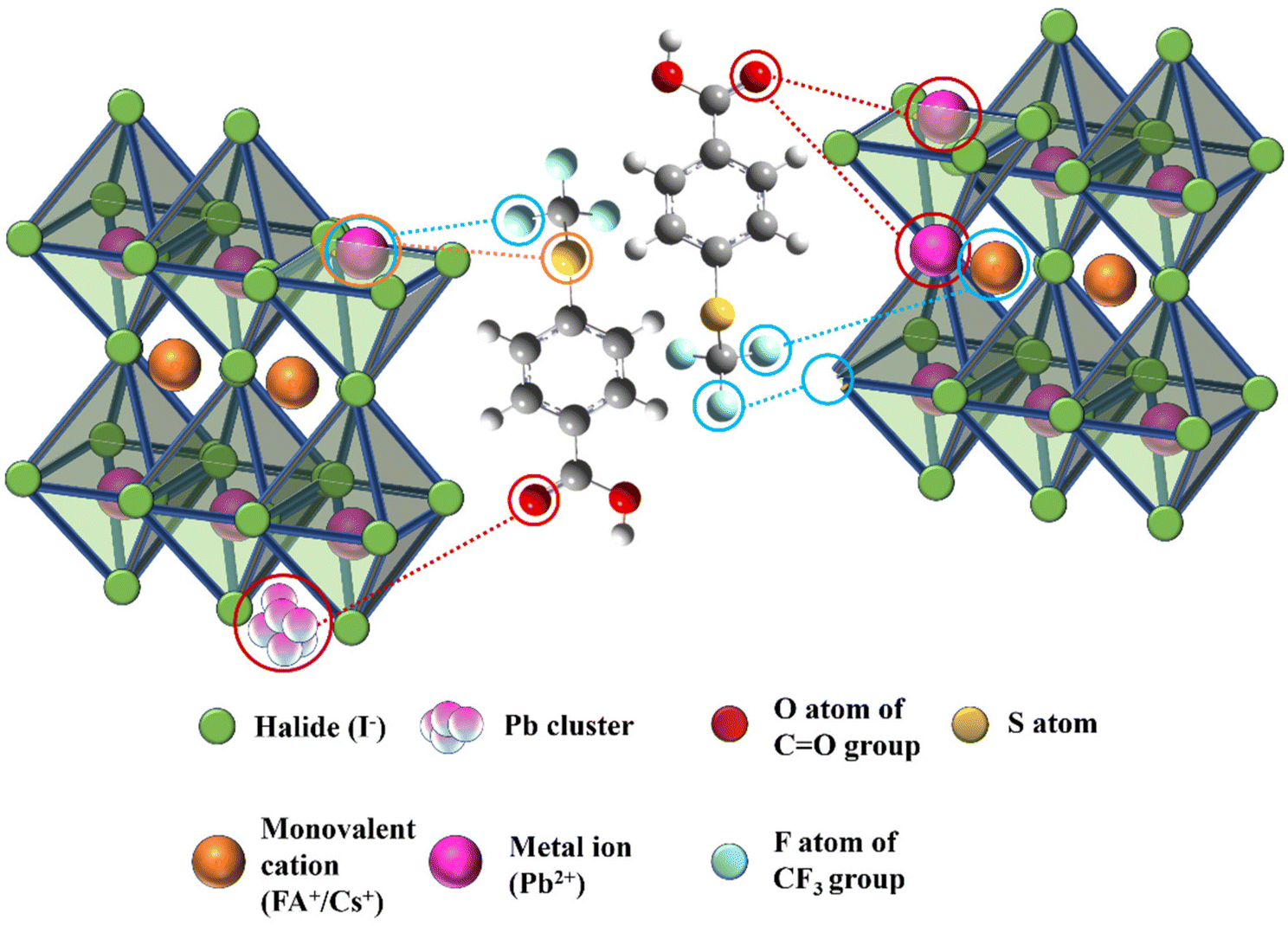 | ||
| Fig. 1 Schematic representation of the interaction between the 4-TFTBA additive molecule and the defect sites of the perovskite framework. | ||
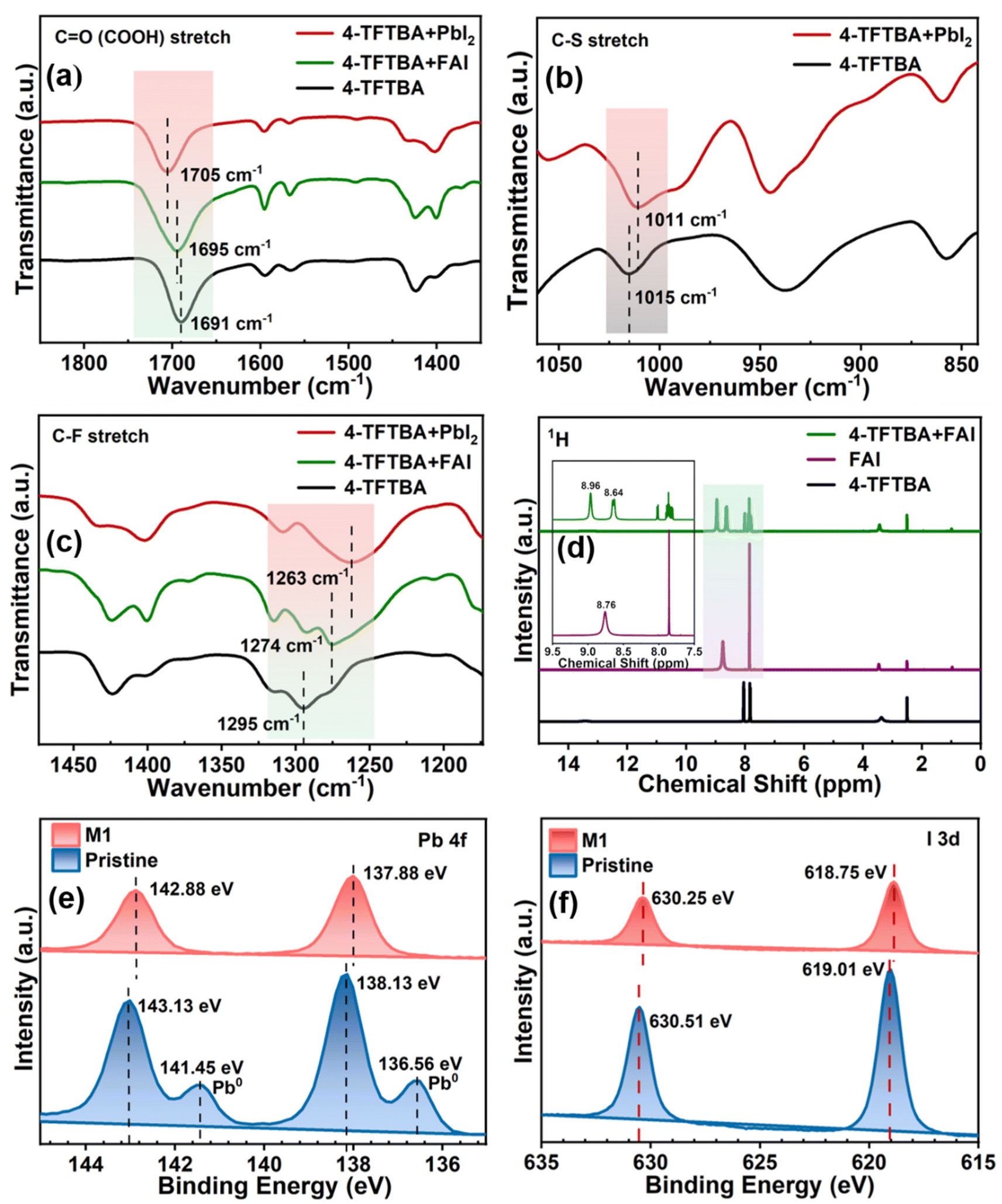 | ||
| Fig. 2 FTIR spectra of (a) CO, (b) C–S, and (c) C–F stretching vibration of 4-TFTBA with FAI and PbI2 precursors; (d) 1H NMR spectra of 4-TFTBA and 4-TFTBA + FAI; and XPS spectra of (e) Pb 4f and (f) I 3d orbital of the perovskite with and without modification by 4-TFTBA. | ||
Moreover, in Fig. 2b, the shift in the stretching vibrational peak of the C–S bond from 1015 to 1011 cm−1 after interaction with PbI2 due to sharing of the electron lone pair of S with Pb2+ further confirms the passivation of uncoordinated Pb2+ defects. Fig. 2c shows the shift of the typical stretching vibrational peak of the C–F bond from 1295 cm−1 to 1274 and 1263 cm−1 with the addition of FAI and PbI2 stock solution, respectively. This interaction between C–F and FA+ is due to the formation of the N–H⋯F hydrogen bond and the reduction in the corresponding vibrational frequency is attributed to the delocalization of the N–H bond electronic cloud that weakens the N–H chemical bond energy. The existence of a hydrogen bond between the CF3 group and FA+ was confirmed by liquid-state 1H NMR. As shown in Fig. 2d, the resonance peak at 8.76 ppm is attributed to the protonated ammonium of FAI dissolved in DMSO-d6. After the addition of 4-TFTBA to FAI, this peak is split into two components at 8.64 and 8.96 ppm, as shown in the magnified image, due to the two different chemical environments of FA+.48 This strong interaction between the CF3 group of the additive molecule and the FA+ cation inhibits the formation of FA vacancies.43,49 Furthermore, the interaction of the CF3 group with the perovskite components is verified by 19F NMR (Fig. S3†). The shift of the 19F peak of 4-TFTBA after treatment with FAI and PbI2 in DMSO-d6 indicates the formation of a hydrogen bond with FAI and a coordination bond with PbI2 where Pb–F leads to the passivation of iodine vacancies.50 These interactions play a beneficial role in anchoring the organic cation and Pb ions, thereby enhancing the stability of the perovskite structure.
X-ray photoelectron spectroscopy (XPS) analysis was conducted to examine the chemical environment of both the pristine and the optimized perovskite films (Fig. S4†). The pristine perovskite film exhibited two distinct peaks at 138.13 and 143.13 eV, as shown in Fig. 2e, corresponding to the Pb 4f7/2 and 4f5/2 orbitals, respectively. Upon the addition of 4-TFTBA, a slight downshift of both orbitals was observed. This shift in the Pb orbital energy is attributed to the possible bonding between 4-TFTBA and perovskite, consistent with the FTIR result where the electron cloud of CO increases the electron density at the uncoordinated Pb2+ and PbI defects on the perovskite surface, thereby preventing their reaction with moisture and oxygen.40,51 Additionally, the small hump observed in the pristine film related to metallic Pb clusters is generated due to iodine vacancies which hinder perovskite crystallization and lead to additional deep-defect levels. This results in increased non-radiative recombination and accelerates perovskite degradation.52 After modification, Pb clusters were effectively eliminated, as observed in Fig. 2e. Furthermore, Fig. 2f shows the I 3d orbital energy of the pristine perovskite film at 619.01 and 630.51 eV, which shifted to a lower binding energy after the incorporation of 4-TFTBA. This shift is attributed to the influence of the strong electronegative F atom on the electron cloud density of I, confirming the interaction with the Pb–I bond.48 These findings suggest that the 4-TFTBA additive molecule induces a multiple passivation effect on the perovskite film that effectively mitigates non-radiative charge recombination losses, which is beneficial for improving device performance.
The photophysical properties of all the perovskite films were examined through UV-vis absorption spectroscopy. As shown in Fig. 3a, it is evident that compared to the pristine perovskite film, all 4-TFTBA modified films denoted as M0.5, M1, and M1.5 having concentrations of 0.5, 1, and 1.5 mg mL−1, respectively, exhibited enhanced light absorption in the range of 450–550 nm. This enhancement is ascribed to the improved quality of the perovskite film after modification contributing to better light harvesting properties that increase the photocurrent in PSCs. The bandgap of both the pristine and the highest absorption modified perovskite film (M1 modified) was calculated from absorption data (Fig. S5†) using the Tauc plot and found to be 1.54 eV, suggesting no noticeable change in the bandgap after the incorporation of the additive molecule into the perovskite structure. The defect states in perovskite materials having low formation energy create energy levels at the band edges known as shallow-level defect states. These defects typically hinder the effective movement of charge carriers through trapping or de-trapping processes during collection.23 The influence of the additive molecule in passivating shallow-level defects was observed by calculating the Urbach energy (Eu) from the UV-vis profile. The Eu values (Fig. 3b) for pristine and M1 modified films were found to be 33.7 and 28.1 meV, respectively, indicating a reduction in the number of shallow-level defects, thereby enhancing the transport of photogenerated charge carriers which improves the VOC in PSC devices.53 To further investigate the effect of the additive molecule on the recombination process, we conducted steady-state photoluminescence (PL) measurements on both the pristine and all the additive-concentrated modified films fabricated on glass substrates. Fig. 3c demonstrates the highest enhancement of radiative recombination of photogenerated charge carriers in the M1 modified film when irradiated from the perovskite side indicating remarkable passivation of trap states existing at grain boundaries and the surface of the perovskite film. Additionally, the PL spectra of the M1-modified film exhibit a slight blue shift (∼3 nm) compared to the pristine film, indicating the passivation of shallow-level defects as observed in Urbach energy calculations. The crystallinity and phase of the perovskite film were assessed using X-ray diffraction (XRD). Both the perovskite films with and without modification exhibit signature Bragg peaks at 14.00°, 19.80°, 24.30°, 28.10°, 31.60°, 34.70°, 40.30°, and 42.86°, representing the (100), (110), (111), (200), (210), (211), (220), and (300) crystal planes, respectively (Fig. 3d). This confirms the formation of the photo-active α-phase, with no discernible change in the peak position after the incorporation of the additive, suggesting that the additive does not alter the perovskite structure.54 However, upon the addition of 4-TFTBA, the intensity of PbI2 at 12.7° decreases, confirming the conversion of most uncoordinated Pb2+ into the photo-active perovskite phase. Additionally, the increased intensity of crystal planes (100), (200), and (300) in the M1 modified film compared to the pristine film indicates an enhancement of the perovskite crystallinity. This enhancement was further confirmed by the decreased full-width at half maximum (FWHM) value in the modified film compared to the pristine film (Fig. S6†), which improves the charge transport in the perovskite film.
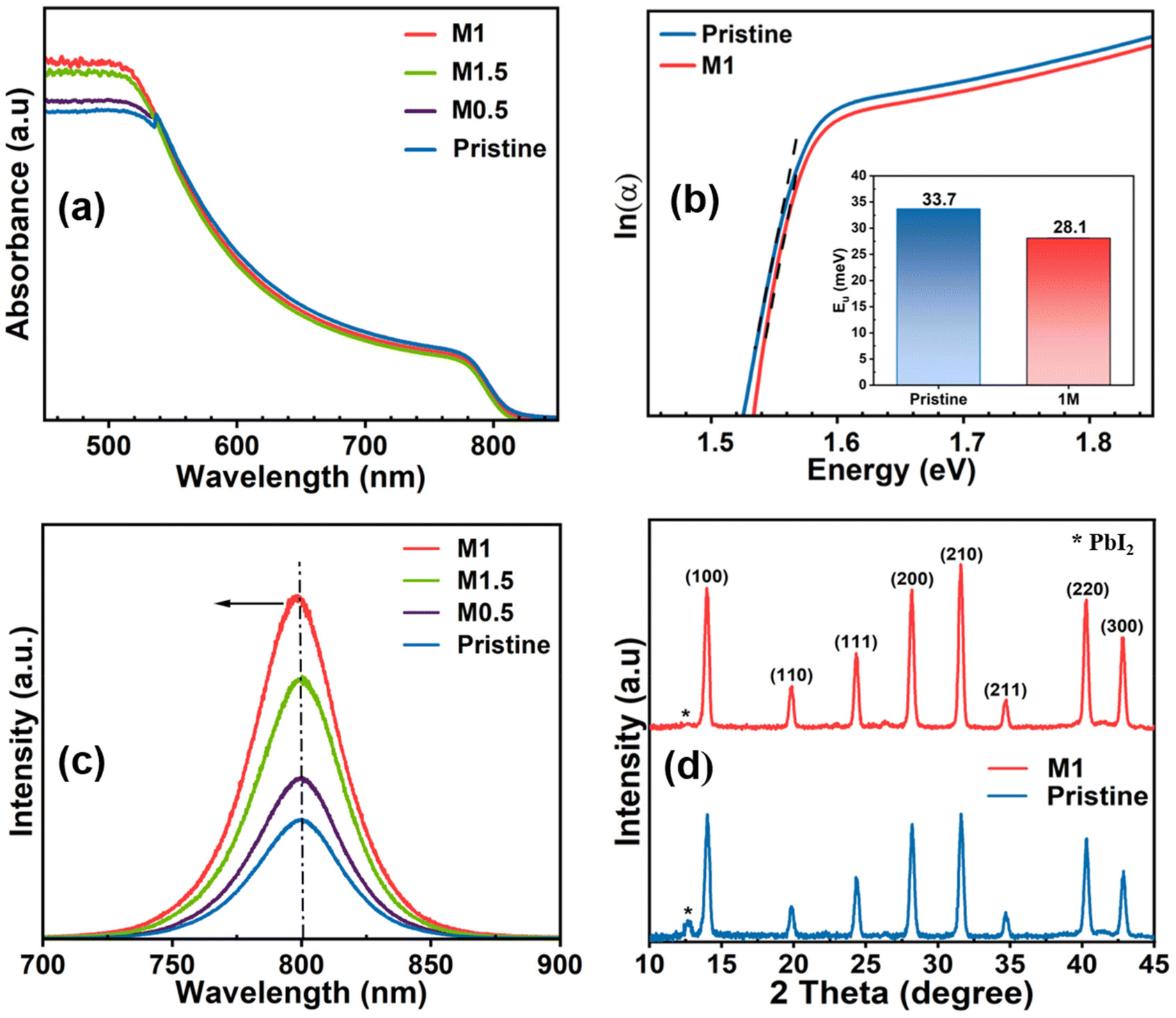 | ||
| Fig. 3 (a) Absorption profile of pristine and all modified perovskite films, (b) Urbach energy calculation of pristine and optimized films, (c) steady-state photoluminescence spectra of pristine and all modified films, and (d) XRD of pristine and optimized perovskite films. | ||
To assess the influence of the 4-TFTBA additive on the perovskite crystal growth and film morphology, SEM analysis was conducted. The SEM micrographs and the corresponding grain size distributions of pristine and M1-modified perovskite films are shown in Fig. 4a and b. It is apparent that the pristine film exhibits an average grain size of approximately 190 nm with numerous grain boundaries. In contrast, the M1-modified perovskite film demonstrates an improvement in the average grain size reaching approximately 290 nm along with a more homogeneous perovskite surface compared to the pristine film. This enhancement was further validated by cross-sectional SEM images fabricated in a stack of layers (FTO/NiOx/perovskite/PC61BM), as shown in Fig. 4c and d. Additionally, the M0.5 modified perovskite film displays a slight increase in the average grain size compared to the pristine film. However, the M1.5 modified perovskite film becomes overdosed with the additive molecule, resulting in interruptions in the perovskite growth and unfavorable grain formation (Fig. S7†). The enhancement in the grain size and the reduction of grain boundaries not only minimize non-radiative recombination centers but also contribute to a more compact film structure, as confirmed by cross-sectional SEM images. This compact morphology reduces the permeability of oxygen and moisture into the perovskite layer, thereby improving the environmental stability of the device. Additionally, the spatial distribution of the 4-TFTBA additive within the perovskite film, as revealed by time-of-flight secondary ion mass spectrometry (ToF-SIMS), demonstrates a gradient distribution from the surface to the bulk of the perovskite layer (Fig. S8†)). This gradient distribution effectively passivates defects at both the surface and grain boundaries, further enhancing the optoelectronic properties of the material.
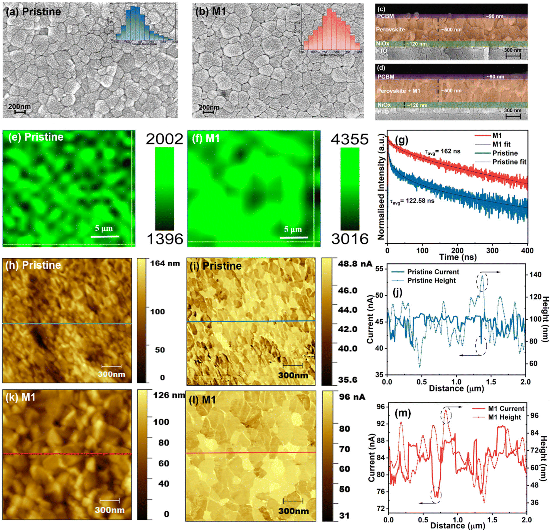 | ||
| Fig. 4 (a and b) Top view SEM micrograph, with inset showing grain size distribution, (c and d) cross-sectional SEM view, (e and f) PL mappings and (g) TRPL of pristine and optimized perovskite films; (h) height and (i) c-AFM current mapping images and (j) the corresponding line profile of the pristine perovskite film; and (k) height and (l) c-AFM current mapping images and (m) the corresponding line profile of the optimized film. | ||
Considering the critical role of perovskite film surface homogeneity in PSCs for efficient charge transport, PL mapping of a 20 × 20 μm2 area of both pristine and M1-modified perovskite films was conducted by irradiating the films coated on a glass substrate with a 532 nm laser source. As shown in Fig. 4e and f, it is obvious that the M1-modified film exhibits better spatial homogeneity on the surface where the intensity of radiative recombination of photogenerated charge carriers is enhanced, owing to the reduction of the number of traps at GBs and surfaces compared to the pristine film.55
Furthermore, TRPL of the pristine and M1-modified films was carried out to investigate the charge transfer dynamics. As illustrated in Fig. 4g, the corresponding TRPL decay curves were fitted with a biexponential decay equation (eqn (S1)†), and the corresponding fitting parameters are listed in Table S1.† The optimized perovskite film shows a prolonged τavg of 162 ns compared to 122.58 ns for the pristine perovskite film, indicating a slower recombination rate of charge carriers that enhances its transport and collection, which is attributed to the effective passivation of trap states of the perovskite film.56,57 AFM was employed to examine the smoothness of perovskite films with and without modification (Fig. S9†). The M1-modified perovskite film displays a smoother surface with the lowest root mean square (RMS) surface roughness value of approximately 14 nm, compared to the pristine film with an RMS value of around 22 nm. This smoother surface of the perovskite layer facilitates efficient charge transport by reducing charge trapping at the perovskite/ETL interface which improves the photovoltaic performance of PSCs. Furthermore, KPFM and c-AFM were conducted under ambient conditions on an FTO/NiOx/perovskite structure to observe changes in the electrical properties of the perovskite film after modification. As illustrated in Fig. S10,† there is a noticeable increase in the surface potential value of the M1-modified film compared to the pristine perovskite, which facilitates efficient charge separation due to enhancement of the grain size that reduces recombination loss.40 Additionally, Fig. 4h–m displays the morphology and current mapping images of the pristine and M1-modified films alongside the corresponding height and current line profiles. The c-AFM image of the M1-modified film exhibits a brighter and more homogeneous current profile compared to the pristine perovskite film, indicating an enhancement of conductivity, thereby facilitating improved charge transport. The line profiles derived from the morphology and current mapping images are presented in Fig. 4j and m. The current distribution of the M1-modified perovskite film shows a significant discrepancy between grains’ interior and GBs. The GBs exhibit a lower conductivity as compared to the grain interior after modification, indicating the effective passivation of trap states located at the GBs, which minimizes charge recombination and ion migration pathways in the perovskite film.58,59 These findings indicate that the optimized concentration of the 4-TFTBA additive not only improves the crystallization and regulates the morphology by manipulating grain growth processes but also enhances the lifetime of the charge carriers and the conductivity, which improves charge transport by reducing charge trapping at the perovskite film, thereby benefiting the overall device performance.
A series of p-i-n architecture PSC devices having the configuration FTO/NiOx/perovskite/PC61BM/rhodamine/Ag was fabricated (Fig. 5a) with and without additive modification of the perovskite layer to assess the effects of the additive molecule on the photovoltaic parameters. The current density–voltage (J–V) curves of the pristine, M0.5, M1, and M1.5 modified devices were measured under a simulated sunlight intensity of 100 mW cm−2, as depicted in Fig. 5b, and all the measured photovoltaic parameters are listed in Table 1.
 | ||
| Fig. 5 (a) Schematic diagram of inverted PSC, (b) J–V curve of pristine and all modified devices, (c) J–V curve of the pristine and optimized devices in forward and reverse scan, (d) EQE spectra and integrated JSC value of the pristine and optimized devices. | ||
| Device | Scan direction | J SC (mA cm−2) | V OC (mV) | FF (%) | PCE (%) | Average (PCE, %) | HI (%) |
|---|---|---|---|---|---|---|---|
| Pristine | FS | 22.56 | 1003.10 | 69.60 | 15.74 | 15.80 | 5.08 |
| RS | 22.47 | 1030.70 | 71.40 | 16.54 | |||
| M0.5 | FS | 22.91 | 1053.60 | 72.30 | 17.46 | 17.92 | 3.84 |
| RS | 23.46 | 1059.10 | 73.00 | 18.13 | |||
| M1 | FS | 24.49 | 1103.90 | 75.70 | 20.47 | 20.44 | 1.95 |
| RS | 24.74 | 1096.20 | 77.00 | 20.87 | |||
| M1.5 | FS | 23.58 | 1082.30 | 74.10 | 18.91 | 19.17 | 2.22 |
| RS | 24.13 | 1076.90 | 74.40 | 19.33 |
The pristine device exhibited the highest PCE of 16.54% at a scan rate of 10 mV s−1 along with a VOC of 1030.70 mV, a short-circuit current density (JSC) of 22.47 mA cm−2, and an FF of 71.40 (Fig. 5c). Upon addition of 0.5 mg mL−1 (0.5 M modified) of the additive molecule, all the photovoltaic parameters showed improvement and the highest PCE reached was 18.13%. Further increasing the concentration of the additive molecule to 1 mg mL−1 (M1 modified) resulted in an enormous improvement in all the photovoltaic parameters. The highest PCE reached 20.87% with a JSC of 24.74 mA cm−2, a VOC of 1096.20 mV, and an FF of 77.00%. The considerable enhancement in the VOC and FF could be attributed to the successful passivation of non-radiative recombination centers at GBs and the perovskite surface via strong interaction of multifunctional groups of the additive molecule with the perovskite framework as evident from FTIR, NMR, and XPS analyses. Additionally, the improvement in the JSC value in the M1-modified devices can be attributed to the enhanced light-harvesting properties and charge transport resulting from the improved surface morphology of the perovskite film. However, increasing the concentration of the additive molecule to 1.5 mg mL−1 (1.5 M modified) resulted in decreases in the device parameters, as listed in Table 1, which are directly associated with the decrease in the homogeneity of the perovskite film due to the overdose of additive concentration that led to interruption of the grain growth process as observed from SEM and AFM analyses. The hysteresis in PSCs mainly originates from bulk or surface defects that facilitate ion migration during the operation of PSCs. In Table 1, the hysteresis indexes (HI) of all the devices are compared using eqn (S2).† The pristine device shows an HI value of 5.08%, which is reduced to 1.95% in the M1-modified device. The reduction in the HI value in M1-modified devices could be attributed to the suppression of charge defects at the GBs and the surface of the perovskite layer that mitigate ion migration.
The reliability of the JSC value obtained from the J–V curve is verified by external quantum efficiency (EQE) measurements, as depicted in Fig. 5d. The M1-modified device exhibits an increased EQE response in the wavelength range of 400–700 nm compared to the pristine device. The enhanced incident photon-to-current efficiency (ICPE) in the modified device is attributed to the reduction of photogenerated charge recombination, which results from the passivation of defect states and the improved morphology of the modified perovskite film. The integrated JSC values calculated from the EQE data are 22.32 and 23.95 mA cm−2 for the pristine and optimized devices, respectively, consistent with the JSC value obtained from the J–V graph with a slight acceptable deviation. The steady-state current and PCE of the devices were also recorded at the maximum power point (MPP) to examine the photostability by continuous illumination for up to 300 s, as shown in Fig. 6a. It is obvious that the M1-modified device exhibits a more stabilized photocurrent and PCE compared to the pristine device. The reproducibility and reliability of the device performance were thoroughly analyzed by assessing a batch of 20 devices for both pristine and M1-modified perovskite films. The statistical distribution of all the photovoltaic parameters of these devices is illustrated in Fig. S11.† Notably, the M1-modified devices displayed a concentrated distribution of all photovoltaic parameters compared to pristine devices indicating superior reproducibility and reliability.
 | ||
| Fig. 6 (a) Stabilized photocurrent and PCE, (b) Mott–Schottky plot, (c) light intensity-dependent VOC, (d) Nyquist plot fitted with the respective equivalent circuit, (e) dark J–V plot, and (f) SCLC measurement of the hole-only-device of the pristine and optimized devices, respectively. | ||
The improvement in VOC in the optimized device is elucidated through capacitance–voltage (C–V) measurements under dark conditions, determining the built-in potential (Vbi) via the Mott–Schottky method (eqn (S3)†), as shown in Fig. 6b. The enhanced Vbi of 0.93 V in the optimized device compared to that of the pristine device (0.86 V) implies a strengthened driving force for the separation and collection of charge carriers attributable to the suppression of trap states in the perovskite film.60 Furthermore, the underlying recombination mechanism of charge carriers in PSCs was investigated by calculating the ideality factor (n) using eqn (S4)† based on the light intensity-dependent VOC. Fig. 6c presents the fitted data for the semi-log plot of the light intensity-dependent VOC for both pristine and optimized devices. The n value for the pristine device was found to be 1.74, which was reduced to 1.48 for the optimized device. The larger n value of the pristine device indicates a high influence of the non-radiative recombination due to the presence of a high level of trap density. However, the reduction in the n value towards unity in the optimized device suggests that trap-assisted recombination of charge carriers is profoundly suppressed, consequently improving the VOC and FF which enhances the overall device performance.61
Electrochemical impedance spectroscopy (EIS) measurements were conducted under dark conditions at the maximum power point voltage (Vmpp) for both the pristine and M1-modified devices to investigate the carrier transport process. The Nyquist plots were fitted accordingly by an equivalent circuit comprising a series resistance (RS) and charge recombination resistance (Rrec), as shown in Fig. 6d, with the corresponding fitting parameters summarized in Table S2†. The increased semi-circular arc in the M1-modified device indicates a considerably increased Rrec, consistent with facilitated charge transfer and reduced recombination.62 Consequently, the optimized device achieved higher VOC and FF values compared to pristine devices. Moreover, the dark J–V plot (Fig. 6e) exhibited a two-order-of-magnitude lower leakage current in the optimized device compared to the pristine device, indicating a smaller trap-assisted generation–recombination current facilitated by the reduced defect density. Additionally, the steep slope of the dark J–V curves for the M1-modified device in the high forward bias region indicates low series resistance and efficient charge transport.63 The trap density for the charge carriers in the devices was calculated using the space-charge limited current (SCLC) model by fabricating single carrier (hole only) devices having the architecture FTO/NiOx/perovskite/MoO3/Ag. The obtained results for the pristine and M1 modified devices are shown in Fig. 6f. The resulting plot shows three different regimes: ohmic, trap-filled limited, and trap-free SCLC regimes at low, intermediate, and high biases, respectively. The trap-filled limited voltage (VTFL) defined at the kink point between the ohmic and trap-filled regime reduces from 0.34 to 0.23 V in the M1-modified device. Furthermore, the trap density (ηtrap) in the perovskite film of both the pristine and modified devices was calculated using eqn (S5).† The trap density for the M1-modified device was found to be 3.56 × 1016 cm−3, which was lower than that of the pristine device 5.26 × 1016 cm−3, indicating successful passivation of trap states.
Aside from efficiency, the long-term stability of PSCs is a critical parameter for their commercialization. The degradation of PSCs can initiate from various factors, including oxidation of the top surface, ion mobilization at the perovskite interface, or intrinsic defects present in the perovskite layer leading to structural imperfections. Thus, the perovskite layer with homogeneous grain growth, fewer GBs, and a highly crystalline nature plays a pivotal role in degradation processes. Initially, the environmental stability of the perovskite films with and without additives was examined through XRD analysis (Fig. 7a and b) at specific time intervals by storing the films at a relative humidity (RH) of 45–55% and a temperature of 25 ± 3 °C. The pristine perovskite film exhibited a sharp PbI2 peak at 12.6° under fresh conditions which became more pronounced after 40 days along with the non-photo active perovskite (δ) phase. The corresponding peak ratio for PbI2/(100) is provided in Table S3.† However, the optimized perovskite film shows more moisture protection as the PbI2 peak of the film shows a slower evolution compared to the pristine film (Table S3†) indicating that the additive molecule significantly inhibited degradation due to enhanced crystallinity and morphology in the optimized perovskite film, as evident from morphological analyses. Additionally, the water contact angle of the perovskite films was measured to investigate their ability to repel water. Fig. 7c and d show that the water contact angle of the M1-modified perovskite film increased to ∼66° compared to that of the pristine perovskite film (∼49°), correlating with the improved surface potential of the optimized film from KPFM analysis and indicating enhanced moisture resistivity after 4-TFTBA modification. The improved moisture resistance in the modified film can be attributed to the hydrogen bond between the CF3 group and the FA+ cation, along with the coverage of the CF3 group on the perovskite film. Furthermore, the ambient stability of the unencapsulated pristine and optimized devices was analyzed by measuring PCE at specific time intervals by storing the devices at RH ≈ 45–55% at a temperature of 25 ± 3 °C under dark conditions. Fig. 7e clearly shows that the optimized device was able to retain a normalized PCE of ∼86% after 40 days compared to the pristine device's normalized PCE of ∼64%. The excellent environmental stability of the optimized device is attributed to the improved morphology, reduction of non-radiative complex sites and suppression of ion migration in the optimized perovskite film.
 | ||
| Fig. 7 (a and b) XRD patterns of pristine and optimized perovskite films measured under fresh conditions, after 20 and 40 days by storing under ambient conditions (RH ≈ 45–55% at a temperature of 25 ± 3 °C), (c and d) contact angles of pristine and optimized perovskite films, and (e) stability testing data of pristine and modified devices stored under ambient conditions (RH ≈ 45–55% at a temperature of 25 ± 3 °C in the dark). | ||
3. Conclusion
In summary, we have utilised a straightforward yet effective passivation strategy by introducing a small additive molecule 4-TFTBA, which features carbonyl (CO), sulfur (S), and trifluoride (CF3) groups, into the perovskite precursors. This multifunctional passivator plays a pivotal role in addressing several key challenges associated with the perovskite. Firstly, the CO group exhibits a robust passivation effect towards various defects in the perovskite structure, including Pb2+, PbI antisite, Pb0, and FA+ defects. Furthermore, the sulfur heteroatom effectively passivated uncoordinated Pb2+ defects, which are the primary cause of non-radiative recombination loss. Meanwhile, the hydrophobic nature of the CF3 group not only shields the perovskite film from ambient degradation but also stabilizes the perovskite structure by forming hydrogen and coordination bonds with FA+ cations and Pb2+ ions, respectively. In addition, the interaction between CO and Pb2+ forms a Lewis acid–base adduct which regulates the grain growth process during crystallization and improves the surface morphology of the perovskite film as confirmed by SEM, AFM and PL mapping analyses. Consequently, the defect density of the optimized perovskite film significantly reduced from 5.26 × 10⁻¹⁵ to 3.56 × 10⁻¹⁵ cm−3, which minimized trap states that promoted the lifetime and transport of charge carriers observed from TRPL, KPFM, and c-AFM analyses, respectively. As a result, the optimized devices achieved the highest PCE of 20.87% compared to the pristine device (16.54%) with a reduction in the hysteresis index. Moreover, the optimized device retains ∼86% of the normalized efficiency compared to the pristine device (∼64%) after 40 days of storing under ambient conditions and RH ≈ 45–55% at a temperature of 25 ± 3 °C, indicating enhancement of the environmental stability. This promising, simple and effective multifunctional additive engineering approach shows a facile route for improving both the efficiency and stability of PSC devices.
Data availability
The data supporting this article have been included as part of the ESI.†Conflicts of interest
The authors declare that they have no known competing financial interests or personal relationships that could have appeared to influence the work reported in this paper.Acknowledgements
The authors acknowledge financial grants from DST, India, through the projects DST/TSG/PT/2009/23, DST/TMD/IC-MAP/2K20/03, and DST/CRG/2019/002164, Deity, India, No. 5(9)/2012-NANO (Vol. II), Max-Planck-Gesellschaft IGSTC/MPG/PG(PKI)/2011A/48 and MHRD, India, through the SPARC project SPARC/2018-2019/P1097/SL. The Centre for Nanotechnology, the Department of Chemistry, the Central Instruments Facility, IIT Guwahati, and the Central Research Facility, IIT Delhi are acknowledged for instrument facilities.References
- W. Chi and S. K. Banerjee, Small, 2020, 16, 1907531 CrossRef CAS PubMed.
- X. Lin, D. Cui, X. Luo, C. Zhang, Q. Han, Y. Wang and L. Han, Energy Environ. Sci., 2020, 13, 3823–3847 RSC.
- S. De Wolf, J. Holovsky, S.-J. Moon, P. Löper, B. Niesen, M. Ledinsky, F.-J. Haug, J.-H. Yum and C. Ballif, J. Phys. Chem. Lett., 2014, 5, 1035–1039 CrossRef CAS PubMed.
- M. M. Lee, J. Teuscher, T. Miyasaka, T. N. Murakami and H. J. Snaith, Science, 2012, 338, 643–647 CrossRef CAS PubMed.
- S. D. Stranks, G. E. Eperon, G. Grancini, C. Menelaou, M. J. P. Alcocer, T. Leijtens, L. M. Herz, A. Petrozza and H. J. Snaith, Science, 2013, 342, 341–344 CrossRef CAS PubMed.
- V. D'Innocenzo, G. Grancini, M. J. P. Alcocer, A. R. S. Kandada, S. D. Stranks, M. M. Lee, G. Lanzani, H. J. Snaith and A. Petrozza, Nat. Commun., 2014, 5, 3586 CrossRef PubMed.
- G.-W. Kim and A. Petrozza, Adv. Energy Mater., 2020, 10, 2001959 CrossRef CAS.
- Z. Saki, M. M. Byranvand, N. Taghavinia, M. Kedia and M. Saliba, Energy Environ. Sci., 2021, 14, 5690–5722 RSC.
- A. Kojima, K. Teshima, Y. Shirai and T. Miyasaka, J. Am. Chem. Soc., 2009, 131, 6050–6051 CrossRef CAS PubMed.
- Z. Liang, Y. Zhang, H. Xu, W. Chen, B. Liu, J. Zhang, H. Zhang, Z. Wang, D.-H. Kang, J. Zeng, X. Gao, Q. Wang, H. Hu, H. Zhou, X. Cai, X. Tian, P. Reiss, B. Xu, T. Kirchartz, Z. Xiao, S. Dai, N.-G. Park, J. Ye and X. Pan, Nature, 2023, 624, 557–563 CrossRef CAS PubMed.
- H. Baishya, R. D. Adhikari, M. J. Patel, D. Yadav, T. Sarmah, M. Alam, M. Kalita and P. K. Iyer, J. Energy Chem., 2024, 94, 217–253 CrossRef CAS.
- L. Meng, J. You and Y. Yang, Nat. Commun., 2018, 9, 5265 CrossRef CAS PubMed.
- M. Chen, T. Niu, L. Chao, X. Duan, J. Wang, T. Pan, Y. Li, J. Zhang, C. Wang, B. Ren, L. Guo, M. Hatamvand, J. Zhang, Q. Guo, Y. Xia, X. Gao and Y. Chen, Energy Environ. Sci., 2024, 17, 3375–3383 RSC.
- T. Yang, L. Gao, J. Lu, C. Ma, Y. Du, P. Wang, Z. Ding, S. Wang, P. Xu, D. Liu, H. Li, X. Chang, J. Fang, W. Tian, Y. Yang, S. Liu and K. Zhao, Nat. Commun., 2023, 14, 839 CrossRef CAS PubMed.
- J.-W. Lee, S. Tan, S. I. Seok, Y. Yang and N.-G. Park, Science, 2022, 375, eabj1186 CrossRef CAS PubMed.
- J. Yang, D. K. LaFollette, B. J. Lawrie, A. V. Ievlev, Y. Liu, K. P. Kelley, S. V. Kalinin, J.-P. Correa-Baena and M. Ahmadi, Adv. Energy Mater., 2023, 13, 2202880 CrossRef CAS.
- Q. Lin, D. J. Kubicki, M. Omrani, F. Alam and M. Abdi-Jalebi, J. Mater. Chem. C, 2023, 11, 2449–2468 RSC.
- P. Wang, Y. Wu, B. Cai, Q. Ma, X. Zheng and W.-H. Zhang, Adv. Funct. Mater., 2019, 29, 1807661 CrossRef CAS.
- S. Bag and M. F. Durstock, ACS Appl. Mater. Interfaces, 2016, 8, 5053–5057 CrossRef CAS PubMed.
- R. Garai, R. K. Gupta and P. K. Iyer, Acc. Mater. Res., 2023, 4, 560–565 CrossRef CAS.
- D. Luo, R. Su, W. Zhang, Q. Gong and R. Zhu, Nat. Rev. Mater., 2020, 5, 44–60 CrossRef CAS.
- W. Nie, H. Tsai, R. Asadpour, J.-C. Blancon, A. J. Neukirch, G. Gupta, J. J. Crochet, M. Chhowalla, S. Tretiak, M. A. Alam, H.-L. Wang and A. D. Mohite, Science, 2015, 347, 522–525 CrossRef CAS PubMed.
- Y. Lei, Y. Xu, M. Wang, G. Zhu and Z. Jin, Small, 2021, 17, 2005495 CrossRef CAS PubMed.
- J. M. Ball and A. Petrozza, Nat. Energy, 2016, 1, 16149 CrossRef CAS.
- Z. Zhang, L. Qiao, K. Meng, R. Long, G. Chen and P. Gao, Chem. Soc. Rev., 2023, 52, 163–195 RSC.
- X. Zheng, X. Wang, W. Li, Z. Liu, W. Ming, H. Wang, H. Wang, D. Li, B. Liu and C. Yang, J. Phys. Chem. C, 2021, 125, 19551–19559 CrossRef CAS.
- J. S. Yun, J. Seidel, J. Kim, A. M. Soufiani, S. Huang, J. Lau, N. J. Jeon, S. I. Seok, M. A. Green and A. Ho-Baillie, Adv. Energy Mater., 2016, 6, 1600330 CrossRef.
- R. Das Adhikari, H. Baishya, M. J. Patel, D. Yadav and P. K. Iyer, Small, 2024, 2404588 CrossRef PubMed.
- S. Kim, S. Bae, S.-W. Lee, K. Cho, K. D. Lee, H. Kim, S. Park, G. Kwon, S.-W. Ahn, H.-M. Lee, Y. Kang, H.-S. Lee and D. Kim, Sci. Rep., 2017, 7, 1200 CrossRef PubMed.
- M. T. Mbumba, D. M. Malouangou, J. M. Tsiba, M. W. Akram, L. Bai, Y. Yang and M. Guli, J. Mater. Chem. C, 2021, 9, 14047–14064 RSC.
- M. Wang, Q. Fu, L. Yan, J. Huang, Q. Ma, M. Humayun, W. Pi, X. Chen, Z. Zheng and W. Luo, Chem. Eng. J., 2020, 387, 123966 CrossRef CAS.
- R. Garai, R. K. Gupta, M. Hossain and P. K. Iyer, J. Mater. Chem. A, 2021, 9, 26069–26076 RSC.
- A. Hassan, Z. Wang, Y. H. Ahn, M. Azam, A. A. Khan, U. Farooq, M. Zubair and Y. Cao, Nano Energy, 2022, 101, 107579 CrossRef CAS.
- T. Wu, X. Li, Y. Qi, Y. Zhang and L. Han, ChemSusChem, 2021, 14, 4354–4376 CrossRef CAS PubMed.
- M. J. Patel, H. Baishya, S. Sharma, N. Zehra, M. Hossain, R. D. Adhikari and P. K. Iyer, ACS Appl. Energy Mater., 2023, 6, 10243–10250 CrossRef CAS.
- R. Garai, M. A. Afroz, R. K. Gupta and P. K. Iyer, Adv. Sustainable Syst., 2020, 4, 2000078 CrossRef CAS.
- M. Hossain, R. Garai, R. K. Gupta, R. N. Arunagirinathan and P. K. Iyer, J. Mater. Chem. C, 2021, 9, 10406–10413 RSC.
- Q. Cai, Z. Lin, W. Zhang, G. Shen, X. Wen, H. Dong, X. Xu, D. Zhu and C. Mu, ACS Sustainable Chem. Eng., 2021, 9, 13001–13009 CrossRef CAS.
- P. Wang, J. Liu, W. Shang, T. Xu, M. Wang, Y. Shi, R. Cai and J. Bian, J. Phys. Chem. Lett., 2023, 14, 653–662 CrossRef CAS PubMed.
- R. Wang, J. Xue, K.-L. Wang, Z.-K. Wang, Y. Luo, D. Fenning, G. Xu, S. Nuryyeva, T. Huang, Y. Zhao, J. L. Yang, J. Zhu, M. Wang, S. Tan, I. Yavuz, K. N. Houk and Y. Yang, Science, 2019, 366, 1509–1513 CrossRef CAS PubMed.
- M. Xia, Y. Xia, Z. Zheng, X. Chen, J. Yang, J. Du, A. Mei, Y. Hu and H. Han, Sol. RRL, 2022, 6, 2200802 CrossRef CAS.
- M.-H. Li, T.-G. Sun, J.-Y. Shao, Y.-D. Wang, J.-S. Hu and Y.-W. Zhong, Nano Energy, 2021, 79, 105462 CrossRef CAS.
- X. Wang, W. Sun, Y. Tu, Q. Xiong, G. Li, Z. Song, Y. Wang, Y. Du, Q. Chen, C. Deng, Z. Lan, P. Gao and J. Wu, Chem. Eng. J., 2022, 446, 137416 CrossRef CAS.
- H. B. Lee, N. Kumar, V. Devaraj, B. Tyagi, S. He, R. Sahani, K.-J. Ko, J.-W. Oh and J.-W. Kang, Sol. RRL, 2021, 5, 2100712 CrossRef CAS.
- Q. Zhou, J. Qiu, Y. Wang, S. Li, M. Yu, J. Liu and X. Zhang, Chem. Eng. J., 2022, 440, 135974 CrossRef CAS.
- M. Ni and L. Qi, ACS Appl. Mater. Interfaces, 2022, 14, 53808–53818 CrossRef CAS PubMed.
- R. Garai, R. K. Gupta, A. S. Tanwar, M. Hossain and P. K. Iyer, Chem. Mater., 2021, 33, 5709–5717 CrossRef CAS.
- R. Yin, R. Wu, W. Miao, K. Wang, W. Sun, X. Huo, Y. Sun, T. You, W. Hao and P. Yin, Nano Energy, 2024, 125, 109544 CrossRef CAS.
- F. Qiu, J. Sun, H. Liu and J. Qi, Chem. Eng. J., 2022, 446, 136936 CrossRef CAS.
- Z. Li, M. Wu, L. Yang, K. Guo, Y. Duan, Y. Li, K. He, Y. Xing, Z. Zhang, H. Zhou, D. Xu, J. Wang, H. Zou, D. Li and Z. Liu, Adv. Funct. Mater., 2023, 33, 2212606 CrossRef CAS.
- Y. Ding, X. Feng, E. Feng, J. Chang, H. Li, C. Long, Y. Gao, S. Lu and J. Yang, Small, 2024, 2308836 CrossRef CAS PubMed.
- J. Liang, X. Hu, C. Wang, C. Liang, C. Chen, M. Xiao, J. Li, C. Tao, G. Xing, R. Yu, W. Ke and G. Fang, Joule, 2022, 6, 816–833 CrossRef CAS.
- R. K. Gupta, R. Garai and P. K. Iyer, ACS Appl. Energy Mater., 2022, 5, 1571–1579 CrossRef CAS.
- G. S. Anaya Gonzalez, J. J. Jeronimo-Rendon, Q. Wang, G. Li, A. O. Alvarez, F. Fabregat-Santiago, H. Köbler, A. Alvarado, H. Juárez-Santiesteban, S.-H. Turren-Cruz, M. Saliba and A. Abate, Sol. Energy Mater. Sol. Cells, 2022, 248, 111964 CrossRef CAS.
- W. Meng, Y. Hou, A. Karl, E. Gu, X. Tang, A. Osvet, K. Zhang, Y. Zhao, X. Du, J. Garcia Cerrillo, N. Li and C. J. Brabec, ACS Energy Lett., 2020, 5, 271–279 CrossRef CAS.
- J. Liu, J. Chen, P. Xu, L. Xie, S. Yang, Y. Meng, M. Li, C. Xiao, M. Yang and Z. Ge, Adv. Energy Mater., 2024, 14, 2303092 CrossRef CAS.
- X. Xu, Q. Du, H. Kang, X. Gu, C. Shan, J. Zeng, T. Dai, Q. Yang, X. Sun, G. Li, E. Zhou, G. Luo, B. Xu and A. K. K. Kyaw, Adv. Funct. Mater., 2024, 2408512 CrossRef CAS.
- H. Sun, J. Zhang, X. Gan, L. Yu, H. Yuan, M. Shang, C. Lu, D. Hou, Z. Hu, Y. Zhu and L. Han, Adv. Energy Mater., 2019, 9, 1900896 CrossRef.
- Q. An, F. Paulus, D. Becker-Koch, C. Cho, Q. Sun, A. Weu, S. Bitton, N. Tessler and Y. Vaynzof, Matter, 2021, 4, 1683–1701 CrossRef CAS.
- O. J. Sandberg, J. Kurpiers, M. Stolterfoht, D. Neher, P. Meredith, S. Shoaee and A. Armin, Adv. Mater. Interfaces, 2020, 7, 2000041 CrossRef CAS.
- P. Caprioglio, C. M. Wolff, O. J. Sandberg, A. Armin, B. Rech, S. Albrecht, D. Neher and M. Stolterfoht, Adv. Energy Mater., 2020, 10, 2000502 CrossRef CAS.
- K. M. Boopathi, R. Mohan, T.-Y. Huang, W. Budiawan, M.-Y. Lin, C.-H. Lee, K.-C. Ho and C.-W. Chu, J. Mater. Chem. A, 2016, 4, 1591–1597 RSC.
- H. Zhou, L. Yang, Y. Duan, M. Wu, Y. Li, D. Xu, H. Zou, J. Wang, S. Yang and Z. Liu, Adv. Energy Mater., 2023, 13, 2204372 CrossRef CAS.
Footnote |
| † Electronic supplementary information (ESI) available: FTIR, NMR, XPS, Tauc plot, FWHM, SEM, AFM, and KPFM results and statistical distribution of device parameters. See DOI: https://doi.org/10.1039/d4nr03140g |
| This journal is © The Royal Society of Chemistry 2024 |