
Towards scalability: progress in metal oxide charge transport layers for large-area perovskite solar cells
Seongmin
Choi†
,
Taeyeong
Yong†
and
Jongmin
Choi
 *
*
Department of Energy Science and Engineering, Daegu Gyeongbuk Institute of Science and Technology, Daegu, Korea. E-mail: whdals1062@dgist.ac.kr
First published on 9th November 2023
Abstract
Metal oxides are emerging as prominent materials for the charge transport layer (CTL) because of their low fabrication cost, solution processability, robust material stability, and flexibility in material modification. In the construction of perovskite solar cells (PSCs), the CTL plays a pivotal role by facilitating the extraction of charge carriers photogenerated from the perovskite layer. For large-area PSCs, there is a need for scalable fabrication to achieve uniform and optimized CTLs. While PSCs have already demonstrated power conversion efficiencies (PCE) exceeding 26% at a laboratory scale, scaling up their production remains a significant challenge, thus impeding their commercial viability. To date, several researchers have made strides in developing scalable PSCs using both solution processes and vacuum deposition techniques. However, there is a pressing need for more intensive research and development. The primary goal is to fabricate CTLs that are not only efficient but also well-defined, uniform, homogeneous, and minimally defective over large areas. Therefore, in this review, we discuss the most promising metal oxide CTLs for large-area PSCs, emphasizing SnO2, TiO2, and NiOx, and highlight their material processing methods. Additionally, we explore emerging strategies such as bilayer techniques, interfacial modification, and additive engineering, which aim to address and mitigate the macro/micro defects that invariably arise during the up-scaling process.
 Seongmin Choi | Seongmin Choi is an integrated MS & Ph.D. student under the supervision of Prof. Jongmin Choi at the Department of Energy Science and Engineering, Daegu Gyeongbuk Institute of Science and Technology, DGIST. His research interests include the fabrication and characterization of efficient and stable perovskite solar cells. |
 Taeyeong Yong | Taeyeong Yong is an MS student under the supervision of Prof. Jongmin Choi at the Department of Energy Science and Engineering, Daegu Gyeongbuk Institute of Science and Technology, DGIST. His research interests include the fabrication and characterization of efficient and stable perovskite solar cells. |
 Jongmin Choi | Jongmin Choi is an Associate Professor in the Department of Energy Science and Engineering at DGIST, Daegu, Korea. He received his B.S and Ph.D. degree from the department of Chemical Engineering at POSTECH in 2010 and 2016, respectively, under the supervision of Prof. Taiho Park. After that, he carried out his postdoctoral research in the group of Edward H. Sargent at the University of Toronto, Canada, from 2016 to 2018. His current research interest is the development of next generation energy materials for optoelectronic devices. |
1. Introduction
Perovskite solar cells (PSCs) have achieved power conversion efficiencies (PCE) exceeding 26% on a laboratory scale.1,2 Beyond their high efficiency, PSCs are gaining attention as next-generation solar cells due to their cost-effective solution-processing methods and the potential for fabricating flexible devices.3 However, the commercialization of PSCs faces several challenges, including thermal,4 moisture,5 and light-induced instabilities,6,7 coupled with difficulties in the up-scaling process. There is an ongoing need to establish a reliable and scalable device fabrication process.In general, PSCs are characterized by two primary device structures, commonly referred to as n–i–p and p–i–n. The n–i–p structure is typically constructed in the following sequence: transparent conductive oxide (TCO), electron transport layer (ETL), light absorber layer (perovskite layer), hole transport layer (HTL), and then the electrode. In contrast, the p–i–n structure is assembled in a reverse order, starting with the TCO, followed by the HTL, light absorber layer, ETL, and electrode. As highlighted by the n–i–p and p–i–n configurations, charge transport layers (CTLs, which include both ETL and HTL) are indispensable components, and these layers play a key role in the operation of PSCs. CTLs facilitate the extraction of photogenerated charge carriers from the perovskite layer,8,9 a process that aids in mitigating VOC and fill factor (FF) losses. Furthermore, when a CTL is deposited onto a perovskite film, it acts as a barrier against moisture and oxygen, thereby enhancing device stability. In efforts to protect perovskite films, metal oxides, notably NiOx, are often utilized to mitigate potential damage arising from deposition methods, especially the sputtering process for TCO.10 Therefore, the precise fabrication of CTLs is crucial for enhancing both the performance and stability of PSCs.
A variety of materials, including organic compounds, polymers, and metal oxides, have been explored as CTLs. Among these, metal oxides are emerging as especially promising candidates. Their suitability largely stems from their advantageous optoelectrical properties: robust material stability, transparency, a favorable band alignment with the perovskite for adept charge extraction, material modification flexibility, low fabrication cost, and solution processability. Owing to their compelling attributes, intensive research efforts have been dedicated towards developing high-quality metal oxide-based CTLs, emphasizing aspects such as morphology control, fabrication process refinement, and property optimization.
For ETL, n-type metal oxides including Nb2O5, In2O3, WOx, ZnO, TiO2, and SnO2 have been extensively studied.11–17 Among these, in earlier studies, ZnO was often chosen due to its physical attributes that closely resemble those of TiO2, yet with the added advantage of superior electron mobility. Furthermore, ZnO has potential in flexible PSCs,18 given its annealing temperature is below the deformation temperatures of many flexible substrates. However, challenges arise as the ZnO surface, being more basic than the perovskite, tends to extract H+ from organic cations in the perovskite, leading to its decomposition.19 Moreover, the hydroxyl groups of the ZnO surface break the ionic interactions of the perovskite, subsequently leading to its degradation.17 Due to these significant drawbacks, the application of ZnO in PSCs has seen a decline in recent times. Regarding TiO2, since its introduction in the initial reports on PSCs, it has consistently been a preferred choice for ETL, having achieved an impressive certified PCE of 25.2%.20 However, challenges associated with TiO2 include its tendency for the photocatalytic decomposition of the perovskite under UV light and its requirement for sintering temperatures above 500 °C.21 Recently, SnO2 has emerged as a promising alternative ETL, attributed to its advantageous properties such as a lower annealing temperature, high carrier mobility, and a band alignment that pairs well with the perovskite.22 Notably, PSCs utilizing SnO2 have attained a record-breaking certified PCE of 25.7%.1 N-type organic ETLs, such as fluorene (C60) and phenyl-C61-butyric acid methyl ester (PCBM), have been predominantly utilized in the p–i–n structure due to their high electron mobility and the advantage of low-temperature fabrication. Nevertheless, few studies have explored the use of C60 and PCBM as bottom CTLs in n–i–p configurations, and these efforts have often resulted in lower efficiencies compared with devices based on metal oxides. In contrast, organic HTLs, including self-assembly monolayers (SAM), small molecules, and polymers including Spiro-OMeTAD and PTAA, which exhibit moderate hole conductivity, have been investigated. These materials are advantageous because of their straightforward application methods, such as immersion coating, spin-coating, and drip-casting. However, their instability under light and heat remains a crucial issue that needs to be addressed. For HTL based on oxides applications, p-type metal oxides such as CuO and NiOx have been explored. Notably, NiOx has been extensively used owing to its appropriate band alignment for hole extraction, its deep valence band that contributes to a high open-circuit voltage (VOC), and its wide bandgap (ranging from 3.4 to 4.0 eV) which ensures high transparency. Due to the inherently insulating properties of stoichiometric NiO, significant research has been invested in its modification to achieve higher conductivity. As a result, PSCs that employ modified NiOx have achieved state-of-the-art performances, with PCEs surpassing 24%.23,24
As abovementioned, much of the research to date has focused on enhancing the properties of metal oxides and optimizing their structures, and numerous reviews have extensively discussed and provided the advancements in this area. Recently, as interest in large-area perovskite fabrication has expanded, efforts to produce large-scale charge transport layers have significantly intensified. However, the preparation of large-area CTLs presents several challenges. For solution-processed CTLs, issues such as poor wetting properties between the substrates and the precursor solution, inhomogeneous evaporation rates over expansive areas, and sintering effects during heat treatment need to be addressed. Conversely, the vacuum process faces hindrances due to its high cost and energy consumption, both of which pose significant challenges for commercialization. Therefore, there is a pressing need for comprehensive review articles that address advancements and challenges in this domain. However, related literature on the topic remains sparse. In this work, as shown in Fig. 1, we aim to provide a concise overview focused on metal oxide CTLs for large-area PSCs, highlighting recent progress in deposition methods, modification strategies, and their adaptability to large-area device applications.
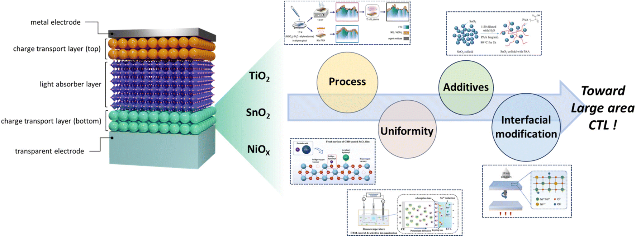 | ||
| Fig. 1 Schematic PSC structure and illustration of requirements toward large-area CTL. | ||
2. ![[thin space (1/6-em)]](https://www.rsc.org/images/entities/h3_char_2009.gif) Recent progress in deposition methods
Recent progress in deposition methods
2.1. Solution processed method
Solution processing offers a cost-effective, low-energy-consuming, and straightforward approach to deposit metal oxides for CTLs compared with other techniques such as sputtering,25–27 electron beam evaporation,28 atomic layer deposition (ALD),29,30 and pulsed laser deposition.31,32 Considering these advantages, numerous researchers have attempted to develop efficient solution-processed methods tailored for large-area CTL applications. Various solution-based deposition methods have been employed (Fig. 2), including spin coating, bar coating, spray coating, and chemical bath deposition (CBD). These solution processes can be broadly categorized into two approaches. The first involves coating a metal oxide thin film by spreading a solution containing either nanoparticles (NPs) or dissolved precursors, followed by drying and annealing. The second approach involves growing metal oxides in a chemical bath consisting of multiple reactants and precursors, requiring supplementary energy inputs, such as thermal or electrical energy. Among the methods, spin coating is the most frequently used for CTL fabrication due to its simplicity, especially for small-area cell production. However, its suitability for large-area CTL applications is often challenged, mainly due to the non-uniform film thickness resulting from centrifugal forces, potentially hindering optimal charge transport. Furthermore, spin coating approaches can lead to various morphological defects, including pinholes, partial voids, and inconsistent thickness.33 These defects can often be attributed to variations in the surface energy and the intrinsic roughness of TCOs, including fluorine-doped tin oxide (FTO) and indium tin oxide (ITO). Despite these limitations, spin-coated TiO2-based perovskite mini-modules (n–i–p devices) achieved a world-record certified PCE of 22.87% in 2022 using single crystalline TiO2 and remain in frequent use.34 In the following parts, we reviewed various solution process for up-scaling and strategies for large-area spin coating. In the sections that follow, we explore a range of solution processes geared towards up-scaling, along with strategies specifically designed for large-area spin coating.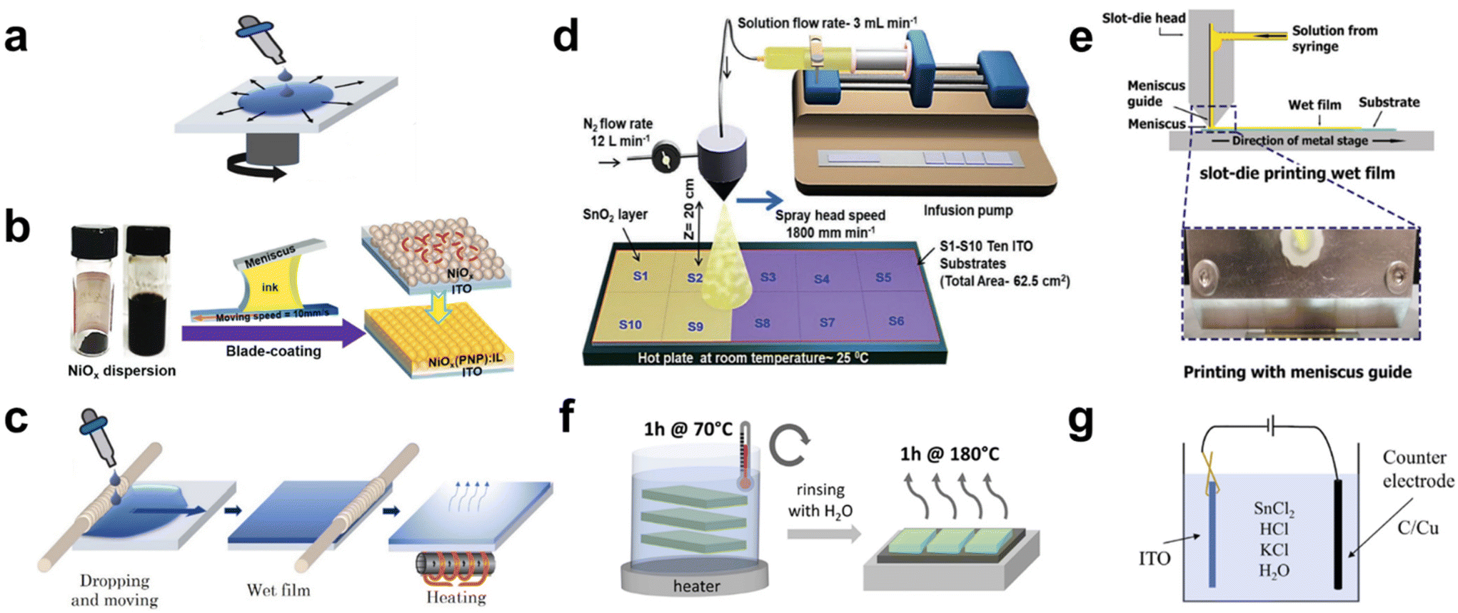 | ||
| Fig. 2 Illustrations of scalable solution process for metal oxide CTL. (a) Image for spin coating. Reproduced with permission.35 Copyright 2022, Elsevier. (b) Image for blade coating. Reproduced with permission.53 Copyright 2021, Wiley-VCH. (c) Image for bar coating. Reproduced with permission.35 Copyright 2022, Elsevier. (d) Image for spray coating. Reproduced with permission.37 Copyright 2022, Wiley-VCH. (e) Image for slot-die coating. Reproduced with permission.54 Copyright 2022, Wiley-VCH. (f) Image for chemical bath deposition (CBD). Reproduced with permission.44 Copyright 2022, American Chemical Society. (g) Image for electron chemical deposition (ECD). Reproduced with permission.46 Copyright 2023, Royal Society of Chemistry. | ||
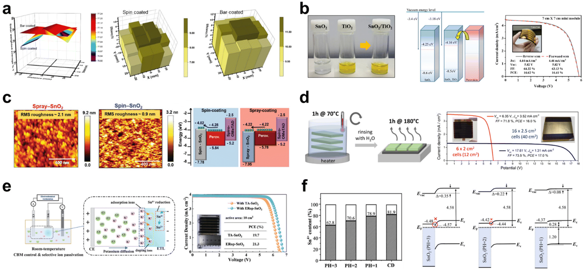 | ||
| Fig. 3 (a) 2D spatial mapping of solar weighted transmittance values (TSW) and PSC performance homogeneity of spin-coated and bar-coated mp-TiO2, respectively. Reproduced with permission.35 Copyright 2022, Elsevier. (b) Photograph of SnO2–TiO2 hybrid solution, schematic energy level diagram of ETLs, and J–V curve of flexible 7 × 7 cm2 mini-modules with its photograph. Reproduced with permission.36 Copyright 2022, American Chemistry Society. (c) Atomic force microscope (AFM) images and schematic energy level diagram of spin-coated and spray-coated SnO2, respectively. Reproduced with permission.37 Copyright 2021, Wiley-VCH. (d) Illustration of CBD deposition (left) and J–V curves of the optimized mini-modules (right). Reproduced with permission.44 Copyright 2022, American Chemistry Society. (e) Illustration of the electrochemical regulation method (left) and J–V curves of thermal annealed and electrochemical regulated SnO2-based mini-modules (right). Reproduced with permission.45 Copyright 2022, American Chemistry Society. (f) Schematic energy level and Sn4+ proportion of SnO2 ETLs prepared in different pH. (The Sn4+ proportion was calculated based on the XPS results.) Reproduced with permission.46 Copyright 2023, Royal Society of Chemistry. | ||
In a recent study on large-area ETLs implemented through spin coating, it was revealed that the SnO2–TiO2 hybrid ETL facilitates the development of efficient, flexible perovskite mini-modules using this coating technique.36 This hybrid ETL was synthesized by incorporating a TiO2 nanosol, which acts as an inorganic binder, into a SnO2 colloidal solution. Notably, the TiO2 nanosol comprises stably dispersed crystalline TiO2 NPs with dimensions smaller than 10 nm. An optimal balance was found when 5 wt% of TiO2 was added to a 3 wt% SnO2 colloidal solution, resulting in a peak efficiency of 21.88% in small cells. UPS findings indicated that an elevation in the energy level of the SnO2–TiO2 hybrid ETL led to an advantageous energy level alignment, thus driving a higher VOC value (Fig. 3b). Consequently, while the mini-module employing solely the SnO2 ETL displayed markedly low VOC and FF values, the mini-module based on the SnO2–TiO2 hybrid ETL achieved a PCE of 16.62% over an active area of 15 cm2. The pronounced efficiency variation across large areas between the SnO2 and SnO2–TiO2 ETLs indicates that the hybrid ETL offers a more consistent layer compared with the SnO2 ETL. This consistency is likely attributed to the effective role of the TiO2 nanosol as an inorganic binder. Additionally, in a bending resistance test with a bending radius of 5 mm, while SnO2-based f-PSCs showed ∼90% of the initial PCE after only 200 bending cycles, TiO2–SnO2-based f-PSCs maintained ∼90% of the initial PCE after 500 bending cycles.
Ding et al. reported a study on single-crystalline TiO2 (SC-TiO2) rhombus-like NPs with exposed (001) facets.34 These were synthesized through a one-step solvothermal method and employed as a large-area ETL. Impressively, the study reported a high certified efficiency of 22.72% over an active area of 24.63 cm2. The authors suggested that SC-TiO2 possesses superior conductivity and crystallinity, reduces interfacial charge recombination, and mitigates interfacial charge accumulation compared with commercial mp-TiO2. Furthermore, SC-TiO2 exhibited a decreased trap density and heightened electron mobility relative to mp-TiO2. Based on these advantages, devices utilizing SC-TiO2 achieved an enhanced fill factor exceeding 84%, ensuring efficient performance in both small-sized cells and mini-modules. Furthermore, they sustained roughly 90% of their initial efficiency over a span of 1400 hours. Consequently, TiO2 NPs with high crystallinity enable the fabrication of efficient and stable perovskite mini-modules, even when employing spin coating.
Spray coating offers another avenue for enhancing the scalability of CTL. Kumar et al. reported on the potential of room-temperature spray deposition for the fabrication of large-area SnO2 ETL-based PSCs.37 They successfully demonstrated that a SnO2 film measuring 62.5 cm2 could be deposited using a rapid, multi-pass spray deposition technique at room temperature. The morphological, surface analytical, electrical, and device properties of SnO2 were compared between the spin-coated and spray-coated methods, using commercial colloidal SnO2 dispersions. The spray-coated SnO2 exhibited a granular structure, indicative of a mesoporous morphology (Fig. 3c). This structure is advantageous for interfacial charge transfer, enhancing the contact area between the ETL and the perovskite.38 Notably, such a granular structure was absent in the spin-coated SnO2. From the XPS analysis, the spray-coated SnO2 film exhibited fewer oxygen defects, reduced C–C containing compounds, and a higher concentration of K ions compared with the spin-coated SnO2 film. The presence of K ions can reduce the defect density at the interface due to their passivation effect, promoting efficient interfacial charge transfer. To assess the performance of scaled-up SnO2 films in PSCs, substrates measuring 2.5 × 2.5 cm2 were sectioned into 10 pieces following the deposition of SnO2 on 62.5 cm2 ITO substrates. The highest efficiency for devices with spin-coated SnO2 was 16.01% over an active area of 1.0 cm2, whereas devices with spray-coated SnO2 achieved an efficiency of 18.90%. Furthermore, the spray-coated SnO2 devices across all 10 sections demonstrated remarkably consistent efficiencies, ranging narrowly between 19.11% and 20.08% in the active area of 0.096 cm2. This study indicates that the spray-coating method not only produces high-quality SnO2 with improved charge extraction and reduced recombination at the ETL/perovskite interface, yielding a lower trap density compared with spin-coated SnO2, but also offers advantages in scalability.
Taheri et al. reported the performance of SnO2-based perovskite solar modules, which were fabricated on flexible substrates utilizing the spray-coating method.39 Using water-based SnO2-NP dispersions in the spray coating method, they successfully deposited uniform and compact SnO2 films over a 120 cm2 area on flexible plastic substrates. These modules yielded power conversion efficiencies (PCE) of 12.0% and 11.7% for active areas of 16.8 cm2 and 21.8 cm2, respectively.
Zhang et al. explored the potential of a SnO2/SnOx bilayer ETL for large-area perovskite modules, employing ultrasonic spray coating at a low temperature (≤100 °C).40 For a well-defined large-area SnO2 layer using the spray coating method, they fine-tuned parameters such as substrate temperature, precursor flow rate, and co-solvent volume ratio. They further prepared a SnO2/SnOx bilayer by spraying a sol–gel of SnCl2 onto SnO2 to fill the voids and gaps in the SnO2 NP film. Notably, the residual chloride in the spray-coated sol–gel SnCl2 enhanced the Cl passivation effect, leading to improvements in both VOC and JSC. While this work did not specify the efficiency of the solar module, the high VOC of 6.1 V in modules with a 2.1 cm2 aperture area indicates that the SnO2/SnOx ETL exhibited good uniformity and homogeneity.
In the deposition methods employing colloidal solutions as described above, achieving a uniformly thick layer across large-area substrates is challenging due to the “coffee-ring effect”.41 This effect arises from varying solvent evaporation rates throughout the droplets,42 leading to capillary outflow. Optimizing coating conditions and refining solvent engineering to mitigate the unwanted coffee-ring effect requires significant effort. However, by directly growing a film on the substrate instead of using a colloidal solution, a more uniform film can be achieved, circumventing the challenges associated with the coffee-ring effect.
Recently, PSCs utilizing CBD SnO2 have achieved a remarkable certified power conversion efficiency of 25.2% in a small area, utilizing a straightforward method that incorporates urea, tin(II) chloride dihydrate, and acidic materials.43 Subsequently, the CBD method has emerged as a promising approach for depositing SnO2, not only for highly efficient PSCs but also for achieving uniform films over large areas.
Zimmermann et al. attempted the fabrication of perovskite mini-modules using CBD SnO2 as the ETL. CBD SnO2 samples were prepared with 1, 2, and 3 cycles for 1 hour at 70 °C.44 This was due to the finding that a single cycle of the CBD reaction did not reliably yield an efficient ETL, primarily due to incomplete coverage of the FTO surface. The optimal reaction was achieved in 2 cycles, resulting in an efficiency of 19.2% in small cells. For uniform mini-module fabrication, the perovskite and HTL layers were prepared using slot-die coating. The PCEs of the mini-modules reached 16.0% and 17.0% for aperture areas of 6.0 × 2.0 cm2 and 16.0 × 2.5 cm2, respectively (Fig. 3d).
Interestingly, Bai et al. developed an innovative and efficient annealing-free strategy for SnO2 through simple electrochemical regulation.45 This method achieved an impressive mini-module PCE of 21.3% over an active area of 10 cm2 (Fig. 3e). The as-deposited CBD SnO2 was subjected to both thermal annealing and electrochemical regulation, termed TA-SnO2 and ER-SnO2, respectively. For TA-SnO2, the PCE decreased above 200 °C even though the conductivity increased with rising temperatures. The conduction band minimum (ECBM) of TA-SnO2, which shifted from −4.23 to −4.69 eV, did not align well with that of the perovskite. This indicates that the conductivity enhancement from heat treatment could not compensate for the energy loss due to obstructed electron transport. In contrast, through electrochemical regulation at room temperature, the ECBM of the ER-SnO2 can be modulated, leading to an enhanced band alignment in PSCs and subsequently improved the carrier extraction. Moreover, ER-SnO2 exhibited a higher carrier concentration and increased conductivity, attributed to the K ion doping effect during electrochemical regulation. Time-resolved photoluminescence (TRPL) results revealed that electrochemical regulation facilitates electron extraction at the perovskite/ETL interface and reduces radiative recombination. Consequently, all photovoltaic parameters of the mini-module with ER-SnO2 surpassed those of TA-SnO2-based devices, suggesting that electrochemical regulation holds promise for efficient large-area PSCs.
Beyond the CBD method, Sun et al. were the first to report on the electrochemical deposition (ECD) of polycrystalline SnO2 at room temperature for large-area perovskite solar cells.46 By controlling the pH of the electrolyte, this method allowed for the modification of the SnO2 work function, facilitating a better energy alignment with the perovskite layer. At the optimal pH value of 1, the device surpassed the performance of those made with commercial colloidal dispersion SnO2, achieving a PCE of 19.21% in the active area of 0.99 cm2. Regulating the presence of oxygen vacancies in SnO2 is crucial as it influences the electron carrier concentration.47 The proportion of Sn4+ increased with decreasing pH, suggesting that the ECD method could fine-tune the ratio of oxygen vacancies on the SnO2 surface via electrolyte pH control (Fig. 3f). Lower pH values led to greater work function values due to the diminished oxygen vacancies, culminating in a superior energy level alignment. While ECD SnO2-based mini-modules were not produced, smaller devices, created from 1.5 × 1.5 cm2 sections cut from a 10 × 10 cm2 SnO2 substrate, demonstrated consistent PCEs.
Chou et al. investigated a spray-coating technique for the large-scale deposition of NiOx.52 They introduced a scalable ultrasonic spray-coating technique and examined the optical and chemical alterations in the spray-coated NiOx following various post-annealing durations. In general, after NiOx deposition, a post-annealing process at elevated temperatures (ranging from 300 to 600 °C) is employed to eliminate organic components and enhance NiOx crystallinity. In this perspective, they presented a method that facilitates rapid, low-temperature annealing, resulting in a transparent and compact crystalline NiOx layer. As a result, under optimal annealing conditions, the mini-modules achieved a PCE of 6.18% with an aperture area of 10.4 cm2.
Moreover, Zhang et al. attempted to use the polymer network micro-precipitation method to address the agglomeration phenomenon observed in NiOx NPs (Fig. 4a).53 Through this method, they achieved enhanced uniformity in NiOx films characterized by monodispersed and crystalline NPs, enabling the use of the blade-coating technique for scalable NiOx fabrication. The optimally dispersed NiOx precursor yields a deposition that is both flatter and smoother than that derived from a non-optimized NiOx colloidal solution. The polymer grid effectively limits the mobility and growth of NiOx NPs during preparation. Concurrently, the polymer network method enhances charge extraction capabilities owing to the encompassing polymer grid. Furthermore, an ionic liquid (IL), 1-ethyl-3-methylimidazole diethyl phosphate, is integrated into the resultant NiOx NPs as a surfactant. The surfactant reduces nanoparticle agglomeration and enhances its conductivity. Additionally, the functional group (–P![[double bond, length as m-dash]](https://www.rsc.org/images/entities/char_e001.gif) O) of the IL passivates the underlying perovskite film by coordinating with the divalent Pb2+, leading to a more crystalline perovskite layer. With this approach, PCEs of 20.91% (a control PCE of 18.05%) and 19.71% (a control PCE of 16.50%) were achieved in rigid and flexible large-area substrates with 1.01 cm2, respectively.
O) of the IL passivates the underlying perovskite film by coordinating with the divalent Pb2+, leading to a more crystalline perovskite layer. With this approach, PCEs of 20.91% (a control PCE of 18.05%) and 19.71% (a control PCE of 16.50%) were achieved in rigid and flexible large-area substrates with 1.01 cm2, respectively.
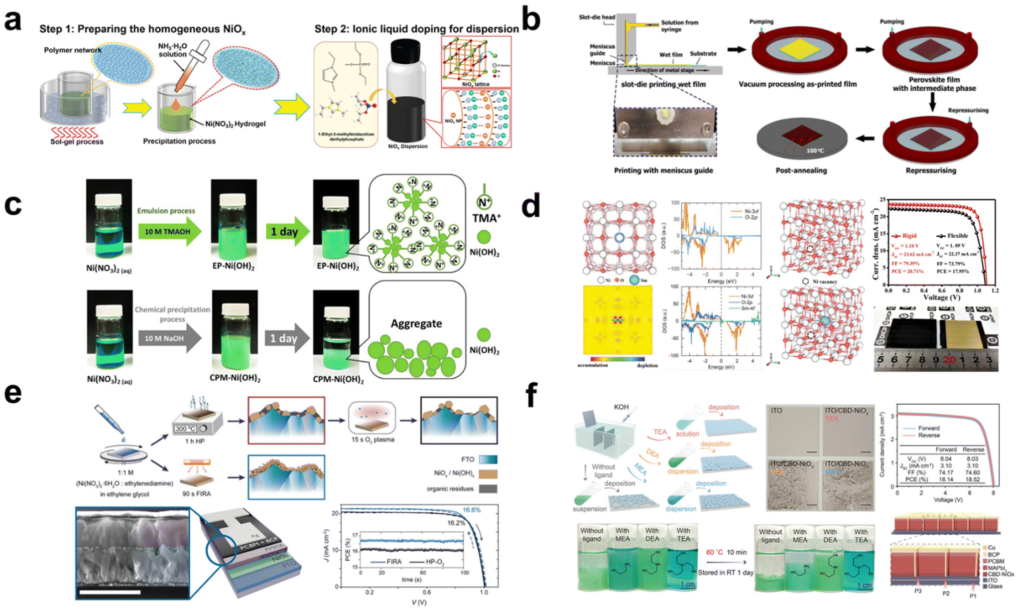 | ||
| Fig. 4 (a) Schematic figure of the polymer network micro-precipitation method and introduction of a surfactant IL. Reproduced with permission.53 Copyright 2021, Wiley-VCH. (b) Perovskite deposition method via slot-die coating with vacuum fast-assisted solution processing (VASP). Reproduced with permission.54 Copyright 2021, Wiley-VCH. (c) Schematic Illustration of well-dispersed Ni(OH)2 nanoparticles prepared by emulsion and chemical precipitation processes. Reproduced with permission.55 Copyright 2021, Elsevier. (d) Calculated crystal structure, charge density, partial density of states (DOS), and crystal structure including Ni vacancies. Typical J–V curves for the rigid and flexible devices with a large area. Reproduced with permission.56 Copyright 2021, Wiley-VCH. (e) Schematic illustration of the NiOx annealing process by a hot plate (HP) flash annealing (FIRA) process. Device structure, and J–V curve for FIRA and HP-O2. Reproduced with permission.58 Copyright 2023, Wiley-VCH. (f) Schematic figure of the NiOx formation process by different chemically structured amino alcohol ligands. J–V curves of PSM with the target CBD-NiOx. Device structure of PSM. Reproduced with permission.62 Copyright 2023 Wiley-VCH. | ||
The slot-die coating technique is also well-suited for the scalable fabrication of PSCs. PSCs fabricated entirely through slot-die coating have been demonstrated and executed under ambient conditions with a relative humidity (RH) of 20–40% and temperatures ranging from 15–20 °C (Fig. 4b).54 Critical to this process is a meticulous control over parameters such as the preheating temperature of the substrate and the film thickness, given the sensitive formation stages of NiOx. Furthermore, the addition of A-cation additives based on chlorides, specifically MACl and FACl, proves crucial during the slot-die coating of the perovskite film. This incorporation facilitates the achievement of an average grain size exceeding 400 nm, indicative of high crystallinity. Using the comprehensive slot-die process, champion PSCs measuring 1 cm2 and based on MAPbI3−xClx and CsFAPbI3−xClx achieved PCEs of 16.06% and 17.33%, respectively. Additionally, champion slot-die coated PSMs, having an active area of 2.1 cm2, registered PCEs of 11.7% for MAPbI3−xClx and 14.9% for CsFAPbI3−xClx.
In addition to the selection of a deposition method, a low-temperature process for NiOx is preferred for the fabrication of large-area devices. A recent study reports a low-temperature process (below 150 °C) for the synthesis of highly crystalline NiOx NPs.55 In this method, tetramethylammonium hydroxide (TMAOH) serves as a surfactant, facilitating the conversion of Ni(NO3)2 into Ni(OH)2 NPs (Fig. 4c). The resultant NiOx NPs, which exhibit outstanding dispersibility and stability, are synthesized through an emulsion process. The uniform NiOx films enhance the interfacial contact with the perovskite layer. As a result, impressive efficiencies of 18.85% and 13.93% were attained for devices with active areas of 0.09 cm2 and 1 cm2, respectively. This is in contrast to the control efficiencies of 16.68% and 10.06%. They also demonstrated a flexible PSC that achieved a PCE of 14.3%.
Recently, Wang et al. proposed a strategy to produce high-quality NiOx NPs using a low-temperature process.56 In the conventional low-temperature synthesis of NiOx NPs, the NO3− ion, which arises from the reaction between Ni(NO3)2 and NaOH, is identified as the predominant impurity in the NiOx film. This impurity cannot be completely removed at low temperatures. To address this issue, an ionic liquid-assisted synthesis approach (NiOx-IL) has been proposed. This method utilizes 1-butyl-3-methylimidazolium in place of the traditional Ni(NO3)2 precursor. This approach effectively facilitates the removal of impurity ions, such as NO3−, which tend to adsorb readily onto the surface of NiOx NPs, subsequently enhancing the conductivity of NiOx. The resultant NiOx layer also facilitates hole transfer, attributed to its improved extraction capability. The resulting device exhibits a PCE of 22.62%, a notable improvement compared with the control PCE of 19.80%. Remarkably, even the large-area device measuring 1 cm2 achieves a high PCE of 20.19%.
Beyond the typical monovalent and divalent ions, Bao et al. suggest that trivalent samarium-doped NiOx (Sm:NiOx) NPs, prepared using a chemical precipitation method, obviate the need for a post-annealing process.57 This study reveals that the Sm3+ dopant effectively reduces the formation energy of the Ni vacancy, implying its role in enhancing the p-type property of NiOx (Fig. 4d). As a result, the Fermi level is downshifted toward the valence band, enhancing electrical conductivity and facilitating carrier extraction at the perovskite/NiOx interface, which in turn minimizes the charge recombination loss. The chemical reaction of Sm:NiOx NP is illustrated using the following equations:
| Ni(NO3)2 + Sm(NO3)3 + NaOH → (NixSm1−x)(OH)2↓ | (1) |
| (NixSm1−x)(OH)2 → (NixSm1−x)Ox + H2O. | (2) |
Owing to the enhanced optoelectronic properties, devices structured as an ITO/Sm:NiOx/perovskite layer/PCBM/BCP/Ag achieve champion PCEs of 20.71% for an area of 0.09 cm2 and 18.51% for 1 cm2. Notably, since the deposition technique for Sm:NiOx obviates the need for a post-annealing process, a flexible plastic PSC has been introduced, achieving a PCE of 17.95%. Additionally, a large module has been developed using the blade-coating method to deposit the perovskite film. The PSM (40 × 40 mm2) yields a high PCE of 15.27% with the active area of 8.85 cm2 at the optimized Sm3+ concentration.
To ensure cost-effective mass production and expedited manufacturing, challenges related to the annealing temperature and the extended duration of the annealing process need to be addressed. Lian et al. reported a method for fabricating NiOx at temperatures below 82 °C using a UV irradiation strategy, which offers notable reductions in manufacturing costs.58 This UV irradiation effectively converts Ni2+ to Ni3+, modulating a deeper valence band that is advantageous for charge extraction from the perovskite film. The relevant chemical mechanism is proposed as a following reaction.
 | (3) |
A champion photovoltaic device fabricated using UV irradiation achieves a remarkable PCE of 22.45%, compared with a control PCE of 19.79%. Additionally, this approach has been applied to flexible PSCs, achieving a PCE of 19.7%.
Instead of the conventional annealing methods, such as those using a hot plate or furnace, an alternative approach is proposed. Ochoa-Martinez et al. introduce the flash infrared annealing (FIRA) process, which facilitates short annealing durations under ambient conditions (Fig. 4e).59 The FIRA method promotes the generation of excess oxygen in NiOx, leading to an elevated O/Ni ratio. This technique significantly enhances conductivity compared with the traditional hotplate annealing process. Consequently, impressive PCEs of 16.1% for a large area of 1 cm2 and 15.9% for a submodule area of 17 cm2 were recorded.
In regular structured PSCs that utilize SnO2 as the electron transport layer, the chemical bath deposition (CBD) method offers a significant enhancement in both performance and stability.20
However, when utilizing the CBD method for NiOx deposition, the efficiency in inverted PSCs was found to be suboptimal. The primary challenges with the CBD approach for NiOx include inconsistent grain sizes and low conductivity.60 To address these issues, it is imperative to fine-tune the grain size through controlled growth adjustments and enhance conductivity. Recently, a CBD method has been developed that allows for in situ growth tunability through different ligands.61,62 This method also enables a low-temperature process, contrasting with the traditionally required high annealing temperatures for NiOx deposition. Especially, it has been demonstrated that the controlled growth of NiOx can be adjusted by the ligand structure.63 The optimal ligand, tri-ethanolamine (T-EA), results in a uniform and compact deposition of NiOx (Fig. 4f). This method utilizes a brief exposure to a modest temperature of 270 °C, making it compatible with substrates like ITO that can be processed at low temperatures. They emphasize the benefits of this method, which facilitates both the mass production and scalable fabrication of solar modules. Consequently, impressive PCEs of 22.03% and 19.03% were achieved for devices with active areas of 0.1 cm2 and 18.10 cm2, respectively.
In addition to this, a copper (Cu) doped and seeding-induced crystallization approach (SCBD) is also introduced.60 By adopting the seed-assisted induction, a large grain size by controlled crystal growth is induced, resulting in a compact NiOx layer with lowered defect sites. In conjunction with the SCBD approach, a Cu-doping strategy is employed to promote the formation of shallow acceptor levels that function as defect states, enhancing both hole transport and conductivity. Utilizing an optimal Cu doping concentration, impressive PCEs of 22.51% and 19.29% were achieved for small (0.06 cm2) and large-area mini-modules (active area of 28 cm2), respectively.
2.2. Vacuum deposition
Considering the inherent limitations of general solution-processed deposition concerning surface morphology, uniformity, roughness, and coverage, the physical vapor deposition method offers a viable alternative. It ensures controllable thickness along with high conductivity. Furthermore, by adjusting doping concentration and modulating oxygen partial pressure, band structure tunability can be effectively facilitated, making it suitable for large-area manufacturing.64,65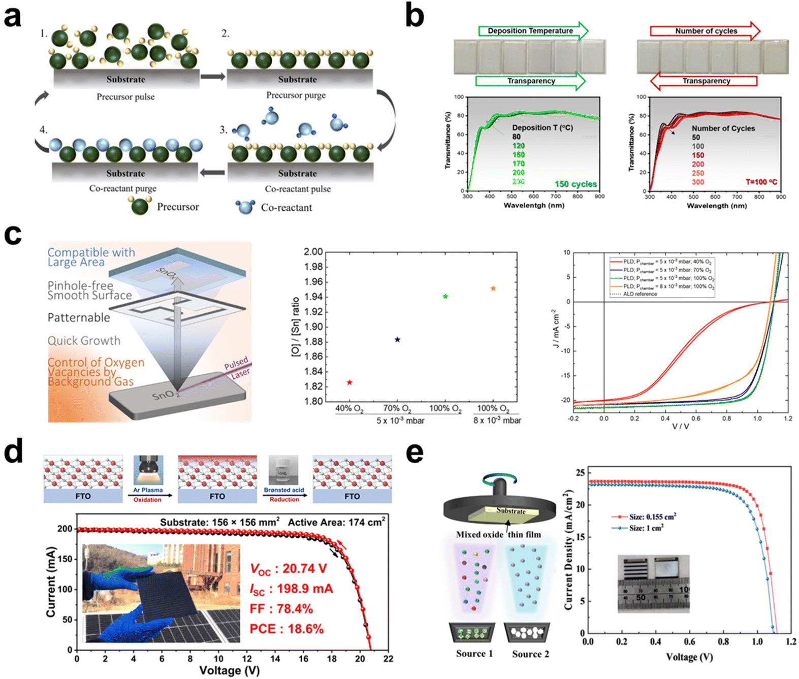 | ||
| Fig. 5 (a) Illustration of atomic layered deposition (ALD). Reproduced with permission.69 Copyright 2022, Wiley-VCH. (b) Transmittance of ALD SnO2 prepared with different temperatures and cycles. Reproduced with permission.30 Copyright 2021, Wiley-VCH. (c) Illustration of pulsed laser deposition (PLD) (left), O/Sn ratio (middle) and J–V curves (right) of SnOx (or devices) under different pressures and oxygen concentrations. Reproduced with permission.32 Copyright 2023, American Chemistry Society. (d) Schematic illustration of the process of surface redox engineering (SRE). The J–V curves for the PSM with an active area of 174 cm2. Reproduced with permission.66 Copyright 2022, Elsevier. (e) Schematic figure showing the dual-source electron beam co-evaporation process. The J–V curves for the PSCs with an active area of 0.155 and 1 cm2, respectively. Reproduced with permission.67 Copyright 2022, Wiley-VCH. | ||
Zanoni et al. utilized the pulsed laser deposition (PLD) technique for SnO2 fabrication.32 The PLD method is acknowledged for its scalability, pattern ability, and rapid processing capabilities. They optimized both the PLD chamber pressure and the concentration of oxygen in the background gas (Fig. 5c). A deposition pressure of 5 × 10⁻³ mbar was found ideal for producing a smooth, pinhole-free PLD SnO2 layer. Additionally, an atmosphere saturated with 100% O2 was identified as crucial to mitigate the formation of oxygen vacancies. As a result, PLD enabled consistent deposition across extensive areas, spanning over 615 cm2, with a mere 1.5% variation in thickness.
| NiO2 + HNO3 → Ni4+ + H2O + NO3− → Ni≤3+ + O2 + NO3− | (4) |
| NiO or Ni2O3 + HNO3 → Ni≤3+ + H2O + NO3− | (5) |
| Ni(OH)2 or NiOOH + HNO3 → Ni≤3+ + H2O + NO3− | (6) |
Besides the SRE method on NiOx films, it is also imperative to achieve high-crystalline perovskite films. The slot die coating method is applied for the deposition of the perovskite, in which due to the increase of the surface-free energy of the SRE-treated NiOx, the contact angle is significantly lowered to ∼7°. The improved wettability facilitates the full coverage of the perovskite solution, which satisfies the difficult requirement of the slot-die coating. In this progress, an excellent PCE of 23.4% attributed to by an improved VOC and FF is obtained. As a result, this yielded PCEs of 23.4% and 18.6% in small-area and mini-modules (156 × 156 cm2), respectively.
Jiang et al. have introduced a scalable electron-beam co-evaporation method applicable for all-inorganic charge transport layers, including NiO and niobium oxide (Nb2O5), serving as an HTL and ETL, respectively (Fig. 5e).67 They propose mechanisms for enhancing electrical conductivity through the use of dopants such as Cu and tungsten (W). Through optimal dopant incorporation, copper-doped NiOx (Cu-NiOx) and tungsten-doped Nb2O5 (W-Nb2O5) exhibit improved charge transport abilities and effectively prevent halide segregation. These factors contribute to achieving high PCEs of 21.31% and 19.01% for active areas of 0.155 cm2 and 1 cm2, respectively.
2.3. Bilayer
He et al. proposed that a ZnO–SnO2 cascaded ETL enables the efficient fabrication of large-area perovskite solar modules using a combination of spray-coated ZnO and blade-coated SnO2.69 The perovskite layer and HTL for the modules were also prepared through blade coating. The ZnO–SnO2 ETL configuration effectively prevented the protonation of ZnO and established a well-matched conduction band level between the ETL and the perovskite layer, resulting in an improvement in the VOC. The use of a spray pyrolysis-coated ZnO underlayer prevented unfavorable physical defects (such as pinholes and partial coverage shortages) that can arise due to the toughness of FTO, in comparison with the blade-coated SnO2. The champion modules achieved efficiencies of 17.82% and 16.60% for active areas of 18.0 cm2 and 47.0 cm2, respectively.
Kim et al. reported a study on the utilization of polyacrylic acid (paa)-stabilized QD-SnO2 deposited on a c-TiO2 blocking layer to achieve a highly efficient ETL.70 This was accomplished through spin coating for paa-QD-SnO2 and spray pyrolysis for c-TiO2. The QD-SnO2 exhibited varying thicknesses, ranging from ∼30 nm to ∼70 nm, on the c-TiO2 layer, while the paa-QD-SnO2 demonstrated a uniform and conformal thickness of approximately ∼30 nm. This suggests that the paa played an important role in ensuring uniformity in the paa-QD-SnO2 ETL. The paa effectively interacted and bonded with the QD-SnO2, contributing to the formation of a conformal ETL (Fig. 6a).
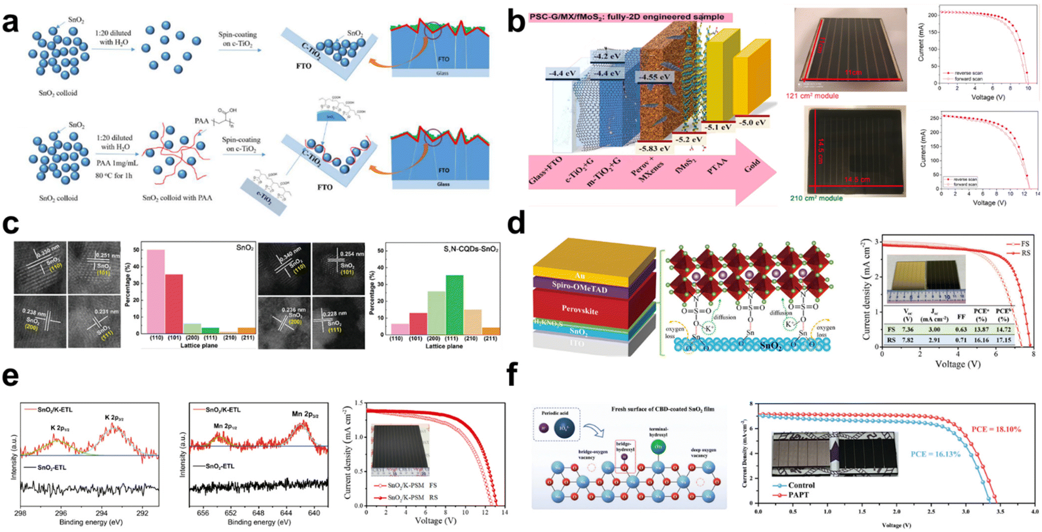 | ||
| Fig. 6 (a) Schematic diagram of the formation of QD-SnO2 and paa-QD-SnO2. Reproduced with permission.70 Copyright 2022, American Association for the Advancement of Science. (b) Structure of energy band diagrams (left), photographs and J–V curves of the champion mini-modules with different areas. Reproduced with permission.71 Copyright 2022, Elsevier. (c) HAADF-STEM images and the corresponding proportion of each exposed crystal plane of SnO2 and S,N-CQD-SnO2, respectively. Reproduced with permission.72 Copyright 2023, Wiley-VCH. (d) Illustration of ETL/PVSK interface passivation with H2KNO3S in the perovskite solar cells and J–V curves of the 5 × 5 cm2 champion mini-modules. Reproduced with permission.76 Copyright 2023, Wiley-VCH. (e) XPS spectra of SnO2 and SnO2/K (left) and J–V curves of SnO2/K-based mini-modules. Reproduced with permission.78 Copyright 2021, Springer Nature. (f) Schematic images of the periodic acid post-treatment on the SnO2 surface (left) and the J–V curves of the 3 × 3 cm2 control and target mini-modules, respectively (right). Reproduced with permission.80 Copyright 2023, Wiley-VCH. | ||
The best PCEs for mini-modules with active areas of 20 cm2 and 64 cm2 were found to be 21.7% and 20.6%, respectively. Moreover, an extended shelf-life test over 1000 h was conducted under ambient conditions with a relative humidity of 25% and a temperature of 25 °C. During this test, the paa-QD SnO2@c-TiO2-based perovskite solar cells retained approximately 80% of the initial PCE of 25.7%. The researchers not only addressed the limitations associated with spin coating through additive engineering for the SnO2@TiO2 bilayer fabrication but also achieved remarkably high efficiency for large-area mini-modules.
2.4. Interfacial modification
Pescetelli et al. employed 2D materials to modify interfaces within perovskite modules.72 Specifically, they utilized graphene ink for c-TiO2 and mp-TiO2 layers, MXenes for the perovskite layer, and fMoS2 for the perovskite/PTAA interlayer (Fig. 6b). The inclusion of graphene in the ETL notably improved the electron mobility and electron injection at the mp-TiO2/perovskite interface, and simultaneously reduced the charge trap sites within the mp-TiO2. This led to an enhanced FF and an increased open-circuit voltage VOC. Based on these improvements, they highlighted the potential of 2D materials in countering the inefficiencies typically introduced during scaling-up. In their optimized perovskite solar modules featuring 2D materials, the champion device achieved a 17.2% and 14.7% PCE for 121 cm2 (the active area of 82.62 cm2) and 210 cm2 (the active area of 137.2 cm2) modules, respectively (Fig. 6b). Moreover, the 121 cm2 modules, encapsulated via a glass sealing technique, maintained 80% of their initial PMAX values after approximately 530 h at 85 °C. Regarding the improved stability, they proposed that (1) the stable perovskite crystal structure within the mp-TiO2 + graphene matrix contributed to the temperature stabilization of the charge carriers, and (2) the transformation of perovskite into PbIx and PbOx species might be slowed down by the presence of graphene within the mp-TiO2.
To further develop the CBD TiO2, Guo et al. reported poly-L-lysine with modified sulfonic acid groups (PLLS) for the TiO2/perovskite interface.73 Not only did the sulfonic acid groups reduce the oxygen vacancies of the TiO2 surface, leading to an increase in conductivity, but also the amine groups passivated deep-level defects of perovskite, resulting in a reduction of non-radiative recombination. Thus, a high PCE of 20.07% with a notable FF of 76.75% was obtained in the active area of 33 cm2. Importantly, no voltage loss was observed during the scaling-up process. In terms of stability, the PLLS-modified mini-modules retained 80% of their initial PCE for 30 days under ambient conditions at room temperature and an RH of 5–10%. In contrast, the control mini-modules only managed to retain 60% of their initial PCE for a mere 6 days.
Among efforts to further improve spin-coated SnO2, Yang et al. reported how altering the SnO2 crystal facet with a novel carbon quantum dot (CQD) doping technique could yield highly efficient PSCs.74 The CQD-doped SnO2 predominantly featured the (200) and (111) facets, in contrast to the pristine SnO2, which was characterized by the (110) and (101) facets (Fig. 6c). Considering that the adsorption energy of Pb2+ is higher on the more active (200) and (111) crystal planes, perovskite crystal nucleation is enhanced on the CQD-SnO2 surface. Besides, the buried perovskite/CQD-SnO2 interface was observed with better crystallinity than that of pristine SnO2. Flexible mini-modules based on CQD-SnO2 attained a PCE of 17.79% over an aperture area of 24 cm2. These modules also demonstrated superior stability, preserving approximately 95% of the initial PCE for 1200 h at 25 °C and an RH of around 40% under 1-sunlight exposure, and retained >90% of the initial PCE after bending cycles with a bending radius of 6 mm.
In a separate study, Hu et al. modified the SnO2/perovskite interface with diphenyl phosphine oxide (DPO), a phosphorus-containing Lewis acid.75 This resulted in an impressive PCE peak of 15.69% for mini-modules covering an aperture area of 22.56 cm2. They reported that the Lewis acid sites of the DPO engaged with the SnO2 surface, neutralizing OH– groups. This interaction considerably enhanced electron transfer and diminished the energy barrier between the perovskite and SnO2 layers.
Tong et al. introduced potassium sulfamate (H2KNO3S) as a modification to the SnO2/perovskite interface (Fig. 6d).76 Their aim was to mitigate the oxygen loss from SnO2 encountered during the hybrid chemical vapor deposition (HCVD) process, a method intended for scalable perovskite fabrication. While the HCVD technique holds promise for large-scale perovskite deposition, they identified an issue: SnO2 experienced oxygen loss during this deposition process, leading to interfacial defects and enhanced carrier recombination. By introducing H2KNO3S, they established a chemical bridge between the SnO2 and perovskite layers. This not only compensated for the oxygen loss but also passivated the uncoordinated Pb2+ within the perovskite. The result was more than just a surface modification of SnO2; it effectively addressed challenges inherent in large-area perovskite deposition. As a result, PCEs of 16.16% and 12.12% were achieved for active areas of 22.4 cm2 and 91.8 cm2, respectively.
While the CBD method is a promising method for SnO2 deposition, challenges remain, such as the need to reduce the inherent defect density, eliminate interfacial defects, and ensure uniform coverage for scalable SnO2 ETL. Addressing these, several strategies have been developed to introduce additives into the chemical bath solutions. For instance, Dong et al. incorporated potassium citrate into the CBD solution to optimize SnO2 coverage.77 Through this additive engineering, they successfully achieved a PCE of 24.84%, in small cells.
Tong et al. incorporated KMnO4 into the chemical bath solution to enhance the quality of SnO2.78 This addition also facilitated the doping effects of K and Mn ions as they diffused into the upper perovskite grain boundaries. KMnO4 reduced the trap densities and enhanced carrier mobilities of SnO2 by promoting the oxidation of Sn2+ → Sn4+. Furthermore, they proposed that the formations of KCl and MnCl2 on the SnO2 surface served as effective passivators. Consequently, the K ions enabled the growth of larger perovskite grains, while the Mn ions enhanced perovskite crystallinity and phase stability due to their doping contributions. The resulting mini-modules, with active areas of 22.4 and 91.8 cm2, achieved PCEs of 17.26% and 13.72%, respectively (Fig. 6e).
Besides additive engineering, interfacial engineering presents another way for enhancement. Lv et al. employed hypervalent potassium xanthate (KiPX) to modify SnO2, aiming to minimize the interfacial defects and improve charge extraction in perovskite solar modules.79 The Lewis acid sites of the KiPX established robust interactions with both Pb2+ from the perovskite and Sn4+ from the SnO2. Furthermore, the release and diffusion of K ions from the KiPX into the perovskite grain boundaries served to passivate defect sites. As a result, the KiPX-modified mini-modules exhibited a stabilized efficiency of 18.8% over a 48.0 cm2 active area and retained 90% of their PCE after 600 h under ambient conditions.
Wu et al. demonstrated that periodic acid could interact with the hydroxyl groups present on the SnO2 surface (Fig. 6f).80 This interaction results in a more favorable energy level alignment between SnO2 and perovskite, leading to decreased interfacial non-radiative recombination and improved charge transport. A strong oxidation state of IO6− enabled the oxidation of Sn2+ → Sn4+ of SnO2, which led to reduced trap states and a higher VOC. As a result, the resultant mini-modules with the aperture area of 2.29 cm2 exhibited a high PCE of 18.10% (Fig. 6f). In a 3000 h shelf life test, the unencapsulated mini-modules retained 93.32% of their initial PCE under ambient conditions at 20 °C and a relative humidity of 20–25%. In contrast, the control mini-modules preserved only 29.79%.
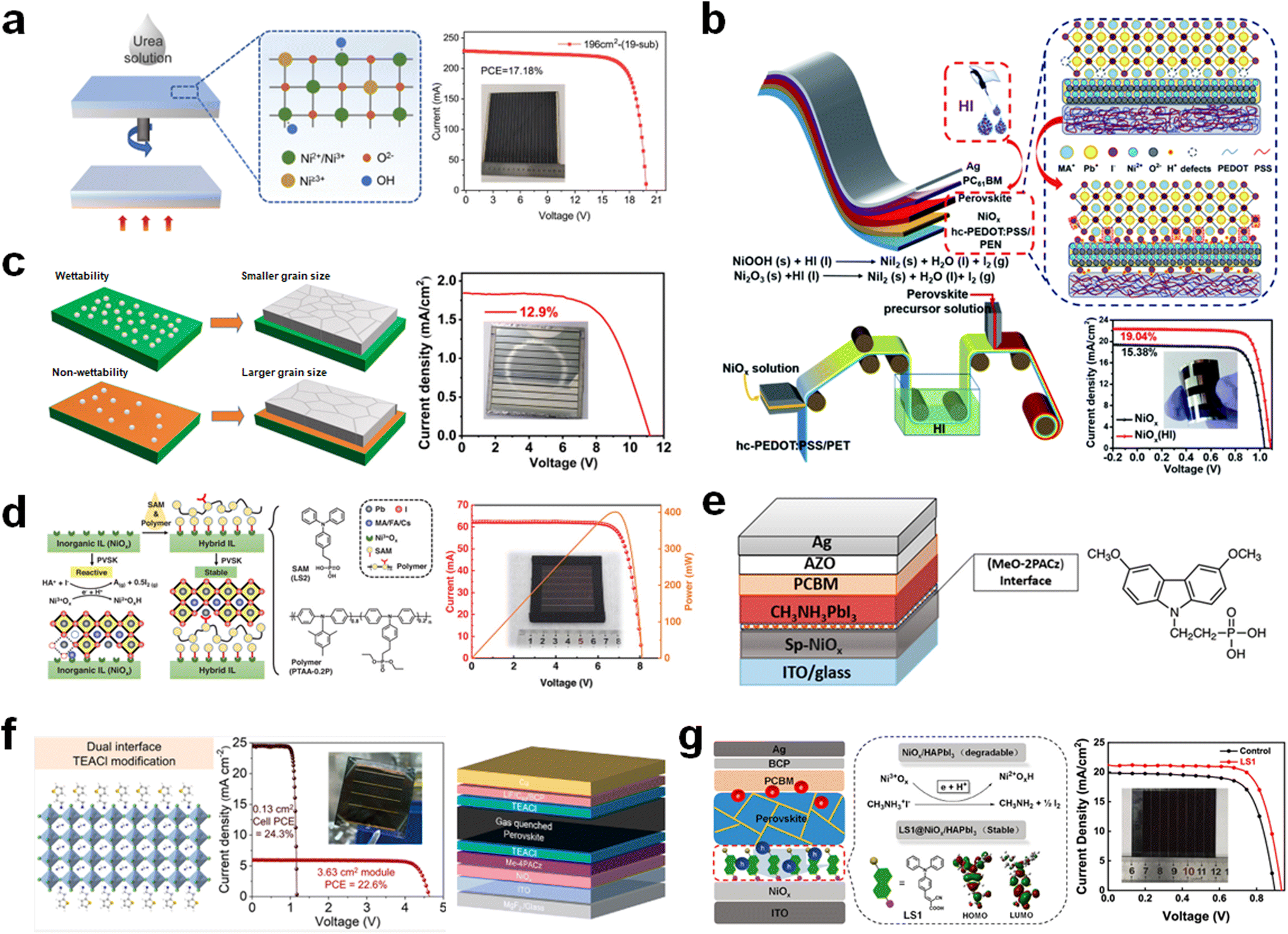 | ||
| Fig. 7 (a) Schematic illustration of the post treatment of urea. J–V curves for the PSM (area of 196 cm2). Reproduced with permission.81 Copyright 2023, Wiley-VCH. (b) Fabrication of the PSCs by an R2R process. J–V curves for the HI-treated and control devices. Reproduced with permission.82 Copyright 2021, The Royal Society of Chemistry. (c) Perovskite crystallization with a large grain size by TeDA-treated NiOx. J–V curves for the PSM (area of 53.64 cm2). Reproduced with permission.83 Copyright 2022, Wiley-VCH. (d) Hybrid interfacial strategy optimized by bilateral surfaces of CTL and a perovskite. A P–J–V curve of PSM on a hybrid IL (aperture area of 19.4 cm2). Reproduced with permission.84 Copyright 2023, Wiley-VCH. (e) Schematic illustration of the introduced MeO-2PACz as an interface in the device architecture. MeO-2PACz molecule structure. Reproduced with permission.89 Copyright 2022, American Chemical Society. (f) Schematic figure of the TEACl modification. Device architecture. Reproduced with permission.91 Copyright 2023, American Chemical Society. (g) Schematic illustration of suppressing perovskite decomposition by LS1. J–V curves for the LS1-treated and control perovskite solar modules (aperture area of 19.16 cm2). Reproduced with permission.96 Copyright 2022, American Chemical Society. | ||
Meanwhile, Wang et al. demonstrate the interface passivation strategy via HI soaking on NiOx in process of the roll-to-roll (R2R) technology (Fig. 7b).82 After treatment with HI, Ni3+ is reduced to NiI2 product by the following redox reactions.
| Ni(OH)2(s) + HI(l) → NiI2(l) + H2O | (7) |
| Ni2O3(s) + HI(l) → NiI2(l) + H2O(l) + I2(g) | (8) |
The reduced Ni3+ forms a favorable band alignment with better charge transport ability. Simultaneously, the resultant NiI2 product contributes to coordinating with Pb2+ in the perovskite film, which improves the perovskite quality and impedes the degradation reaction. Furthermore, it is found that the HI treatment is conducive for the adopted printing method due to the smoothened surface of the NiOx film. Eventually, the PCEs of the flexible PSCs show 19.04% (1 cm2) and 16.15% (15 cm2), respectively, which retain their initial PCE of 80% with a bending radius of 3 mm after 500 bending cycles.
Liu et al. discovered that TeDA modulates the wettability of the NiOx surface, impeding the crystallization process of the perovskite film (Fig. 7c).83 This leads to the deposition of a film characterized by larger grains and fewer defect sites. The TeDA treatment increases the contact angle to 87.1°, which manipulates the surface energy, resulting in the non-wetting surface leading to slow crystallization. As a result, a PCE of 12.9% is achieved for the module with an aperture area of 53.64 cm2 on spray-coated NiOx by surface engineering with the organic amine of TeDA.
Recently, a synergistic strategy has been introduced that both enhances the interfacial charge transport ability and improves the chemical stability.84 This approach involves a multifunctional thin layer that incorporates LS2 and PTAA-0.2P. This layer passivates NiOx by interacting with the dangling bonds on the metal oxide and coordinates with Pb2+ in the perovskite film (Fig. 7d). This hybrid interfacial strategy refines the chemical composition, boosts the carrier extraction ability, and results in optimal energy band alignment. Consequently, a solar module with an aperture area of 19.4 cm2 achieved a PCE of 20.7%.
For inverted flexible PSCs, low-temperature processed NiO is commonly utilized due to the robust chemical stability, high transmittance, and low manufactural cost. However, the processed NiO intrinsically possesses high defect sites and energy band mismatch with the perovskite film, thereby hindering the efficiency of the flexible PSCs. Beyond the intrinsic limit of single-junction PSCs, a tandem PSC with mitigated major interfacial problems such as non-radiative recombination and energy level mismatch is reported.85 The mixed molecules for bridging with 2PACz and MeO-2PACz tune the energy-level alignment between the NiOx and the perovskite and improve the charge extraction with mitigated interfacial recombination. Consequently, a large flexible device with an aperture area of 1.05 cm2 shows a high PCE of 23.5%, which retains the initial PCE after 10![[thin space (1/6-em)]](https://www.rsc.org/images/entities/char_2009.gif) 000 bending cycles with a maximum bending radius of 15 mm.
000 bending cycles with a maximum bending radius of 15 mm.
Recently, efforts to surpass the Shockley–Queisser limit for single-junction solar cells have intensified, with perovskite-silicon tandem solar cells emerging as a focal point of research. The CTLs and their associated interfacial layers are pivotal for tandem device operation, particularly in terms of charge transport and transmittance.86 In the context of CTL and TCO selection, SAMs have been introduced to minimize the Voc deficit and ensure optimal charge transfer.87 In recent advancements, IZO has been adopted as a TCO and 2PACz as an HTL. It has been demonstrated that a homogeneously anchored SAM on TCO achieves compact coverage, subsequently boosting the Voc and FF. Additionally, PTAA has been chosen to regulate the charge extraction of NiOx through π–π stacking.88
The MeO-2PACz interlayer is also utilized solely for the surface modification of NiOx.89 The modified interface enhances the quality of the perovskite film, with its well-structured band facilitating efficient charge transfer (Fig. 7e). This reduces the charge recombination due to the interfacial passivation effect on the NiOx. Consequently, a PCE of 16.25% is achieved over an active area of 1 cm2.
Ammonium salts which generally form 2D perovskite materials have been used for passivation within buried perovskite and NiOx.90 2-Thiolpheneethylammonium chloride (TEACl) is incorporated in both sides of the perovskite layer (i.e., buried, and top interfaces) (Fig. 7f).91 The TEACl-based dual interfaces contribute to the optimal band alignment and reduced defect sites, and improve interfacial contact, resulting in a high photovoltaic performance. The TEACl dual-treated PSC exhibits a PCE of 22.6% for the large submodule with an active area of 3.63 cm2.
It is crucial to mitigate the adverse interfacial reactions between NiOx and the perovskite film to prevent detrimental changes.92,93 Redox reactions, which lead to perovskite decomposition, and UV-induced degradation are both strongly associated with the degradation of the NiOx–perovskite interface.94 Interfacial treatment using SAM molecules is also an effective strategy.95 Liu et al. utilizes a self-assembled dyad molecule to reduce the redox reaction between Ni3+ and ammonium iodide composited in a perovskite film (Fig. 7g).96 A new self-assembled dyad molecule effectively suppresses the interfacial degradation and assists in modulation of the perovskite growth and charge extraction. Consequently, a PCE of 14.90% is obtained for the large module with an aperture area of 19.16%. Furthermore, as an integrated system to improve interfacial properties such as contact problems and carrier extraction, A-site cation-size mismatch and interface stabilization (CM-IS) strategies are introduced to achieve highly effective and stable PSCs.97 The integrated strategy facilitates the charge transport and improves interface contact in inverted PSCs. The surface modification of PTAA onto NiOx enhances the hole transport and suppresses the trap states of the NiOx. The further modification of mesoporous alumina (mp-Al2O3) on PTAA not only facilitates effective interfacial contact but also enhances charge extraction. As a result, in large area PSM (11.2 cm2), a PCE of 16.9% is achieved.
3. Conclusions
This review provides a comprehensive overview of metal oxide CTLs tailored for large-area PSMs in recent years. With impressive progress in PCE for both regular and inverted structured PSCs, the urgency for commercialization to support mass and large-scale production has grown. Considering this trend, there is a pressing need to focus on metal oxide CTLs for the development of large-area PSCs as shown in Table 1 and Fig. 8.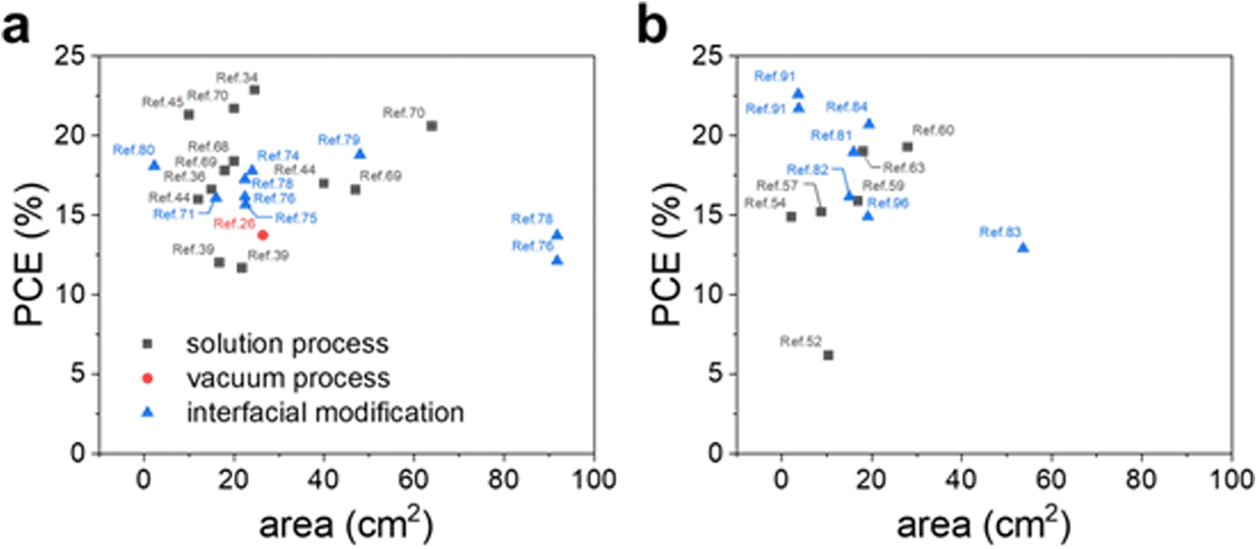 | ||
| Fig. 8 The efficiency of (a) n–i–p and (b) p–i–n structured metal oxide-based PSMs over 1 cm2 of the active or aperture area reported recently. | ||
| Device type | Metal oxide CTLs | Deposition method | PCE (%) | Area (cm2) | Reported kinds of area | Ref. |
|---|---|---|---|---|---|---|
| n–i–p | SnO2–TiO2 | Spin coating | 16.62 | 15 | Active | 36 |
| n–i–p | c-TiO2/SC-TiO2 | Spin coating | 22.87 | 24.63 | Active | 34 |
| n–i–p | SnO2 | Spray coating | 12.0/11.7 | 16.8/21.8 | Active | 39 |
| n–i–p | SnO2 | Chemical bath deposition | 16.0/17.0 | 6.0 × 2.0/16.0 × 2.5 | Aperture | 44 |
| n–i–p | SnO2 | Chemical bath deposition | 21.3 | 10 | Active | 45 |
| n–i–p | SnO2 | Atomic layer deposition | 13.74 | 26.4 | Active | 30 |
| n–i–p | SnO2/Acac-TiO2 | Spin coating | 18.39 | 20 | Aperture | 68 |
| n–i–p | ZnO2/SnO2 | Spray/blade coating | 17.8/16.6 | 18/47 | Active | 69 |
| n–i–p | c-TiO2/SnO2 | Spray/spin coating | 21.7/20.6 | 20/64 | Active | 70 |
| n–i–p | c-TiO2/mp-TiO2 | Spray/spin coating | 16.1 | 16 | Active | 71 |
| n–i–p | SnO2 | Spin coating | 17.79 | 24 | Aperture | 74 |
| n–i–p | SnO2 | Chemical bath deposition | 15.69 | 22.56 | Aperture | 75 |
| n–i–p | SnO2 | Spin coating | 16.16/12.12 | 22.4/91.8 | Active | 76 |
| n–i–p | SnO2 | Chemical bath deposition | 17.26/13.72 | 22.4/91.8 | Active | 78 |
| n–i–p | SnO2 | Chemical bath deposition | 18.8 | 48 | Active | 79 |
| n–i–p | SnO2 | Chemical bath deposition | 18.1 | 2.29 | Aperture | 80 |
| p–i–n | NiOx | Spray coating | 6.18 | 10.4 | Aperture | 52 |
| p–i–n | NiOx | Blade coating | 20.19/19/7 | 1.01 (rigid/flexible) | — | 53 |
| p–i–n | NiOx | Slot die coating | 14.9 | 2.1 | Active | 54 |
| p–i–n | NiOx NPs | Spin coating | 13.93 | 1 | Active | 55 |
| p–i–n | NiOx NPs | Spin coating | 20.19 | 1 | — | 56 |
| p–i–n | Sm:NiOx NPs | Spin coating | 18.51/15.2 | 1/8.85 | Active | 57 |
| p–i–n | NiOx | Spin coating | 16.1/15.9 | 1/17 | — | 59 |
| p–i–n | NiOx | Chemical bath deposition | 19.03 | 18.1 | Active | 63 |
| p–i–n | Cu:NiOx | Chemical bath deposition | 19.29 | 28 | Active | 60 |
| p–i–n | NiOx | Electron beam evaporation | 18.6 | 156 × 156 | Substrate | 66 |
| p–i–n | Cu:NiOx | Electron beam co-evaporation | 19.01 | 1 | Active | 67 |
| p–i–n | NiOx | Spray pyrolysis | 18.97/17.18 | 16/196 | Active | 81 |
| p–i–n | NIOx | Roll-to-roll fabrication | 19.04/16.15 | 1/15 | Active | 82 |
| p–i–n | NiOx | Spray coating | 12.9 | 53.64 | Aperture | 83 |
| p–i–n | NiOx | Spin coating | 20.7 | 19.4 | Aperture | 84 |
| p–i–n | NiOx | Spin coating | 23.5 | 1.05 | Aperture | 85 |
| p–i–n | NiOx | Sputtering | 16.25 | 1 | Active | 89 |
| p–i–n | NiOx | Spin coating/sputtering | 22.6/21.7 | 3.63/3.78 | Active | 91 |
| p–i–n | NiOx | Spin coating | 14.90 | 19.16 | Aperture | 96 |
| Device type | Organic CTLs | Deposition method | PCE (%) | Area (cm2) | Reported kinds of area | Ref. |
|---|---|---|---|---|---|---|
| n–i–p | Spiro-Naph | Spin coating | 21.83 | 25 | Aperture | 98 |
| n–i–p | Spiro-OMeTAD | Spin coating | 19.16 | 16.38 | Active | 99 |
| n–i–p | Spiro-OMeTAD (PPO-TEMPO) | Spin coating | 21.4 | 17.1 | Aperture | 100 |
| n–i–p | PTAA (OATFSI) | Spin coating | 19.91 | 209.39 | Active | 101 |
| p–i–n | MPA-CPA | Spin coating | 22.0 | 9.66 | Active | 102 |
| p–i–n | TPT-P6 | Spin coating | 20.09 | 1 | Active | 103 |
| p–i–n | Enantiomer-pure | Spin coating | 20.1 | 36.4 | Active | 104 |
This review highlights several critical aspects that must be addressed to enhance the efficiency, stability, and scalability of PSCs. Foremost among these is the need for spatial uniformity and reproducibility to ensure scalability. Moving beyond spin-coating, techniques such as bar, spray, blade, and slot die-coating emerge as potential solutions to issues of non-uniformity. However, the current volume of research on this topic is limited, and significant challenges persist, particularly when scaling up to larger module areas. Vacuum-based deposition entails higher costs and demands specialized facilities, but it remains a viable option for large-scale CTL fabrication due to its consistent uniformity and reproducibility. However, to date, only a limited number of studies have explored modifications to this deposition technique.
Strategies to regularly arrange metal oxide NPs can be beneficial for the up-scaling process. Introducing molecules acting as binders can promote the formation of a well-defined CTL with consistent thickness and fewer defects. Single crystalline or facet-controlled metal oxides also provide significant effects on large-area PSMs. The single crystalline NPs possess high conductivity as well as effectively suppress interfacial charge recombination and accumulation, leading to the narrow gap between the efficiencies of PSMs and small cells. Certain facet-controlled metal oxides tailor the activity of the metal oxide surface, which modulates the perovskite nucleation.
CBD is gaining prominence as a method for the large-scale production of SnO2 ETL. Through this approach, a uniform and homogeneous ETL is directly formed on the substrates within the chemical bath. The development of CBD can be readily tailored through adjustments in pH, the addition of chemicals, and other treatments such as thermal annealing. These manipulations offer potential for further refining of the morphological, optical, physical, and chemical properties of SnO2.
Considering that flexible polymer substrates necessitate low-temperature processes, there is a compelling need for research and development focused on low-temperature methodologies and associated materials to harness the full potential of PSMs. Unlike the high-temperature calcination required for TiO2, SnO2 and NiOx have recently emerged as promising CTL alternatives for large-area flexible PSMs due to their low-temperature processing capabilities. Additionally, while hybrid ETLs enable low-temperature annealing below 150 °C, methods employing electrochemical treatments also present the advantage of bypassing thermal annealing altogether.
The modulation of various properties through the use of additives and interfacial engineering is crucial for crafting CTLs suitable for scalable devices. These modifications play a pivotal role in influencing the optoelectrical, optical, and morphological attributes of the CTLs. In tandem with the passivation effects, the optimized energy band alignment significantly enhances carrier extraction, leading to reproducible device performance and enhanced stability. The enhanced electrical conductivity, stemming from an increased carrier concentration and mobility, is predominantly fine-tuned through this engineering approach, with a particular emphasis on NiOx refinement. Additionally, well-modified CTLs influence the perovskite grain growth rate and nucleation dynamics based on factors such as wettability and surface roughness, which, in turn, favor the formation of larger perovskite grains. A highly crystalline active layer significantly contributes to enhanced performance and stability, importantly influencing the scalability of PSMs. Introducing alkaline, transition, and halogen ions within CTL offers various benefits. These additives not only infiltrate the bulk perovskite layer, facilitating grain boundary passivation and modulating crystal growth, but they also chemically interact with interfacial defect sites, thereby diminishing trap densities.
The robust stability, which ensures reproducibility, is also important for solar modules exposed to external conditions, including thermal, humid, and light-illuminated environments. Approaches to inhibit the detrimental reactions at the perovskite/CTL interface through interfacial modifications are highly desired.
In summary, for the realization of mass-produced, large-area PSMs, continuous research and development efforts are essential to develop metal oxides that are both scalable and capable of achieving high performance. In this perspective, the target technology of metal oxides optimal for the scalable device is to secure low-temperature processes and low-cost facilities, which are necessary to achieve mass production. Even capabilities to ensure uniformity and reproductivity by connecting NPs with binders are expected to narrow the gap between large- and small-scale devices. To achieve this, there is still an urgent need to use various modification integrating additive, interfacial engineering, and deposition methods.
Conflicts of interest
There are no conflicts to declare.Acknowledgements
This work was supported by the DGIST R&D Program of the Ministry of Science and ICT (21-CoE-ET-01). This research was also supported by the National Research Council of Science & Technology (NST) grant by the Korea government (MSIT) (No. CAP 23070-017).References
- J. Park, J. Kim, H.-S. Yun, M. J. Paik, E. Noh, H. J. Mun, M. G. Kim, T. J. Shin and S. I. Seok, Controlled growth of perovskite layers with volatile alkylammonium chlorides, Nature, 2023, 616, 724–730 CrossRef CAS PubMed.
- Y. Zhao, F. Ma, Z. Qu, S. Yu, T. Shen, H.-X. Deng, X. Chu, X. Peng, Y. Yuan, X. Zhang and J. You, Inactive (PbI2)2RbCl stabilizes perovskite films for efficient solar cells, Science, 2022, 377, 531–534 CrossRef CAS PubMed.
- X. Chang, J.-X. Zhong, S. Li, Q. Yao, Y. Fang, G. Yang, Y. Tan, Q. Xue, L. Qiu, Q. Wang, Y. Peng and W.-Q. Wu, Two-Second-Annealed 2D/3D Perovskite Films with Graded Energy Funnels and Toughened Heterointerfaces for Efficient and Durable Solar Cells, Angew. Chem., Int. Ed., 2023, 62, e202309292 CrossRef CAS PubMed.
- X. Liu, B. Zheng, L. Shi, S. Zhou, J. Xu, Z. Liu, J. S. Yun, E. Choi, M. Zhang, Y. Lv, W.-H. Zhang, J. Huang, C. Li, K. Sun, J. Seidel, M. He, J. Peng, X. Hao and M. Green, Perovskite solar cells based on spiro-OMeTAD stabilized with an alkylthiol additive, Nat. Photonics, 2023, 17, 96–105 CrossRef CAS.
- J. S. Yun, J. Kim, T. Young, R. J. Patterson, D. Kim, J. Seidel, S. Lim, M. A. Green, S. Huang and A. Ho-Baillie, Humidity-Induced Degradation via Grain Boundaries of HC(NH2)2PbI3 Planar Perovskite Solar Cells, Adv. Funct. Mater., 2018, 28, 1705363 CrossRef.
- K. Ho, M. Wei, E. H. Sargent and G. C. Walker, Grain Transformation and Degradation Mechanism of Formamidinium and Cesium Lead Iodide Perovskite under Humidity and Light, ACS Energy Lett., 2021, 6, 934–940 CrossRef CAS.
- A. Donakowski, D. W. Miller, N. C. Anderson, A. Ruth, E. M. Sanehira, J. J. Berry, M. D. Irwin, A. Rockett and K. X. Steirer, Improving Photostability of Cesium-Doped Formamidinium Lead Triiodide Perovskite, ACS Energy Lett., 2021, 6, 574–580 CrossRef CAS.
- Y. Zhang, L. Xu, J. Sun, Y. Wu, Z. Kan, H. Zhang, L. Yang, B. Liu, B. Dong, X. Bai and H. Song, 24.11% High Performance Perovskite Solar Cells by Dual Interfacial Carrier Mobility Enhancement and Charge-Carrier Transport Balance, Adv. Energy Mater., 2022, 12, 2201269 CrossRef CAS.
- Y.-N. Lu, J.-X. Zhong, Y. Yu, X. Chen, C.-Y. Yao, C. Zhang, M. Yang, W. Feng, Y. Jiang, Y. Tan, L. Gong, X. Wei, Y. Zhou, L. Wang and W.-Q. Wu, Constructing an n/n+ homojunction in a monolithic perovskite film for boosting charge collection in inverted perovskite photovoltaics, Energy Environ. Sci., 2021, 14, 4048–4058 RSC.
- M. J. Jeong, J. H. Lee, C. H. You, S. Y. Kim, S. Lee and J. H. Noh, Oxide/Halide/Oxide Architecture for High Performance Semi-Transparent Perovskite Solar Cells, Adv. Energy Mater., 2022, 12, 2200661 CrossRef CAS.
- J. Feng, Z. Yang, D. Yang, X. Ren, X. Zhu, Z. Jin, W. Zi, Q. Wei and S. Liu, E-beam evaporated Nb2O5 as an effective electron transport layer for large flexible perovskite solar cells, Nano Energy, 2017, 36, 1–8 CrossRef CAS.
- Y. Guo, J. Tao, F. Shi, X. Hu, Z. Hu, K. Zhang, W. Cheng, S. Zuo, J. Jiang and J. Chu, Interface Modification for Planar Perovskite Solar Cell Using Room-Temperature Deposited Nb2O5 as Electron Transportation Layer, ACS Appl. Energy Mater., 2018, 1, 2000–2006 CrossRef CAS.
- S. Yoon, S. J. Kim, H. S. Kim, J.-S. Park, I. K. Han, J. W. Jung and M. Park, Solution-processed indium oxide electron transporting layers for high-performance and photo-stable perovskite and organic solar cells, Nanoscale, 2017, 9, 16305–16312 RSC.
- A. Apostolopoulou, D. Sygkridou, A. Rapsomanikis, A. N. Kalarakis and E. Stathatos, Enhanced performance of mesostructured perovskite solar cells in ambient conditions with a composite TiO2−In2O3 electron transport layer, Sol. Energy Mater. Sol. Cells, 2017, 166, 100–107 CrossRef CAS.
- C. Chen, Y. Jiang, Y. Wu, J. Guo, X. Kong, X. Wu, Y. Li, D. Zheng, S. Wu, X. Gao, Z. Hou, G. Zhou, Y. Chen, J.-M. Liu, K. Kempa and J. Gao, Low-Temperature-Processed WOx as Electron Transfer Layer for Planar Perovskite Solar Cells Exceeding 20% Efficiency, Sol. RRL, 2020, 4, 1900499 CrossRef CAS.
- Q. An, P. Fassl, Y. J. Hofstetter, D. Becker-Koch, A. Bausch, P. E. Hopkinson and Y. Vaynzof, High performance planar perovskite solar cells by ZnO electron transport layer engineering, Nano Energy, 2017, 39, 400–408 CrossRef CAS.
- P. Zhang, J. Wu, T. Zhang, Y. Wang, D. Liu, H. Chen, L. Ji, C. Liu, W. Ahmad, Z. D. Chen and S. Li, Perovskite Solar Cells with ZnO Electron-Transporting Materials, Adv. Mater., 2018, 30, 1703737 CrossRef PubMed.
- H. Zhou, Y. Shi, K. Wang, Q. Dong, X. Bai, Y. Xing, Y. Du and T. Ma, Low-Temperature Processed and Carbon-Based ZnO/CH3NH3PbI3/C Planar Heterojunction Perovskite Solar Cells, J. Phys. Chem. C, 2015, 119, 4600–4605 CrossRef CAS.
- J. Yang, B. D. Siempelkamp, E. Mosconi, F. De Angelis and T. L. Kelly, Origin of the Thermal Instability in CH3NH3PbI3 Thin Films Deposited on ZnO, Chem. Mater., 2015, 27, 4229–4236 CrossRef CAS.
- J. Jeong, M. Kim, J. Seo, H. Lu, P. Ahlawat, A. Mishra, Y. Yang, M. A. Hope, F. T. Eickemeyer, M. Kim, Y. J. Yoon, I. W. Choi, B. P. Darwich, S. J. Choi, Y. Jo, J. H. Lee, B. Walker, S. M. Zakeeruddin, L. Emsley, U. Rothlisberger, A. Hagfeldt, D. S. Kim, M. Grätzel and J. Y. Kim, Pseudo-halide anion engineering for α-FAPbI3 perovskite solar cells, Nature, 2021, 592, 381–385 CrossRef CAS PubMed.
- T. Leijtens, G. E. Eperon, S. Pathak, A. Abate, M. M. Lee and H. J. Snaith, Overcoming ultraviolet light instability of sensitized TiO2 with meso-superstructured organometal tri-halide perovskite solar cells, Nat. Commun., 2013, 4, 2885 CrossRef PubMed.
- J.-X. Zhong, W.-Q. Wu, Y. Zhou, Q. Dong, P. Wang, H. Ma, Z. Wang, C.-Y. Yao, X. Chen, G.-L. Liu, Y. Shi and D.-B. Kuang, Room Temperature Fabrication of SnO2 Electrodes Enabling Barrier-Free Electron Extraction for Efficient Flexible Perovskite Photovoltaics, Adv. Funct. Mater., 2022, 32, 2200817 CrossRef CAS.
- H. Li, C. Zhang, C. Gong, D. Zhang, H. Zhang, Q. Zhuang, X. Yu, S. Gong, X. Chen, J. Yang, X. Li, R. Li, J. Li, J. Zhou, H. Yang, Q. Lin, J. Chu, M. Grätzel, J. Chen and Z. Zang, 2D/3D heterojunction engineering at the buried interface towards high-performance inverted methylammonium-free perovskite solar cells, Nat. Energy, 2023, 8, 946–955 CrossRef CAS.
- C. Li, X. Wang, E. Bi, F. Jiang, S. M. Park, Y. Li, L. Chen, Z. Wang, L. Zeng, H. Chen, Y. Liu, C. R. Grice, A. Abudulimu, J. Chung, Y. Xian, T. Zhu, H. Lai, B. Chen, R. J. Ellingson, F. Fu, D. S. Ginger, Z. Song, E. H. Sargent and Y. Yan, Rational design of Lewis base molecules for stable and efficient inverted perovskite solar cells, Science, 2023, 379, 690–694 CrossRef CAS PubMed.
- G. Li, Y. Jiang, S. Deng, A. Tam, P. Xu, M. Wong and H.-S. Kwok, Overcoming the Limitations of Sputtered Nickel Oxide for High-Efficiency and Large-Area Perovskite Solar Cells, Adv. Sci., 2017, 4, 1700463 CrossRef PubMed.
- G. F. Bai, Z. L. Wu, J. Li, T. L. Bu, W. N. Li, W. Li, F. Z. Huang, Q. Zhang, Y. B. Cheng and J. Zhong, High performance perovskite sub-module with sputtered SnO2 electron transport layer, Sol. Energy, 2019, 183, 306–314 CrossRef CAS.
- L. B. Qiu, Z. H. Liu, L. K. Ono, Y. Jiang, D. Y. Son, Z. Hawash, S. S. He and Y. B. Qi, Scalable Fabrication of Stable High Efficiency Perovskite Solar Cells and Modules Utilizing Room Temperature Sputtered SnO2 Electron Transport Layer, Adv. Funct. Mater., 2019, 29, 1806779 CrossRef CAS.
- T. Abzieher, S. Moghadamzadeh, F. Schackmar, H. Eggers, F. Sutterlüti, A. Farooq, D. Kojda, K. Habicht, R. Schmager, A. Mertens, R. Azmi, L. Klohr, J. A. Schwenzer, M. Hetterich, U. Lemmer, B. S. Richards, M. Powalla and U. W. Paetzold, Electron-Beam-Evaporated Nickel Oxide Hole Transport Layers for Perovskite-Based Photovoltaics, Adv. Energy Mater., 2019, 9, 1802995 CrossRef.
- F. Di Giacomo, V. Zardetto, A. D'Epifanio, S. Pescetelli, F. Matteocci, S. Razza, A. Di Carlo, S. Licoccia, W. M. M. Kessels, M. Creatore and T. M. Brown, Flexible Perovskite Photovoltaic Modules and Solar Cells Based on Atomic Layer Deposited Compact Layers and UV-Irradiated TiO2 Scaffolds on Plastic Substrates, Adv. Energy Mater., 2015, 5, 1401808 CrossRef.
- E. Erdenebileg, H. Wang, J. Li, N. Singh, H. A. Dewi, N. Tiwari, N. Mathews, S. Mhaisalkar and A. Bruno, Low-Temperature Atomic Layer Deposited Electron Transport Layers for Co-Evaporated Perovskite Solar Cells, Sol. RRL, 2022, 6, 2100842 CrossRef CAS.
- J. H. Park, J. Seo, S. Park, S. S. Shin, Y. C. Kim, N. J. Jeon, H.-W. Shin, T. K. Ahn, J. H. Noh, S. C. Yoon, C. S. Hwang and S. I. Seok, Efficient CH3NH3PbI3 Perovskite Solar Cells Employing Nanostructured p-Type NiO Electrode Formed by a Pulsed Laser Deposition, Adv. Mater., 2015, 27, 4013–4019 CrossRef CAS PubMed.
- K. P. S. Zanoni, D. Perez-del-Rey, C. Dreessen, N. Rodkey, M. Sessolo, W. Soltanpoor, M. Morales-Masis and H. J. Bolink, Tin(IV) Oxide Electron Transport Layer via Industrial-Scale Pulsed Laser Deposition for Planar Perovskite Solar Cells, ACS Appl. Mater. Interfaces, 2023, 15, 32621–32628 CrossRef CAS PubMed.
- S. Song, G. Kang, L. Pyeon, C. Lim, G.-Y. Lee, T. Park and J. Choi, Systematically Optimized Bilayered Electron Transport Layer for Highly Efficient Planar Perovskite Solar Cells (η = 21.1%), ACS Energy Lett., 2017, 2, 2667–2673 CrossRef CAS.
- Y. Ding, B. Ding, H. Kanda, O. J. Usiobo, T. Gallet, Z. Yang, Y. Liu, H. Huang, J. Sheng, C. Liu, Y. Yang, V. I. E. Queloz, X. Zhang, J.-N. Audinot, A. Redinger, W. Dang, E. Mosconic, W. Luo, F. De Angelis, M. Wang, P. Dörflinger, M. Armer, V. Schmid, R. Wang, K. G. Brooks, J. Wu, V. Dyakonov, G. Yang, S. Dai, P. J. Dyson and M. K. Nazeeruddin, Single-crystalline TiO2 nanoparticles for stable and efficient perovskite modules, Nat. Nanotechnol., 2022, 17, 598–605 CrossRef CAS PubMed.
- S. Mandati, K. R. Dileep, G. Veerappan and E. Ramasamy, Large area bar coated TiO2 electron transport layers for perovskite solar cells with excellent performance homogeneity, Sol. Energy, 2022, 240, 258–268 CrossRef CAS.
- M. J. Paik, J. W. Yoo, J. Park, E. Noh, H. Kim, S.-G. Ji, Y. Y. Kim and S. I. Seok, SnO2−TiO2 Hybrid Electron Transport Layer for Efficient and Flexible Perovskite Solar Cells, ACS Energy Lett., 2022, 7, 1864–1870 CrossRef CAS.
- N. Kumar, H. B. Lee, R. Sahani, B. Tyagi, S. Cho, J. S. Lee and J. W. Kang, Room-Temperature Spray Deposition of Large-Area SnO2 Electron Transport Layer for High Performance, Stable FAPbI(3)-Based Perovskite Solar Cells, Small Methods, 2022, 6, 2101127 CrossRef CAS PubMed.
- J. Chung, S. S. Shin, K. Hwang, G. Kim, K. W. Kim, D. S. Lee, W. Kim, B. S. Ma, Y.-K. Kim, T.-S. Kim and J. Seo, Record-efficiency flexible perovskite solar cell and module enabled by a porous-planar structure as an electron transport layer, Energy Environ. Sci., 2020, 13, 4854–4861 RSC.
- B. Taheri, F. De Rossi, G. Lucarelli, L. A. Castriotta, A. Di Carlo, T. M. Brown and F. Brunetti, Laser-Scribing Optimization for Sprayed SnO2-Based Perovskite Solar Modules on Flexible Plastic Substrates, ACS Appl. Energy Mater., 2021, 4, 4507–4518 CrossRef CAS PubMed.
- J. B. Zhang, Y. C. Ding, G. C. Jiang, A. C. Flick, Z. Y. Pan, W. J. Scheideler, O. L. Zhao, J. S. P. Chen, L. Yang, N. Rolston and R. H. Dauskardt, Low-temperature sprayed SnOx nanocomposite films with enhanced hole blocking for efficient large area perovskite solar cells, J. Mater. Chem. A, 2021, 9, 21332–21339 RSC.
- B. Fan, J. Xiong, Y. Zhang, C. Gong, F. Li, X. Meng, X. Hu, Z. Yuan, F. Wang and Y. Chen, A Bionic Interface to Suppress the Coffee-Ring Effect for Reliable and Flexible Perovskite Modules with a Near-90% Yield Rate, Adv. Mater., 2022, 34, 2201840 CrossRef CAS PubMed.
- Y. Li, Q. Yang, M. Li and Y. Song, Rate-dependent interface capture beyond the coffee-ring effect, Sci. Rep., 2016, 6, 24628 CrossRef CAS PubMed.
- J. J. Yoo, G. Seo, M. R. Chua, T. G. Park, Y. Lu, F. Rotermund, Y.-K. Kim, C. S. Moon, N. J. Jeon, J.-P. Correa-Baena, V. Bulović, S. S. Shin, M. G. Bawendi and J. Seo, Efficient perovskite solar cells via improved carrier management, Nature, 2021, 590, 587–593 CrossRef CAS PubMed.
- I. Zimmermann, M. Provost, S. Mejaouri, M. Al Atem, A. Blaizot, A. Duchatelet, S. Collin and J. Rousset, Industrially Compatible Fabrication Process of Perovskite-Based Mini-Modules Coupling Sequential Slot-Die Coating and Chemical Bath Deposition, ACS Appl. Mater. Interfaces, 2022, 14, 11636–11644 CrossRef CAS PubMed.
- C. Bai, W. Dong, H. Y. Cai, C. P. Zu, W. Yue, H. X. Li, J. Zhao, F. Z. Huang, Y. B. Cheng and J. Zhong, Electrochemical Reduction and Ion Injection of Annealing-Free SnO2 for High Performance Perovskite Solar Cells, Adv. Energy Mater., 2023, 13, 2300491 CrossRef CAS.
- Y. Sun, J. Zhang and H. Yu, Room-temperature electrochemically deposited polycrystalline SnO2 with adjustable work function for high-efficiency perovskite solar cells, J. Mater. Chem. A, 2023, 11, 901–913 RSC.
- S. Y. Park and K. Zhu, Advances in SnO2 for Efficient and Stable n–i–p Perovskite Solar Cells, Adv. Mater., 2022, 34, 2110438 CrossRef CAS PubMed.
- X. Yin, J. Han, Y. Zhou, Y. Gu, M. Tai, H. Nan, Y. Zhou, J. Li and H. Lin, Critical roles of potassium in charge-carrier balance and diffusion induced defect passivation for efficient inverted perovskite solar cells, J. Mater. Chem. A, 2019, 7, 5666–5676 RSC.
- X. Yin, L. Song, P. Du, B. Xu and J. Xiong, Cation exchange strategy to construct nanopatterned Zn:NiOx electrode with highly conductive interface for efficient inverted perovskite solar cells, Chem. Eng. J., 2023, 457, 141358 CrossRef CAS.
- A. Kotta, I. Seo, H. S. Shin and H. K. Seo, Room-temperature processed hole-transport layer in flexible inverted perovskite solar cell module, Chem. Eng. J., 2022, 435, 134805 CrossRef CAS.
- J. Yang, T. Wang, Y. Li, X. Pu, H. Chen, Y. Li, B. Yang, Y. Zhang, J. Zhao, Q. Cao, X. Chen, S. Ghasemi, A. Hagfeldt and X. Li, Overcome Low Intrinsic Conductivity of NiOx Through Triazinyl Modification for Highly Efficient and Stable Inverted Perovskite Solar Cells, Sol. RRL, 2022, 6, 2200422 CrossRef CAS.
- L. H. Chou, Y. T. Yu, I. Osaka, X. F. Wang and C. L. Liu, Spray deposition of NiOx hole transport layer and perovskite photoabsorber in fabrication of photovoltaic mini-module, J. Power Sources, 2021, 491, 229586 CrossRef CAS.
- S. H. Zhang, H. Y. Wang, X. Duan, L. Rao, C. X. Gong, B. J. Fan, Z. Xing, X. C. Meng, B. Xie and X. T. Hu, Printable and Homogeneous NiOx Hole Transport Layers Prepared by a Polymer-Network Gel Method for Large-Area and Flexible Perovskite Solar Cells, Adv. Funct. Mater., 2021, 31, 2106495 CrossRef CAS.
- T. S. Le, D. Saranin, P. Gostishchev, I. Ermanova, T. Komaricheva, L. Luchnikov, D. Muratov, A. Uvarov, E. Vyacheslavova, I. Mukhin, S. Didenko, D. Kuznetsov and A. Di Carlo, All–Slot–Die–Coated Inverted Perovskite Solar Cells in Ambient Conditions with Chlorine Additives, Sol. RRL, 2021, 6, 2100807 CrossRef.
- P.-H. Lee, T.-T. Wu, C.-F. Li, D. Głowienka, Y.-H. Sun, Y.-T. Lin, H.-W. Yen, C.-G. Huang, Y. Galagan, Y.-C. Huang and W.-F. Su, Highly crystalline colloidal nickel oxide hole transport layer for low-temperature processable perovskite solar cell, Chem. Eng. J., 2021, 412, 128746 CrossRef CAS.
- S. Wang, Y. Li, J. Yang, T. Wang, B. Yang, Q. Cao, X. Pu, L. Etgar, J. Han, J. Zhao, X. Li and A. Hagfeldt, Critical Role of Removing Impurities in Nickel Oxide on High-Efficiency and Long-Term Stability of Inverted Perovskite Solar Cells, Angew. Chem., Int. Ed., 2022, 61, e202116534 CrossRef CAS PubMed.
- H. X. Bao, M. Y. Du, H. Wang, K. Wang, X. K. Zuo, F. Y. Liu, L. Liu, D. Eder, A. Cherevan, S. M. Wang, L. Wan, S. Zhao and S. Z. Liu, Samarium-Doped Nickel Oxide for Superior Inverted Perovskite Solar Cells: Insight into Doping Effect for Electronic Applications, Adv. Funct. Mater., 2021, 31, 2102452 CrossRef CAS.
- Q. Lian, P. L. Wang, G. Wang, X. Zhang, Y. Huang, D. Li, G. Mi, R. Shi, A. Amini, L. Zhang and C. Cheng, Doping Free and Amorphous NiOx Film via UV Irradiation for Efficient Inverted Perovskite Solar Cells, Adv. Sci., 2022, 9, 2201543 CrossRef CAS PubMed.
- E. Ochoa-Martinez, S. Bijani-Chiquero, M. D. M. de Yuso, S. Sarkar, H. Diaz-Perez, R. Mejia-Castellanos, F. Eickemeyer, M. Gratzel, U. Steiner and J. V. Milic, Nanocrystalline Flash Annealed Nickel Oxide for Large Area Perovskite Solar Cells, Adv. Sci., 2023, 10, 2302549 CrossRef CAS PubMed.
- Y. Liao, F. Fei, B. Li, Y. Li, Y. Xu, S. Wang, X. Fang, L. Li, N. Yuan and J. Ding, Seed–Assisted Cu–Doped Chemical Bath Deposition for Preparing High–Quality NiOx Hole–Transport Layers in Perovskite Solar Cells, Sol. RRL, 2023, 7, 2300364 CrossRef CAS.
- L. Li, W. Shen, C. Yang, Y. Dou, X. Zhu, Y. Dong, J. Zhao, J. Xiao, F. Huang, Y.-B. Cheng and J. Zhong, In-situ monitored chemical bath deposition of planar NiO layer for inverted perovskite solar cell with enhanced efficiency, J. Mater. Sci. Technol., 2023, 133, 145–153 CrossRef CAS.
- J. Sun, J. Lu, B. Li, L. Jiang, A. S. R. Chesman, A. D. Scully, T. R. Gengenbach, Y.-B. Cheng and J. J. Jasieniak, Inverted perovskite solar cells with high fill-factors featuring chemical bath deposited mesoporous NiO hole transporting layers, Nano Energy, 2018, 49, 163–171 CrossRef CAS.
- S. B. Li, X. Wang, H. Li, J. Fang, D. Z. Wang, G. S. Xie, D. X. Lin, S. S. He and L. B. Qiu, Low-Temperature Chemical Bath Deposition of Conformal and Compact NiOX for Scalable and Efficient Perovskite Solar Modules, Small, 2023, 19, 2301110 CrossRef CAS PubMed.
- J. H. Park, J. Seo, S. Park, S. S. Shin, Y. C. Kim, N. J. Jeon, H. W. Shin, T. K. Ahn, J. H. Noh, S. C. Yoon, C. S. Hwang and S. I. Seok, Efficient CH3 NH3 PbI3 Perovskite Solar Cells Employing Nanostructured p-Type NiO Electrode Formed by a Pulsed Laser Deposition, Adv. Mater., 2015, 27, 4013–4019 CrossRef CAS PubMed.
- G. Niu, S. Wang, J. Li, W. Li and L. Wang, Oxygen doping in nickel oxide for highly efficient planar perovskite solar cells, J. Mater. Chem. A, 2018, 6, 4721–4728 RSC.
- M. Y. Du, S. Zhao, L. J. Duan, Y. X. Cao, H. Wang, Y. M. Sun, L. K. Wang, X. J. Zhu, J. S. Feng, L. Liu, X. Jiang, Q. S. Dong, Y. T. Shi, K. Wang and S. F. Liu, Surface redox engineering of vacuum-deposited NiOx for top-performance perovskite solar cells and modules, Joule, 2022, 6, 1931–1943 CrossRef CAS.
- J. X. Jiang, A. Mavric, N. Pastukhova, M. Valant, Q. G. Zeng, Z. Y. Fan, B. B. Zhang and Y. B. Li, Coevaporation of Doped Inorganic Carrier-Selective Layers for High-Performance Inverted Planar Perovskite Solar Cells, Sol. RRL, 2022, 6, 2200091 CrossRef CAS.
- H. J. Lee, J. K. Park, J. H. Heo and S. H. Im, Acetylacetone-TiO2 Promoted Large Area Compatible Cascade Electron Transport Bilayer for Efficient Perovskite Solar Cells, Energy Environ. Mater., 2023, e12582 CrossRef.
- R. Q. He, S. Q. Nie, X. F. Huang, Y. Z. Wu, R. H. Chen, J. Yin, B. H. Wu, J. Li and N. F. Zheng, Scalable Preparation of High-Performance ZnO-SnO2 Cascaded Electron Transport Layer for Efficient Perovskite Solar Modules, Sol. RRL, 2022, 6, 2100639 CrossRef CAS.
- M. Kim, J. Jeong, H. Z. Lu, T. K. Lee, F. T. Eickemeyer, Y. H. Liu, I. W. Choi, S. J. Choi, Y. Jo, H. B. Kim, S. I. Mo, Y. K. Kim, H. Lee, N. G. An, S. Cho, W. R. Tress, S. M. Zakeeruddin, A. Hagfeldt, J. Y. Kim, M. Gratzel and D. S. Kim, Conformal quantum dot-SnO2 layers as electron transporters for efficient perovskite solar cells, Science, 2022, 375, 302–306 CrossRef CAS PubMed.
- L. A. Castriotta, F. Matteocci, L. Vesce, L. Cina, A. Agresti, S. Pescetelli, A. Ronconi, M. Loffler, M. M. Stylianakis, F. Di Giacomo, P. Mariani, M. Stefanelli, E. M. Speller, A. Alfano, B. Paci, A. Generosi, F. Di Fonzo, A. Petrozza, B. Rellinghaus, E. Kymakis and A. Di Carlo, Air-Processed Infrared-Annealed Printed Methylammonium-Free Perovskite Solar Cells and Modules Incorporating Potassium-Doped Graphene Oxide as an Interlayer, ACS Appl. Mater. Interfaces, 2021, 13, 11741–11754 CrossRef CAS PubMed.
- S. Pescetelli, A. Agresti, S. Razza, H. Pazniak, L. Najafi, F. Bonaccorso and A. Di Carlo, Synergic use of two-dimensional materials to tailor interfaces in large area perovskite modules, Nano Energy, 2022, 95, 107019 CrossRef CAS.
- H. Guo, X. Yang, J. Zhu, Z. F. An, O. Y. Gong, Z. J. Li, P. J. Yoo, S. Kim, G. S. Han and H. S. Jung, Bifunctional modified biopolymer for highly efficient and stable perovskite solar cells and modules, Chem. Eng. J., 2023, 460, 141699 CrossRef CAS.
- Y. G. Yang, L. F. Yang, S. L. Feng, Y. C. Niu, X. X. Li, L. W. Cheng, L. N. Li, W. M. Qin, T. T. Wang, Q. Xu, H. Dong, H. Z. Lu, T. S. Qin and W. Huang, Active SnO2 Crystal Planes Enable Efficient and Ultra-Bendable n-i-p Perovskite Solar Cells with Record Certificated Power Conversion Efficiency, Adv. Energy Mater., 2023, 13, 2300661 CrossRef CAS.
- Y. Q. Hu, Z. Y. He, X. R. Jia, W. K. Zhao, S. F. Zhang, M. M. Jiao, Q. F. Xu, D. H. Wang, C. A. L. Yang, G. L. Yuan and L. Y. Han, Modification of SnO2 with Phosphorus-Containing Lewis Acid for High-Performance Planar Perovskite Solar Cells with Negligible Hysteresis, Sol. RRL, 2022, 6, 2100942 CrossRef CAS.
- G. Q. Tong, J. H. Zhang, T. L. Bu, L. K. Ono, C. Y. Zhang, Y. Q. Liu, C. F. Ding, T. H. Wu, S. Mariotti, S. Kazaoui and Y. B. Qi, Holistic Strategies Lead to Enhanced Efficiency and Stability of Hybrid Chemical Vapor Deposition Based Perovskite Solar Cells and Modules, Adv. Energy Mater., 2023, 13, 2300153 CrossRef CAS.
- W. Dong, C. Zhu, C. Bai, Y. Ma, L. Lv, J. Zhao, F. Huang, Y.-B. Cheng and J. Zhong, Low-Cost Hydroxyacid Potassium Synergists as an Efficient In Situ Defect Passivator for High Performance Tin-Oxide-Based Perovskite Solar Cells, Angew. Chem., Int. Ed., 2023, 62, e202302507 CrossRef CAS PubMed.
- G. Q. Tong, L. K. Ono, Y. Q. Liu, H. Zhang, T. L. Bu and Y. B. Qi, Up-Scalable Fabrication of SnO2 with Multifunctional Interface for High Performance Perovskite Solar Modules, Nano-Micro Lett., 2021, 13, 155 CrossRef CAS PubMed.
- P. Lv, Y. F. Yang, N. Li, Y. X. Zhang, M. Hu, B. Huang, Y. Q. Zhu, Y. L. Wang, J. Y. Pan, S. F. Wang, B. Zhang, F. Z. Huang, Y. B. Cheng and J. F. Lu, Hypervalent potassium xanthate modified SnO2 for highly efficient perovskite solar modules, Chem. Eng. J., 2023, 456, 140894 CrossRef CAS.
- Z. Y. Wu, J. Z. Su, N. Y. Chai, S. Y. Cheng, X. Y. Wang, Z. L. Zhang, X. L. Liu, H. Zhong, J. F. Yang, Z. P. Wang, J. B. Liu, X. Li and H. Lin, Periodic Acid Modification of Chemical-Bath Deposited SnO2 Electron Transport Layers for Perovskite Solar Cells and Mini Modules, Adv. Sci., 2023, 10, 2300010 CrossRef CAS PubMed.
- C. Y. Li, Y. Zhang, X. J. Zhang, P. Zhang, X. D. Yang and H. Chen, Efficient Inverted Perovskite Solar Cells with a Fill Factor Over 86% via Surface Modification of the Nickel Oxide Hole Contact, Adv. Funct. Mater., 2023, 33, 2214774 CrossRef CAS.
- H. Y. Wang, Z. Q. Huang, S. Q. Xiao, X. C. Meng, Z. Xing, L. Rao, C. X. Gong, R. S. Wu, T. Hu, L. C. Tan, X. T. Hu, S. H. Zhang and Y. W. Chen, An in situ bifacial passivation strategy for flexible perovskite solar module with mechanical robustness by roll-to-roll fabrication, J. Mater. Chem. A, 2021, 9, 5759–5768 RSC.
- Q. Liu, P. Lv, Y. L. Wang, Y. Q. Zhu, M. Hu, F. Z. Huang, Y. B. Cheng and J. F. Lu, Impact of Nickel Oxide/Perovskite Interfacial Contact on the Crystallization and Photovoltaic Performance of Perovskite Solar Cells, Sol. RRL, 2022, 6, 2200232 CrossRef CAS.
- B. F. Niu, H. R. Liu, Y. C. Huang, E. Gu, M. X. Yan, Z. Q. Shen, K. R. Yan, B. Y. Yan, J. Z. Yao, Y. J. Fang, H. Z. Chen and C. Z. Li, Multifunctional Hybrid Interfacial Layers for High-Performance Inverted Perovskite Solar Cells, Adv. Mater., 2023, 35, 2212258 CrossRef CAS PubMed.
- L. D. Li, Y. R. Wang, X. Y. Wang, R. X. Lin, X. Luo, Z. Liu, K. Zhou, S. B. Xiong, Q. Y. Bao, G. Chen, Y. X. Tian, Y. Deng, K. Xiao, J. L. Wu, M. I. Saidaminov, H. Z. Lin, C. Q. Ma, Z. S. Zhao, Y. J. Wu, L. J. Zhang and H. R. Tan, Flexible all-perovskite tandem solar cells approaching 25% efficiency with molecule-bridged hole-selective contact, Nat. Energy, 2022, 7, 708–717 CrossRef CAS.
- S. Mariotti, E. Köhnen, F. Scheler, K. Sveinbjörnsson, L. Zimmermann, M. Piot, F. Yang, B. Li, J. Warby, A. Musiienko, D. Menzel, F. Lang, S. Keßler, I. Levine, D. Mantione, A. Al-Ashouri, M. S. Härtel, K. Xu, A. Cruz, J. Kurpiers, P. Wagner, H. Köbler, J. Li, A. Magomedov, D. Mecerreyes, E. Unger, A. Abate, M. Stolterfoht, B. Stannowski, R. Schlatmann, L. Korte and S. Albrecht, Interface engineering for high-performance, triple-halide perovskite–silicon tandem solar cells, Science, 2023, 381, 63–69 CrossRef CAS PubMed.
- E. Aydin, E. Ugur, B. K. Yildirim, T. G. Allen, P. Dally, A. Razzaq, F. Cao, L. Xu, B. Vishal, A. Yazmaciyan, A. A. Said, S. Zhumagali, R. Azmi, M. Babics, A. Fell, C. Xiao and S. De Wolf, Enhanced optoelectronic coupling for perovskite-silicon tandem solar cells, Nature, 2023 DOI:10.1038/s41586-023-06667-4.
- Q. Ma, J. Qiu, Y. Yang, F. Tang, Y. Zeng, N. Ma, B. Yu, F. Lu, C. Liu, A. Lambertz, W. Duan, K. Ding and Y. Mai, Solvents incubated π-π stacking in hole transport layer for perovskite-silicon 2-terminal tandem solar cells with 27.21% efficiency, J. Energy Chem., 2023, 82, 25–30 CrossRef CAS.
- A. R. M. Alghamdi, M. Yanagida, Y. Shirai, G. G. Andersson and K. Miyano, Surface Passivation of Sputtered NiO (x) Using a SAM Interface Layer to Enhance the Performance of Perovskite Solar Cells, ACS Omega, 2022, 7, 12147–12157 CrossRef CAS PubMed.
- Z. Jiang, D. Wang, J. Sun, B. Hu, L. Zhang, X. Zhou, J. Wu, H. Hu, J. Zhang, W. C. H. Choy and B. Xu, Quenching Detrimental Reactions and Boosting Hole Extraction via Multifunctional NiO(x) /Perovskite Interface Passivation for Efficient and Stable Inverted Solar Cells, Small Methods, 2023, 2300241 CrossRef PubMed.
- X. Zhang, W. M. Qiu, S. Apergi, S. Singh, P. Marchezi, W. Y. Song, C. Sternemann, K. Elkhouly, D. Zhang, A. Aguirre, T. Merckx, A. Krishna, Y. Y. Shi, A. Bracesco, C. van Helvoirt, F. Bens, V. Zardetto, J. D'Haen, A. R. Yu, G. Brocks, T. Aernouts, E. Moons, S. X. Tao, Y. Q. Zhan, Y. H. Kuang and J. Poortmans, Minimizing the Interface-Driven Losses in Inverted Perovskite Solar Cells and Modules, ACS Energy Lett., 2023, 8, 2532–2542 CrossRef CAS.
- Z. Peng, Z. Zuo, Q. Qi, S. Hou, Y. Fu and D. Zou, Managing the Double-Edged Sword of Ni3+ in Sputter-Deposited NiOx by Interfacial Redox Reactions for Efficient Perovskite Solar Cells, ACS Appl. Energy Mater., 2023, 6, 1396–1403 CrossRef CAS.
- S. Zhumagali, F. H. Isikgor, P. Maity, J. Yin, E. Ugur, M. De Bastiani, A. S. Subbiah, A. J. Mirabelli, R. Azmi, G. T. Harrison, J. Troughton, E. Aydin, J. Liu, T. Allen, A. U. Rehman, D. Baran, O. F. Mohammed and S. De Wolf, Linked Nickel Oxide/Perovskite Interface Passivation for High-Performance Textured Monolithic Tandem Solar Cells, Adv. Energy Mater., 2021, 11, 2101662 CrossRef CAS.
- X. Zhu, C. F. J. Lau, K. Mo, S. Cheng, Y. Xu, R. Li, C. Wang, Q. Zheng, Y. Liu, T. Wang, Q. Lin and Z. Wang, Inverted planar heterojunction perovskite solar cells with high ultraviolet stability, Nano Energy, 2022, 103, 107849 CrossRef CAS.
- M. Dussouillez, S. J. Moon, M. Mensi, C. M. Wolff, Y. P. Liu, J. H. Yum, B. A. Kamino, A. Walter, F. Sahli, L. Lauber, G. Christmann, K. Sivula, Q. Jeangros, C. Ballif, S. Nicolay and A. Paracchino, Understanding and Mitigating the Degradation of Perovskite Solar Cells Based on a Nickel Oxide Hole Transport Material during Damp Heat Testing, ACS Appl. Mater. Interfaces, 2023, 15, 27941–27951 CrossRef CAS PubMed.
- H. R. Liu, K. R. Yan, J. Rao, Z. Chen, B. F. Niu, Y. C. Huang, H. X. Ju, B. Y. Yan, J. Z. Yao, H. M. Zhu, H. Z. Chen and C. Z. Li, Self-Assembled Donor-Acceptor Dyad Molecules Stabilize the Heterojunction of Inverted Perovskite Solar Cells and Modules, ACS Appl. Mater. Interfaces, 2022, 14, 6794–6800 CrossRef CAS PubMed.
- Y. Wang, H. Ju, T. Mahmoudi, C. Liu, C. Zhang, S. Wu, Y. Yang, Z. Wang, J. Hu, Y. Cao, F. Guo, Y.-B. Hahn and Y. Mai, Cation-size mismatch and interface stabilization for efficient NiOx-based inverted perovskite solar cells with 21.9% efficiency, Nano Energy, 2021, 88, 106285 CrossRef CAS.
- M. Jeong, I. W. Choi, K. Yim, S. Jeong, M. Kim, S. J. Choi, Y. Cho, J.-H. An, H.-B. Kim, Y. Jo, S.-H. Kang, J.-H. Bae, C.-W. Lee, D. S. Kim and C. Yang, Large-area perovskite solar cells employing spiro-Naph hole transport material, Nat. Photonics, 2022, 16, 119–125 CrossRef CAS.
- J. Xu, Q. Xiong, X. Huang, P. Sun, Q. Zhou, Y. Du, Z. Zhang and P. Gao, Symmetry-Breaking Induced Dipole Enhancement for Efficient Spiro-Type Hole Transporting Materials: Easy Synthesis with High Stability, Small, 2023, 19, 2206435 CrossRef CAS PubMed.
- S. You, H. Zeng, Y. Liu, B. Han, M. Li, L. Li, X. Zheng, R. Guo, L. Luo, Z. Li, C. Zhang, R. Liu, Y. Zhao, S. Zhang, Q. Peng, T. Wang, Q. Chen, F. T. Eickemeyer, B. Carlsen, S. M. Zakeeruddin, L. Mai, Y. Rong, M. Grätzel and X. Li, Radical polymeric p-doping and grain modulation for stable, efficient perovskite solar modules, Science, 2023, 379, 288–294 CrossRef CAS PubMed.
- Y. Kim, G. Kim, E. Y. Park, C. S. Moon, S. J. Lee, J. J. Yoo, S. Nam, J. Im, S. S. Shin, N. J. Jeon and J. Seo, Alkylammonium bis(trifluoromethylsulfonyl)imide as a dopant in the hole-transporting layer for efficient and stable perovskite solar cells, Energy Environ. Sci., 2023, 16, 2226–2238 RSC.
- S. Zhang, F. Ye, X. Wang, R. Chen, H. Zhang, L. Zhan, X. Jiang, Y. Li, X. Ji, S. Liu, M. Yu, F. Yu, Y. Zhang, R. Wu, Z. Liu, Z. Ning, D. Neher, L. Han, Y. Lin, H. Tian, W. Chen, M. Stolterfoht, L. Zhang, W.-H. Zhu and Y. Wu, Minimizing buried interfacial defects for efficient inverted perovskite solar cells, Science, 2023, 380, 404–409 CrossRef CAS PubMed.
- E. Li, C. Liu, H. Lin, X. Xu, S. Liu, S. Zhang, M. Yu, X.-M. Cao, Y. Wu and W.-H. Zhu, Bonding Strength Regulates Anchoring-Based Self-Assembly Monolayers for Efficient and Stable Perovskite Solar Cells, Adv. Funct. Mater., 2021, 31, 2103847 CrossRef CAS.
- W. Shi, Q. Zhuang, R. Zhou, X. Hou, X. Zhao, J. Kong and M. J. Fuchter, Enantiomerically Pure Fullerenes as a Means to Enhance the Performance of Perovskite Solar Cells, Adv. Energy Mater., 2023, 13, 2300054 CrossRef CAS.
Footnote |
| † These authors contributed equally to this work. |
| This journal is © the Partner Organisations 2024 |