 Open Access Article
Layer engineering in optoelectronic and photonic properties of single and few layer phosphorene using first-principles calculations
Habiba Mamori *a,
Ahmed Al Shami
 a,
Loubaba Attouag,
Abdallah El Kenza,
Abdelilah Benyoussefab,
Abdelhafed Talebef,
A. El Fatimy
 d and
Omar Mounkachi
 *ac
*ac
aLaboratory of Condensed Matter and Sciences Interdisciplinary (LaMCScI), Faculty of Science, Mohammed V University in Rabat, BP 1014 RP Rabat, Morocco. E-mail: habiba.mamori@gmail.com; omar.mounkachi@fsr.um5.ac.ma
bHassan II Academy of Sciences and Techniques, Rabat, Morocco
cCollege of Computing, Mohammed VI Polytechnic University, Lot 660, Hay Moulay Rachid Ben Guerir, 43150, Morocco
dInstitute of Applied Physics, Mohammed VI Polytechnic University, Lot 660, Hay Moulay Rachid, Ben Guerir, 43150, Morocco
ePSL Research University, Chimie ParisTech – CNRS, Institut de Recherche de Chimie Paris, 75005 Paris, France
fSorbonne University, 4 Place Jussieu, 75231 – Paris, France
gAMEEC Team, LERMA, College of Engineering and Architecture, International University of Rabat, Parc Technopolis, Rocade de Rabat-Salé, 11100, Morocco
First published on 2nd January 2024
Abstract
Developing devices for optoelectronic and photonic applications-based nanomaterials has been one of the most critical challenges in the last decade. In this work, we use first-principles density functional theory combined with non-equilibrium Green's function to highlight for the first time the sensitivity of optoelectronic and photonic properties toward the exfoliation process. All the studied structures were relaxed and their relevant phonon modes confirm the high structural stability. The obtained phosphorene layers remained semiconducting with a direct band gap like the respective bulk structure with 10 layers. We also examined the effects of the thickness on the electron–hole interaction by calculating absorption energy combined with electron relaxation lifetimes. Additionally, we explore the optoelectronic properties, which can also be influenced by the exfoliation. Finally, we found that the current–voltage (I–V) characteristic shows higher sensitivity toward the bulk structure than the other 2D forms of phosphorene structures, meaning that the Schottky barrier at the interface of the bulk phosphorene is much lower than mono, and few layer phosphorene.
Introduction
Two-dimensional materials (2D) such as graphene, first discovered in 2004,1–4 transition metal dichalcogenides (TMDs),5,6 hexagonal boron nitride (hBN),7 and phosphorene,8 have attracted a great deal of attention and the physics behind these kinds of materials became a new active research area in condensed matter physics. Due to its unique properties, phosphorene shows high carrier mobility at room temperature, which is more than 1000 cm2 V −1 s−1,9 and a wide adjustment in the band gap with the number of layers; it can vary from 2 eV for monolayer phosphorene10,11 to 0.36 eV for bulk black phosphorus,12 accompanied by an anisotropic feature in structure morphology and electronic properties, which is of great benefit to the designers of electronic and optoelectronic devices.13 The quantum confinement effect due to the reduced dimensionality in 2D structures provides a new kind of surface confinement to the electron gas, moreover the strong in-plane anisotropy in excitons and trions formed in phosphorene layers displays exceptional quasi-one-dimensional performance.14,15Therefore, the highly tunable electronic, optical, and transport properties, as well as the high on/off ratio of phosphorene make it essential for numerous experimental and theoretical studies. All reported results aim to regulate the electronic structure, optical response, and transport properties of phosphorene to be managed in nanoelectronic and optoelectronic industries. The reported results conclude that, phosphorene properties could be tuned by applying strain,16,17 electric field,18,19 edge functionalization,20 doping,21 and stacking order.22 Significant effort has been made to tune the phosphorene properties using van der Waals (Vdw) stacking layers without the need of external perturbation such as temperature, electric field or strain effect deserve further exploration for developing new optoelectronic devices with high detection capabilities ranging from ultraviolet to infrared.
In this work, we theoretically investigated the electronic band structures, electron effective mass along different directions (armchair and zigzag) to simulate the electronic properties in few-layers phosphorene obtained from the exfoliation of bulk black phosphorus structure with 10 layers. The structural properties-based phonon modes of the studied structures were also calculated to ensure their stability. To understand the effect of the layer thickness on the electron–hole interaction which is the central of the optoelectronic and photonic properties, we perform using DFT calculations the absorption energy and their corresponding electron relaxation lifetimes with respect to the exciton energy. We highlight the effect of the exfoliation on the application of the 2D form of phosphorene structure in optoelectronic and photonic devices by providing a clear understanding of the dependence of I–V characteristics to the layer thickness.
Computational details
We conducted our calculations using density functional theory (DFT) and electron–ion interactions, utilizing the projector augmented wave (PAW) method implemented in the Siesta code.23 To describe the exchange–corrective interaction, we employed the Perde–Burke–Ernzerhof (PBE) parametrization of the generalized gradient approximation (GGA).24 Additionally, we employed the van der Waals density function vdW-optB86b25 optimization to enhance the description of the PBE approach, in other hand and to overcome the underestimated value of the band gap from the GGA calculation, HSE approach was employed for the evaluation of the electronic properties. In our calculations, electronic wavefunctions was projected onto a space grid with an energy cutoff of 80 Ry. The started optimized structure with 10 layers was simulated with the insertion of a vacuum layer of about 15 Å to avoid the interaction between periodic images. All the exfoliated structures were obtained from the started structure with 10 layers by removing layers one by one and replacing its thickness with a vacuum layer until we left with an isolated single layer structure. For optimal results all the unit cell's geometrical optimization was conducted using the same grid of k-points sampling of 12 × 16 × 5 as the started bulk structure with 10 layers.Optical properties are calculated using the momentum matrix elements between occupied and unoccupied wave functions within the dipole approximation by the equation:26
where the real part ε1(ω) of the dielectric function can be obtained from imaginary part according to Kramers–Kronig relationship (ε(ω) = ε2(ω) + ε1(ω)) and it determines the dispersion effects.
To evaluate the electron relaxation time (τ) within Boltzmann theory,27,28 self-consistent single equivalent band model was adopted using BoltztraP package from the calculated electrical conductivity (σ).29,30 Given the temperature and carrier concentration, an adequate relaxation period can be used to estimate the true value of σ. The effective mass at the valence band maximum and the conduction band minimum is denoted here by m*.
| σαβ(i,k) = e2τi,kνα(i,k)νβ(i,k) |
 | (1) |
 | (2) |
 | (3) |
In the approach of the self-consistent single parabolic band model,31 we first determined the Fermi energy in the Fermi integral self consistently from eqn (3) for the given T, q and n concentration.
 | (4) |
The density of states effective mass is  , where m* is the effective mass at the band valley and the degeneracy of the band valley is given by NV, which is related to the symmetry of the k-point in the Brillouin zone. The Fermi integral is given by:
 | (5) |
 | (6) |
In the above equation, ρ refers to the mass density, and the longitudinal sound velocity is given by ν1. In our calculations, the longitudinal sound velocities in the a and c directions were computed as (C11/ρ)1/2 and (C33/ρ)1/2, respectively.
To compute the work function, we used the Fermi level obtained from the ground-state DFT calculation using vdW and HSE approximations, and the vacuum potential obtained from the electrostatic potential in the normal direction to the exfoliated phosphorene surfaces.32
| W = EVac − EF |
The current through the device is derived according to the Landauer–Buttiker formula.33,34
Results and discussion
Electronic properties
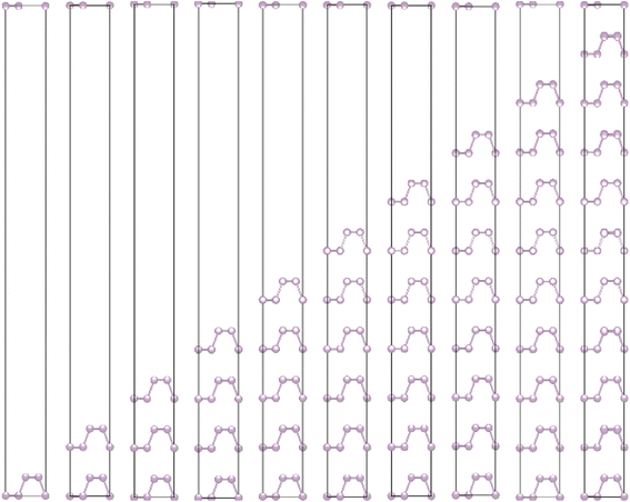
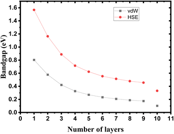
The crystalline structure of single and multilayer phosphorene is orthorhombic with a Cmca space group (N° 64) with lattice parameters a = 4.5257 Å and b = 3.2823 Å which are in good agreement with other reported data.35 Monolayer phosphorene contains two atomic layers bonded together by the SP3 hybridization of phosphorus atoms which caused the puckered honeycomb structure,36 the distance between two nearest atoms is 2.224 Å and the distance between top and bottom atoms is 2.244 Å. multilayer phosphorene are vertically stacked together with respect to one another by weak interlayer interaction named vdW forces (Fig. 1).37 The obtained electronic band structures (Fig. 2) show semiconductor nature with a direct band gap for exfoliated phosphorene and bulk phosphorene with 10L layers, where the calculated gap value for 1L (9L) is 1.57 eV (0.45 eV) and 0.80 eV (0.18 eV) with HSE and vdW, respectively (Fig. 3). The change in band gap is due to a loss of interlayer hybridization in exfoliated layer systems. Increasing the layer thickness leads to a down-shift of conduction band minimum (CBM) caused by the loss of interlayer hybridization between the stacked layers, giving a large anisotropic behavior of electronic structures with layer number. This anisotropic character of phosphorene results in highly anisotropic effective masses of electrons and holes (Fig. 4) in the respective directions (armchair or zigzag). The armchair direction (YY) presents the lower effective mass in contrast to the zigzag direction (XX). This, due to the difference in band dispersion along the YY and the XX direction. Furthermore, this effective mass anisotropy depends on the charge carrier. The holes in the XX direction present the highest effective mass whereas along the YY direction electrons are higher.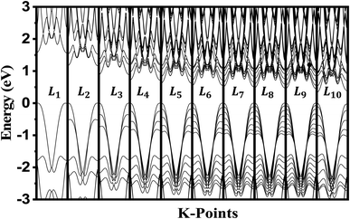 | ||
| Fig. 2 Electronic band structure dependence to phosphorene thickness. The Fermi level is shifted to 0 eV. | ||
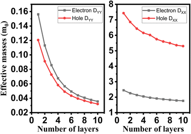 | ||
| Fig. 4 Layer engineering of holes and electrons effective mass in single and few layers phosphorene. | ||
Work function
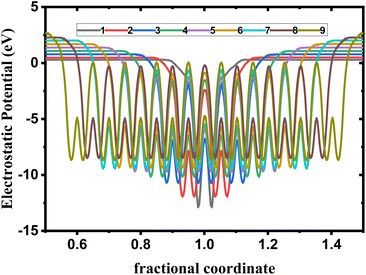
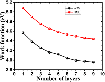
To ensure the feasibility of exfoliated phosphorene layers in optoelectronic and photonic applications, we analyze the work function as the energy needed for an electron emission to further understand the interaction between an emitted photon and excited electron in the studied surfaces. Numerous factors are used to control the work function, such as doping, strain, heterojunction, and layer number plays a key role in controlling the work function of phosphorene.We observe from Fig. 6 a sharp increase of the work function by decreasing the thickness of bulk phosphorene structure from 4.44 eV in 9L to 5.08 eV in 1L, and 3.96 eV in 9L to 4.57 eV in 1L for HSE and vdW, respectively. This remarkable changes in the work function with the thickness can be explained by the high confinement effect of electrons generated when the exfoliated layers are in 2D form, we suggest that when increasing the number of layers in phosphorene structure, the atoms in one layer become more closer to atoms in the second layer as a consequence of the decrease in the distance between layers due to the increase in the vdW interaction between layers. This leads to a higher vacuum potential energy which result to an increase in the electrostatic potential (Fig. 5).
Phonon and transport properties
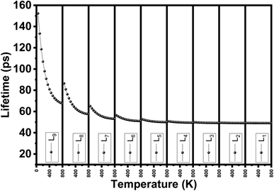
We evaluate the structural stability of the exfoliated phosphorene structures by calculating phonon dispersion along the high symmetry direction (Y-G-X-S). This, characterize the dynamic stability of the structures by evaluating the normal modes of the quantum vibrations, the criteria behind considering the crystal structure as stable require having only real frequencies in the phonon dispersion. The calculated phonon dispersion is presented in Fig. 7. In addition to temperature, or doping for tuning the phonon modes, our results show the possibility of engineering the phonon dispersion modes using vertical peeling of phosphorene layers. This is due to the changes in the chemical potential of the phosphorene 1L when adding other layers explained in the electronic properties from the calculated band structure. An insight into the phonon scattering mechanism in phosphorene is detailed to describe the effect of the exfoliated layers to adjust the phonon lifetime including temperature from 0 to 800 K. from our calculated phonon lifetime, it is seen that for all the exfoliated phosphorene structures, the phonon lifetime is shorter specially in monolayer phosphorene, this is due to the strong phonon scattering when reducing dimension. Increasing temperature is another factor that adjust the phonon lifetime, it is observed from Fig. 8 an increase in temperature is associated to a decrease in phonon lifetime. This is the result of an increase in the phonon interaction by the phonon thermal occupancy.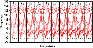 | ||
| Fig. 7 Phonon dispersion variation for exfoliated phosphorene layers from bulk phosphorene structure with 10 layers along Y-G-X-S direction. | ||
Optical properties
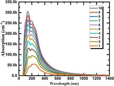
We calculate the optical absorption as a facile parameter in the optical properties and can be simple to carry out in experiments for phosphorene depended on layer thickness to explain the variation tendency of optical properties of phosphorene nanosheets obtained by exfoliation from the bulk structure and to provide a direct information to use for photovoltaic, photonic, and optoelectronic applications. As can be seen from Fig. 9 the aspect of the layer tunability of the optical absorption is phosphorene nanosheets is clearly observed. The absolute absorption intensity increased with a significant shift in wavelength when the layer thickness increase, this is essentially due to the strong interlayer couplings between layers provided by the strong exciton absorption and the decrease in the band gap energy value when reducing dimensionality. The continuum absorption observed in exfoliated 1L phosphorene which exhibits step-like features provide a typical character of 2D materials which is totally different from other dimensionalities and can be disappeared when increasing layer thickness.To develop the application performance for optoelectronics and photonics, non-equilibrium Green's function (NEGF) method was used to simulate the current–voltage dependent layer numbers. To perform the device, the system was divided into three different regions as presented in Fig. 10. The central channel region, the left electrode, and the right electrode, where a separate fully periodic calculation was the basis of the self-consistent Kohn–Sham potentials and the Hamiltonian of the electrodes. The system was treated as an open circuit, the reason where the Green's function was only solved in the central channel region.
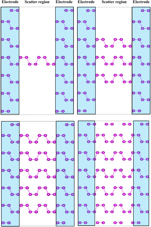 | ||
| Fig. 10 Schematic view of two-terminal left and right electrode regions (blue shade region) in contact with the central scattering region along the zigzag or armchair directions. | ||
As we know from the calculated band structures, phosphorene nanosheets is a p-type material. The reason to increase the contact resistance between the interfaces and to ensure the P–N junction, Ni-doped phosphorene was used in left and right electrodes, and it was confirmed using electronic band structure the transition from semi-conductor to conductor for Ni-doped phosphorene (Fig. 11). Furthermore, the current–voltage characteristic of phosphorene nanosheets systems as shown in Fig. 12 start to increase with increasing the applied voltages because of the semi-conducting behavior of 1, 3, 5, and 10 layers phosphorene. Apparently, it is observed that bulk phosphorene is more current sensitive than exfoliated phosphorene nanosheets. This can be attributed to the existence of a lower Schottky barrier at the interface of the bulk phosphorene with 10 layers as compared to that of phosphorene 1, 3 and 5 layers. This changes in the current sensitivity with the layer thickness opens the possible adjustment of I–V properties to be investigated in optoelectronic and photonic devices.
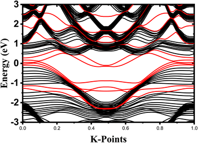 | ||
| Fig. 11 Electronic band structures of undoped one-layer phosphorene (black contribution) and Ni doped monolayer phosphorene (red contribution). The Fermi level is shifted to 0 eV. | ||
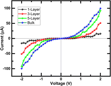 | ||
| Fig. 12 Current–voltage (I–V) characteristic of exfoliated 1, 3, 5 layers phosphorene from the bulk phosphorene structure with 10 layers under bias voltages from −2 V to +2 V. | ||
Conclusion
In this work, first principles method combined with non-equilibrium Green's function were been employed to investigate the possibility for tuning the optoelectronic and photonic properties with layer numbers in phosphorene. Anisotropic behavior was observed in the electronic and transport properties with a high dependence to the layer thickness for the band gap energy, carrier mobility, electrostatic potential, and I–V characteristic. The presence of positive frequency in the phonon spectrum gives the ground state dynamical stability of phosphorene dependent layer thickness. The computed optical properties reveal that the absorption spectrum show a decrease in intensity with a significant blue shift in wavelength when the exfoliated layer number decrease with a continuum absorption in 1L phosphorene characteristic of a single phosphorene sheet. More importantly, the I–V curve show the presence of a lower Schottky barrier at the interface of the bulk phosphorene as compared to that phosphorene nanosheets which result in a monotonical decrease in intensity when decreasing thickness. This sensitivity toward the layer thickness opens up the possibility for the engineering properties in phosphorene nanosheets to be investigated in optoelectronic and photonic devices.Conflicts of interest
The authors declare that they have no known competing financial interests or personal relationships that could have appeared to influence the work reported in this paper.Acknowledgements
The research leading to these results has received funding from OCP grant AS70 “Towards phosphorene-based materials and devices”.References
- K. S. Novoselov, A. K. Geim and S. V. Morozov, et al., Electric Field Effect in Atomically Thin Carbon Films, Science, 2004, 306(5696), 666–669, DOI:10.1126/science.1102896.
- M. Xu, T. Liang, M. Shi and H. Chen, Graphene-Like Two-Dimensional Materials, Chem. Rev., 2013, 113(5), 3766–3798, DOI:10.1021/cr300263a.
- Q. Tang, Z. Zhou and Z. Chen, Innovation and discovery of graphene-like materials via density-functional theory computations, Wiley Interdiscip. Rev. Comput. Mol. Sci., 2015, 5(5), 360–379, DOI:10.1002/wcms.1224.
- P. Ajayan, P. Kim and K. Banerjee, Two-dimensional van der Waals materials, Phys. Today, 2016, 69(9), 38–44, DOI:10.1063/PT.3.3297.
- R. Lv, J. A. Robinson and R. E. Schaak, et al., Transition Metal Dichalcogenides and Beyond: Synthesis, Properties, and Applications of Single- and Few-Layer Nanosheets, Acc. Chem. Res., 2015, 48(1), 56–64, DOI:10.1021/ar5002846.
- B. Liu, Transition Metal Dichalcogenides for High−Performance Aqueous Zinc Ion Batteries, Batteries, 2022, 8(7), 62, DOI:10.3390/batteries8070062.
- L. Song, L. Ci and H. Lu, et al., Large Scale Growth and Characterization of Atomic Hexagonal Boron Nitride Layers, Nano Lett., 2010, 10(8), 3209–3215, DOI:10.1021/nl1022139.
- A. Castellanos-Gomez, L. Vicarelli and E. Prada, et al., Isolation and Characterization of Few-Layer Black Phosphorus, 2D Mater., 2014, 1, 025001, DOI:10.1088/2053-1583/1/2/025001.
- L. Li, Y. Yu and G. J. Ye, et al., Black phosphorus field-effect transistors, Nat. Nanotechnol., 2014, 9(5), 372–377, DOI:10.1038/nnano.2014.35.
- F. Xia, H. Wang and Y. Jia, Rediscovering black phosphorus as an anisotropic layered material for optoelectronics and electronics, Nat. Commun., 2014, 5(1), 4458, DOI:10.1038/ncomms5458.
- V. Tran, R. Soklaski, Y. Liang and L. Yang, Layer-controlled band gap and anisotropic excitons in few-layer black phosphorus, Phys. Rev. B, 2014, 89(23), 235319, DOI:10.1103/PhysRevB.89.235319.
- J. Qiao, X. Kong, Z. X. Hu, F. Yang and W. Ji, High-mobility transport anisotropy and linear dichroism in few-layer black phosphorus, Nat. Commun., 2014, 5(1), 4475, DOI:10.1038/ncomms5475.
- J. Yoshinobu, Physical properties and chemical reactivity of the buckled dimer on Si(1 0 0), Prog. Surf. Sci., 2004, 77(1–2), 37–70, DOI:10.1016/j.progsurf.2004.07.001.
- A. Cupo and V. Meunier, Quantum confinement in black phosphorus-based nanostructures, J. Phys.: Condens. Matter, 2017, 29(28), 283001, DOI:10.1088/1361-648X/aa748c.
- M. Habiba, B. Abdelilah and E. K. Abdallah, et al., Enhanced photocatalytic activity of phosphorene under different pH values using density functional theory (DFT), RSC Adv., 2021, 11(26), 16004–16014, 10.1039/D0RA10246F.
- R. Fei and L. Yang, Strain-Engineering the Anisotropic Electrical Conductance of Few-Layer Black Phosphorus, Nano Lett., 2014, 14(5), 2884–2889, DOI:10.1021/nl500935z.
- M. Elahi, K. Khaliji, S. M. Tabatabaei, M. Pourfath and R. Asgari, Modulation of electronic and mechanical properties of phosphorene through strain, Phys. Rev. B, 2015, 91(11), 115412, DOI:10.1103/PhysRevB.91.115412.
- R. Fei, A. Faghaninia, R. Soklaski, J. A. Yan, C. Lo and L. Yang, Enhanced Thermoelectric Efficiency via Orthogonal Electrical and Thermal Conductances in Phosphorene, Nano Lett., 2014, 14(11), 6393–6399, DOI:10.1021/nl502865s.
- S. Das, W. Zhang, M. Demarteau, A. Hoffmann, M. Dubey and A. Roelofs, Tunable Transport Gap in Phosphorene, Nano Lett., 2014, 14(10), 5733–5739, DOI:10.1021/nl5025535.
- X. Peng, A. Copple and Q. Wei, Edge effects on the electronic properties of phosphorene nanoribbons, J. Appl. Phys., 2014, 116(14), 144301, DOI:10.1063/1.4897461.
- Y. Jing, Q. Tang, P. He, Z. Zhou and P. Shen, Small molecules make big differences: molecular doping effects on electronic and optical properties of phosphorene, Nanotechnology, 2015, 26(9), 095201, DOI:10.1088/0957-4484/26/9/095201.
- H. Mamori, A. El Kenz and A. Benyoussef, et al., Dynamic stability in phosphorene bilayer with different stacking orders: A first principle study, Mater. Sci. Semicond. Process., 2022, 140, 106341, DOI:10.1016/j.mssp.2021.106341.
- V. M. Bhagwat and B. V. Ramachandran, Malathion A and B esterases of mouse liver-I, Biochem. Pharmacol., 1975, 24(18), 1713–1717, DOI:10.1016/0006-2952(75)90011-8.
- J. P. Perdew, K. Burke and M. Ernzerhof, Generalized Gradient Approximation Made Simple, Phys. Rev. Lett., 1996, 77(18), 3865–3868, DOI:10.1103/PhysRevLett.77.3865.
- M. Dion, H. Rydberg, E. Schröder, D. C. Langreth and B. I. Lundqvist, Van der Waals Density Functional for General Geometries, Phys. Rev. Lett., 2004, 92(24), 246401, DOI:10.1103/PhysRevLett.92.246401.
- Z. Zhang, M. Q. Cheng and Q. Chen, et al., Monolayer Phosphorene–Carbon Nanotube Heterostructures for Photocatalysis: Analysis by Density Functional Theory, Nanoscale Res. Lett., 2019, 14(1), 233, DOI:10.1186/s11671-019-3066-z.
- J. M. Ziman and L. C. Luther, Principles of the Theory of Solids, Phys. Today, 1965, 18(2), 56, DOI:10.1063/1.3047187.
- Electron Transport in Compound Semiconductors, ed. B. Nag, Springer Berlin Heidelberg, 1980, vol. 11, DOI:10.1007/978-3-642-81416-7.
- T. J. Scheidemantel, C. Ambrosch-Draxl, T. Thonhauser, J. V. Badding and J. O. Sofo, Transport coefficients from first-principles calculations, Phys. Rev. B, 2003, 68(12), 125210, DOI:10.1103/PhysRevB.68.125210.
- F. Ricci, W. Chen and U. Aydemir, et al., An ab initio electronic transport database for inorganic materials, Sci. Data, 2017, 4(1), 170085, DOI:10.1038/sdata.2017.85.
- J. De Boor, On the applicability of the single parabolic band model to advanced thermoelectric materials with complex band structures, J. Materiomics, 2021, 7(3), 603–611, DOI:10.1016/j.jmat.2020.10.013.
- A. Kahn, Fermi level, work function and vacuum level, Mater. Horiz., 2016, 3(1), 7–10, 10.1039/C5MH00160A.
- M. Büttiker, Y. Imry, R. Landauer and S. Pinhas, Generalized many-channel conductance formula with application to small rings, Phys. Rev. B, 1985, 31(10), 6207–6215, DOI:10.1103/PhysRevB.31.6207.
- C. Guo, T. Wang, C. Xia and Y. Liu, Modulation of electronic transport properties in armchair phosphorene nanoribbons by doping and edge passivation, Sci. Rep., 2017, 7(1), 12799, DOI:10.1038/s41598-017-13212-7.
- M. Batmunkh, M. Bat-Erdene and J. G. Shapter, Phosphorene and Phosphorene-Based Materials - Prospects for Future Applications, Adv. Mater., 2016, 28(39), 8586–8617, DOI:10.1002/adma.201602254.
- A. S. Rodin, A. Carvalho and A. H. Castro Neto, Strain-Induced Gap Modification in Black Phosphorus, Phys. Rev. Lett., 2014, 112(17), 176801, DOI:10.1103/PhysRevLett.112.176801.
- S. Appalakondaiah, G. Vaitheeswaran, S. Lebègue, N. E. Christensen and A. Svane, Effect of van der Waals interactions on the structural and elastic properties of black phosphorus, Phys. Rev. B, 2012, 86(3), 035105, DOI:10.1103/PhysRevB.86.035105.
| This journal is © The Royal Society of Chemistry 2024 |


