 Open Access Article
Comprehensive study of nanostructured Bi2Te3 thermoelectric materials – insights from synchrotron radiation XRD, XAFS, and XRF techniques
N. G. Imamac,
Shaimaa Elyamny *b,
Giuliana Aquilanti
 c,
Simone Pollastri
 c,
Lara Gigli
 c and
Abd El-Hady B. Kashyout
 b
b
aExperimental Nuclear Physics Department (Solid State Laboratory), Nuclear Research Center (NRC), Egyptian Atomic Energy Authority (EAEA), Cairo 13759, Egypt
bElectronic Materials Research Department, Advanced Technology and New Materials Research Institute, City of Scientific Research and Technological Applications (SRTA-City), New Borg El-Arab City, P.O. Box 21934, Alexandria, Egypt. E-mail: selyamny@srtacity.sci.eg
cElettra – Sincrotrone Trieste, Strada Statale 14 – km 163,5 in AREA Science Park, Basovizza, 34149, Trieste, Italy
First published on 8th January 2024
Abstract
In this contribution, a comprehensive study of nanostructured Bi2Te3 (BT) thermoelectric material was performed using a combination of synchrotron radiation-based techniques such as XAFS, and XRF, along with some other laboratory techniques such as XRD, XPS, FESEM, and HRTEM. This study aims to track the change in morphological, compositional, average and local/electronic structures of Bi2Te3 of two different phases; nanostructure (thin film) and nanopowders (NPs). Bi2Te3 nanomaterial was fabricated as pellets using zone melting process in a one step process, while Bi2Te3 thin film was deposited on sodalime glass substrate using a vacuum thermal evaporation technique. Synchrotron radiation-based Bi LIII-edge fluorescence-mode X-ray absorption fine structure (XAFS) technique was performed to probe locally the electronic and fine structures of BT thin film around the Bi atom, while transmission-mode XAFS was used for BT NPs distributed in the PVP matrix. The structural features of the collected Bi LIII XANES spectra of thin film and powder samples of BT are compared with the simulated XANES spectrum of BT calculated using FDMNES code at 5 Å cluster size. Combining different off-line structural characterization techniques (XRD, FESEM, XPS, and HRTEM), along with those of synchrotron radiation-based techniques (XAFS and XRF) is necessary for complementary and supported average crystal, chemical, morphological and local electronic structural analyses for unveiling the variation between Bi2Te3 in the nanostructure/thin film and nanopowder morphology, and then connecting between the structural features and functions of BT in two different morphologies. After that, we measured the Seebeck coefficient and the power factor values for both the BT nanopowder and thin film.
1. Introduction
Around 60% of the total energy used in various industrial and processing operations is lost as waste heat.1 In order to fulfil peak carbon dioxide emissions and carbon neutrality targets, it is necessary to utilize clean and sustainable energy and the current energy conversion must become more efficient.2–4 Over 50% of all dissipated heat sources in industry come from low-grade heat. The consumption of fossil fuels can be reduced and the ensuing environmental crisis can be improved by low-grade heat recovery.1 The possibility of recovering low-temperature waste heat exists thanks to thermoelectric (TE) devices that can transform heat energy directly into electric energy.5–7 As well, it is a strategy that holds promise for resolving the contradiction between the rising energy demand and the depletion of fossil fuels2,8–10 by converting energy more sustainably utilising a noise-free, low-maintenance technique.11 Thermoelectric modules have frequently been used for thermal management.12 As a result, it is predicted that the global market for thermoelectric modules would grow to be worth US$ 1.3 billion by 2031 from its 2021 value of US$ 0.6 billion with growth rate 8.3%.13 The thermoelectric materials used in a thermoelectric device influence how efficient it is, therefore choosing a scalable, affordable TE material with great energy conversion capability is necessary.14,15 In general, the performance of thermoelectric materials, which is measured by the dimensionless figure of merit value, ZT determines the efficiency of thermoelectric devices.16 The thermoelectric qualities are assessed using the dimensionless figure of merit ZT = S2σT/K, where S, σ, T, and K, respectively, stand for the Seebeck coefficient, electrical conductivity, absolute temperature, and thermal conductivity.17 The preparation of materials with high electrical conductivity and low thermal conductivity, combined with a high value of the Seebeck coefficient, is the subject of several research projects, which can have a favourable figure of merit.18 Bismuth telluride (Bi2Te3) exhibits a remarkable thermoelectric performance close to room temperature (200–500 K) due to its inherently low lattice thermal conductivity, narrow gap, and high electronic mobility, which contributes to its large-scale applications.15,17,19 Because of the anisotropic transport properties of their layered structure, they provide fascinating case studies for electron/phonon transport.11 The thermoelectric performance will decrease as the temperature rises due to early intrinsic excitation.20 Room-temperature (RT) materials have made slow progress despite improvements in mid- and high temperature materials. For the past several decades, Bi2Te3-based alloys have remained the most advanced RT thermoelectric materials.12 This clearly shows the increased difficulty in achieving a high ZT at low temperatures, and in fact, materials like PbTe,21 Half-Heusler,22 SiGe,23 and GeTe24 have much improved ZT at mid-to-high temperatures. Bi2Te3-based alloys have long been the only high-performance thermoelectric materials available in the low-grade waste heat temperature range.25,26 Because thermoelectric thin film has the potential to be employed in the development of micropower generators in chip sensors for the internet of things (IoT), it has received a lot of attention.17 According to Zheng et al.27 who prepared a flexible Bi2Te3 thin film to be a suitable for use in wearable electronics as well as sensors. They found that there is still significant difficulty in connecting thermoelectric performance with flexibility. As well, Zheng and his co-authors28 observed that flexible thin films' weak thermoelectric performance restricts its application, indicating a significant need to enhance these characteristics. In the future, we planned to maintain the better thermoelectric performance of Bi2Te3 samples by transforming them into flexible films with a staggered-layer structure.Two main groups of synthesis procedures are used for chalcogenide TE compounds: (chemical) solution techniques and melting followed by pressing (physical). While solution methods have the advantage of allowing for the growth and control of various crystalline material architectures, they are only capable of producing a few grammes and cannot produce a high yield.11 Using solution synthesis techniques, the ZT for n-type Bi2Te3 could not be appreciably raised to values higher than 1.29,30 Particular procedures require a lot of time to prepare the necessary materials which associated costly facilities. The thermal evaporation method was used in this study to deposit Bi2Te3 thin films with improved thermoelectric features since it is an appealing technology and can provide some benefits, including simplicity, lower preparation costs, rapid processing, scalability to large areas, and high throughput.31
Thanks to the fascinating properties of synchrotron radiation (SR) which is currently widely used as a brilliant light source for studying deeply the structural features (morphological, compositional/chemical, average crystal, local/fine, etc.) of the matter.32–38 There are different beamlines-based techniques which were used for probing the BT thin film and BT nanopowders. Among them, SR-XAFS beamline at Elettra (Trieste-Italy) was used for collecting both the SR-XAFS and SR-XRF spectra.32 XRD technique is probing the average crystal structure and phase identification, while XAFS or X-ray absorption fine structure spectroscopy is an element-specific technique sensitive to probe the electronic and local structural properties over a variety of crystalline solid, semicrystalline, amorphous and/or glass, liquid or even gas substances. Generally, the solid sample can be in powder shape which should be pressed with a binder matrix to form a pellet having a thickness that meets the ideal signal-to-noise ratio, or in the form of bulk foil, or sheet, or bulk non-destructive sample or in thin film deposited layer on a substrate.39
The first region of the collected XAFS spectrum is called near-edge XAFS “XANES” and is among the most effective techniques for examining the electronic structure; symmetry and oxidation sates of absorbing atom within the investigated material. The tail region of the XAFS spectrum (>100 eV above the absorption edge and extends up to around 1000 eV after the edge value) is called extended XAFS “EXAFS” part where spectral oscillations is sensitive for the nature and coordination of the neighboring atoms surrounding the absorber element.
In our recent XAFS study40 we have studied Bi2Te3 and Sb doped Bi2Te3 (Bi2xSbxTe3) nanomaterials. XRD, Raman, SEM, and HRTEM, XAFS techniques and Laser-Beam Deflection Spectroscopy (BDS) were important techniques to fully investigate the samples nature, average crystal, morphological and local/electronic structures for unveiling the BiSbTe mechanism in thermoelectric generation. Also in that work, the effect of the Sb/Bi substitution on the fine/local structure was studied through the gradual elongation of the average in-plane Bi–Sb bond length.
Herein, this study represents a systematic completion of our published work on BT through distinguishing the differences of physical and chemical properties of BT in the case of thin film and powder morphology. Also, we established a reliable approach for the preparation of nanostructured Bi2Te3 thin film by combining zone melting and thermal evaporation processes in a high vacuum.
Moreover, this work is based on using of multitechnical approach through combining multi off-line structural characterization techniques, including powder X-ray diffraction (XRD), energy-dispersive X-ray (EDX), field emission scanning electron microscopy (FESEM), high-resolution transmission electron microscopy (HRTEM), and X-ray photoelectron spectroscopy (XPS), along with those of synchrotron radiation (SR) techniques, including SR-X-ray fluorescence spectrometer (XRF), and SR-X-ray Absorption Fine Structure Spectroscopy (XAFS). These techniques are necessary for complementary and supported average crystal, chemical, morphological and local electronic structural analyses to distinguish between Bi2Te3 nanostructure/thin film and nanopowders/pellet morphology and other physical properties.
2. Materials and methods
2.1. Bi2Te3 powder and thin film preparation
Bi2Te3 was synthesized from pure elements of Bi (Sigma Chemicals, 99.99%) and Te (Aldrich Chemicals, 99.999%) using a single step zone melting method.31,40 To preserve homogeneity and uniformity, the right amounts of these components were weighed using a digital balance and blended several times. After that, it was charged inside a 15 cm long, 0.8 cm wide, vacuum-sealed fused silica tubes. The tube was charged with precursors, evacuated to 3 × 10⁻³ mbar, then sealed with an oxygen flame to form a closed capsule. It was then melted at a temperature of 700 °C in a muffle furnace (Carbolite, CWF 1200), which was greater than the melting temperatures of Te (449.5 °C) and Bi (271.5 °C). The required reaction was successfully carried out by extending the melting period to 12 hours, and then cooled to room temperature in the furnace.41 This method for preparing the Bi2Te3 powder sample. Then, vacuum thermal evaporation was used to deposite Bi2Te3 thin films on substrates made of soda lime glass (Edwards Auto 306, USA). The substrates were cleaned using acetone, methanol, and distilled water in an ultrasonic bath before being dried under a stream of nitrogen. In order to prevent element contamination in a pressure of 10−6 mbar, the Bi2Te3 alloy was evaporated utilising heaters consisting of tungsten wire basket and quartz crucible.42 The substrate holders were rotated throughout the procedure of evaporation to guarantee the uniformity of the thin film structure and to produce homogeneous layers.2.2. Characterization techniques
The deposited thin film and the Bi2Te3 powder were studied for the structural and phase formation by the off-line laboratory powder X-ray diffraction (XRD) using Shimadzu 6100. CuKα radiation (λ = 1.54 Å) was used for the measurements of the powder's X-ray diffraction and it was produced at 40 kV and 30 mA. The scan was conducted in the 2θ ranges of 10° to 80° with a scanning rate of 12° min−1 at room temperature.An energy dispersive X-ray spectrometer (EDX) with a spectral range of 0 to 10 keV was applied to explain the bulk and thin film compositions. The incident electron beam was on two various locations of the sample in order to make sure it is homogeneous. To characterize the surface morphology and cross-sectional images of the surface of Bi2Te3 thin films, field emission scanning electron microscope (FESEM, Quanta 250 FEG) was used employing a 30 kV accelerating voltage and magnifications of 100![[thin space (1/6-em)]](https://www.rsc.org/images/entities/char_2009.gif) 000 and 40
000 and 40![[thin space (1/6-em)]](https://www.rsc.org/images/entities/char_2009.gif) 000, respectively.
000, respectively.
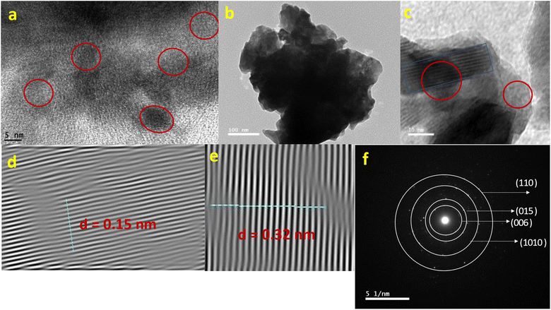
High-resolution transmission electron microscope (HR-TEM, JEOL-2100, Japan) was employed in conjunction with high resolution d-spacing of the various structures, electron diffraction and mapping of bismuth and tellurium elements to analyse the nano-morphology. To accomplish this, ethanol was added to a small portion of the sample. Following that, a copper grid that had been coated with carbon received a 10 μl application of the specimen for 30 seconds. After the excess liquid was removed using filter paper, the grid was dried in a desiccator. The PHI 5000 Versa Probe III Scanning XPS Microprobe with Monochromatic Al source ranging from 0–1486.6 eV was used for the X-ray Photoelectron Spectroscopy (XPS) measurement.
2.3. Thermoelectric analyses
The Hall Effect measurement system (MMR Technologies, Inc., 1400 North Shoreline Blvd., Unit A5, CA 94043) was used to examine the samples' resistivity by four probes at ambient temperature. To evaluate the Seebeck coefficient, the Bi2Te3 powder's output was ground and compressed into thin pellet that has thickness 1 mm and diameter 13 mm using a press machine (GrasebySpecac) at 450 MPa of pressure.40 Using a home-made setup, the Seebeck coefficient of the Bi2Te3 powder and thin film were estimated. Pt electrodes were sputtered on the sample surface at ambient temperature using the Hammer 8.1 sputtering technique (USA).312.4. Synchrotron radiation-based techniques
Bi LIII-edge XAS spectra of BT thin film were collected at XAFS beamline (ELETTRA, Trieste, Italy),43 in fluorescence mode using a silicon drift detector of 80 mm2 active area (AXAS-M, Ketek, Munich, Germany), and a fixed exit Si(111) monochromator. The XAFS spectra of BT powder and reference samples were measured in transmission mode using ionization chambers as the I0, I1, and I2 detectors. For all the samples, energy calibration was accomplished by collecting simultaneously a reference spectrum of Bi metal foil placed before I2 ionization chamber, with the energy position of the first inflection point taken at 13![[thin space (1/6-em)]](https://www.rsc.org/images/entities/char_2009.gif) 419.0 eV.
419.0 eV.
All spectra were collected at ambient temperature and in air with varying energy steps as a function of the energy: large step (5 eV) at the beginning 200 eV of the spectrum, smaller step (0.2 eV) in the XANES region and k-constant step of 0.03 Å−1 in the EXAFS region. Multiple spectra were collected and merged for both bulk and thin film of Bi2Te3 samples in order to increase the signal to noise ratio (2 spectra for transmission measurements and 6 for fluorescence ones). XAFS data were analyzed with the Demeter 0.9.26 software package.44 Whereas, the collected XAFS data were first processed in two spectral energy regions: analysis of near edge XAFS for electronic structure analysis and extended XAFS (EXAFS) region processing for atomic coordination and distance analysis.
Athena program (Demeter 0.9.26) was employed for XANES data processing and for extracting the EXAFS signal. The extracted EXAFS signal was fitted in Artemis program (Demeter 0.9.26) in order to extract the structural fitting parameters. In EXAFS fitting, Bi atom was selected as the photo absorber. The theoretical XANES spectra were calculated by FDMNES program45 and qualitatively compared with the XANES patterns collected from the XAFS experiment. Whereas, the cluster size of the electron wave function was changed until the spectra converged.45,46 The input file of FDMNES for the Bi2Te3 was built for a 3, 5, and 7 Å cluster size. The optimum cluster size for XANES calculation that fits well with the observed spectrum of Bi2Te3 is 5 Å.
Full XRF spectrum was also collected for Bi2Te3 thin film sample and on the glass substrate without any coating (blank measurement), with an incident beam energy of 17![[thin space (1/6-em)]](https://www.rsc.org/images/entities/char_2009.gif) 500 eV and roughly the same live time of 200 s. XAS data were analyzed with the Demeter 0.9.26 software package47 whereas XRF data were processed with PyMCA software.46
500 eV and roughly the same live time of 200 s. XAS data were analyzed with the Demeter 0.9.26 software package47 whereas XRF data were processed with PyMCA software.46
3. Results and discussions
3.1. Powder X-ray diffraction (XRD)
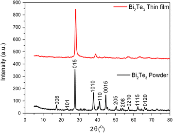
Bi2Te3 powder and thin film X-ray diffraction patterns were displayed in Fig. 1. It is demonstrated by the XRD patterns the fact that the specimens are polycrystalline in nature and belong to the rhombohedra crystal system based on the JCPDS card no. 008-0021. This indicates that the Bi2Te3 compound was effectively synthesized using the zone melting approach. All of the tested compounds have a single phase structure, are strongly orientated, and have the desirable orientation (015) plane at a 2θ angle of 27.7°. According to Y. Ma et al.,47 the desired crystal orientation is influenced by the composition of the sample. Furthermore, the other planes in the Bi2Te3 powder sample (006), (101), (1010), (110), (0015), (205), (208), (0210), (1115), and (1120), are represented by the main diffraction peaks at 2θ of 17.32°, 23.5°, 38°, 41.2°, 44.6°, 50.3°, 53.9°, 57.18°, 62.3° and 66.1°, respectively. Whiles, the Bi2Te3 thin film pattern presented fewer numbers of planes beside the preferred orientation (015). It includes the planes (1010), (0210) and (1115) at 2θ of 38°, 57.18° and 62.3°, respectively. Variations in these results are predicted. In general, a thin-film pattern does not need to have similar Bragg peaks as a powder; it just shows some peaks at similar peak positions. Grain orientation in powder measurements is always random, but in thin film, it is common referred as textured, indicating that the material has a preferred orientation in the direction of growth. As a consequence, they exhibit more prominent peaks on one lattice plane while the peak intensities of the others are significantly reduced or absent. From these data we noticed that the remarkable crystallinity of the Bi2Te3 powder and thin films was confirmed and the non-stoichiometric specimens were found to be free of additional phases.48 The primary peak's (015) broadness provides information about the particles' behavior that make up each sample at the nanometric scale. The crystallite size (t), as provided in eqn (1), is determined using Scherrer's formula:49
t = kλ/B![[thin space (1/6-em)]](https://www.rsc.org/images/entities/char_2009.gif) cos cos![[thin space (1/6-em)]](https://www.rsc.org/images/entities/char_2009.gif) θ θ
| (1) |
3.2. X-ray photoelectron spectroscopy (XPS)
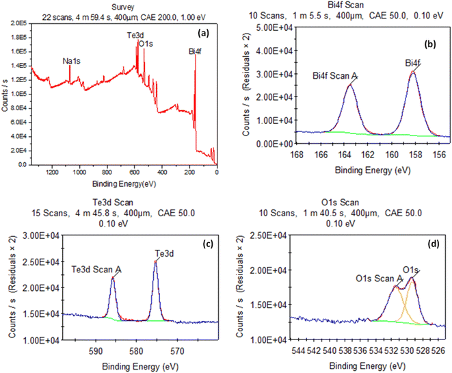
Fig. 2 shows the XPS measurements of the Bi2Te3 evaporated thin film. The survey wide scan spectrum is shown in Fig. 2(a). Te 3d with an atomic ratio of 35.84%, Bi 4f with an atomic ratio of 19.86%, O 1s with an atomic ratio of 32.06% and Na 1s with an atomic ratio of 12.24% are detected. Fig. 2(b–d), display the high-resolution spectra of Bi 4f, Te 3d5/2, and O 1s core levels, respectively. For Bi, there are two major peaks (Bi3+ 4f5/2 at BE = 158.2 eV with an atomic ratio of 57/01% and Bi3+ 4f7/2 at BE = 163.49 eV with an atomic ratio of 42.99%) as shown in Fig. 2(b) confirming the Bi2Te3 phase formation.41,42 The same is observed for Te with two major peaks at BE = 575.39 eV with an atomic ratio of 57.79% and the other one at BE = 585.76 eV with an atomic ratio, 42.21% Te2− 3d5/2 and Te2− 3d3/2 for the Bi2Te3 structure as shown in Fig. 2(c). The observed O 1s has two peaks observed at BE = 529.35 eV and 531.47 eV, which may be correspond to the surface oxidation in the Bi2Te3 phase which might occur as a result of being exposed to the atmosphere. This result is in agreement with Patil et al.51 who prepared Bi2(Te1−xSex)3 thin films doped by Sb. Also, there are no peaks detected either in XRD data or bismuth and tellurium oxides. Whiles, the presence of Na 1s may be duo to using Na-silicate glasses.523.3. Bi LIII-edge XANES spectral analyses & fitting
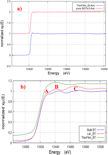
The collected Bi LIII-edge full normalized XAFS spectra of the structured thin film and powder samples of Bi2Te3 is shown in Fig. 3(a). While, FDMNES theoretically calculated XANES spectrum of Bi2Te3 is shown in Fig. 3(b), along with those of Bi2Te3 thin film and powder samples. Herein, the simulated calculated XANES spectrum of BT single phase was used to test/confirm the phase purity of BT either in case of thin film or powder sample.37Bi LIII-edge XANES region is arising from the excitation of the 2p3/2 electrons to the unoccupied 6d level of the Bi atoms.40 It is clear from Fig. 3(b) that the structural features labelled A, B, and C are missing in thin film spectrum indicating a structural difference of the thin film compared with the powder sample.
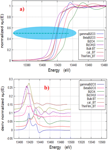
As reported in ref. 53, XANES spectrum of Bi LIII-edge is sensitive to the ionicity of Bi ions within the BT structure. Therefore, the edge energies of standard reference compounds of different Bi-compositions and structures (γ-Bi2O3, β-Bi2O3, Bi(OH)3, Bi2O4), are presented in Table 1 and shown in Fig. 4(a) together with the results obtained for the powder and thin film samples. Fig. 4(a) shows that the edge positions of powder and thin film samples are close to that of γ-Bi2O3 standard at 13![[thin space (1/6-em)]](https://www.rsc.org/images/entities/char_2009.gif) 419.3 ± 2 eV, indicating that the oxidation state of Bi ions in both Bi2Te3 thin film and powder samples is +3. For confirming the obtained oxidation state of Bi ions, the first derivative of the XANES spectra (dμ(E)/dE) for all samples and references are plotted as shown in Fig. 4(b). Accordingly, the same oxidation state of Bi is confirmed.
419.3 ± 2 eV, indicating that the oxidation state of Bi ions in both Bi2Te3 thin film and powder samples is +3. For confirming the obtained oxidation state of Bi ions, the first derivative of the XANES spectra (dμ(E)/dE) for all samples and references are plotted as shown in Fig. 4(b). Accordingly, the same oxidation state of Bi is confirmed.
| Sample | White-line position (eV) ± 0.2 | E0 (eV); selected at the half-height of the edge step ± 2 | Oxidation state of Bi |
|---|---|---|---|
| Bulk Bi2Te3 | 13![[thin space (1/6-em)]](https://www.rsc.org/images/entities/char_2009.gif) 444.81 444.81 |
13![[thin space (1/6-em)]](https://www.rsc.org/images/entities/char_2009.gif) 418.9 418.9 |
Bi3+ |
| Thin film Bi2Te3 | 13![[thin space (1/6-em)]](https://www.rsc.org/images/entities/char_2009.gif) 438.39 438.39 |
13![[thin space (1/6-em)]](https://www.rsc.org/images/entities/char_2009.gif) 418.7 418.7 |
Bi3+ |
| γ-Bi2O3 | 13![[thin space (1/6-em)]](https://www.rsc.org/images/entities/char_2009.gif) 436.6 436.6 |
13![[thin space (1/6-em)]](https://www.rsc.org/images/entities/char_2009.gif) 419.3 419.3 |
Bi3+ |
| β-Bi2O3 | 13![[thin space (1/6-em)]](https://www.rsc.org/images/entities/char_2009.gif) 447.0 447.0 |
13![[thin space (1/6-em)]](https://www.rsc.org/images/entities/char_2009.gif) 426.6 426.6 |
Bi3+ |
| Bi(OH)3 | 13![[thin space (1/6-em)]](https://www.rsc.org/images/entities/char_2009.gif) 440.49 440.49 |
13![[thin space (1/6-em)]](https://www.rsc.org/images/entities/char_2009.gif) 415.4 415.4 |
Bi3+ |
| Bi2O4 | 13![[thin space (1/6-em)]](https://www.rsc.org/images/entities/char_2009.gif) 452.6 452.6 |
13![[thin space (1/6-em)]](https://www.rsc.org/images/entities/char_2009.gif) 432.6 432.6 |
Bi4+ |
| Calculated Bi2Te3 | 13![[thin space (1/6-em)]](https://www.rsc.org/images/entities/char_2009.gif) 441.8 441.8 |
13![[thin space (1/6-em)]](https://www.rsc.org/images/entities/char_2009.gif) 419.4 419.4 |
Bi3+ |
Compared to XRD, XAFS is much more sensitive for tracking any slight change in the bond length or the relative atomic displacement. Therefore, Bi LIII-edge EXAFS fitting aims to determine the length of the ionic bonds of Bi–Te(Te1 & T2) and that of the covalent bonds of Bi–Bi inside BT structure of powder and thin film samples. According to the XAFS data quality, only the first coordination shell of Bi–Te(Te1 & T2) was fitted.
It is known that thin film is far from the structural equilibrium conditions compared to the powder material depending on the different growth conditions; as instance the composition of Bi/Te can be tuned by the growth temperature.54 The radial distribution function of the extracted EXAFS signal is plotted in Fig. 5(a and b) respectively as k2-weighted χ(R) for both Bi2Te3 thin film and powder samples. It is clear that the Fourier transform (FTs) spectrum of BT thin film is different compared to that of the powder sample. FTs of thin film sample is consisting of two FTs peaks at relatively shorter distance than those known for Bi–Te2.1/Te1.1 bonds. Most probably, these FTs peaks are concerning to Bi–O bonds. This result is matching well with that of XPS; that found two XPS peaks for oxygen and attributed that for the surface oxidation in the Bi2Te3 phase. Also, the formation of oxides may be due to the trapped oxygen into the crystallite site defects in the BT surface. Take into account there was not passivation layer on the top of the BT thin film.
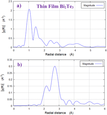 | ||
| Fig. 5 (a) Fourier transform of k2-weighted χ(R) of Bi2Te3 thin film, (b) Fourier transform of k2-weighted χ(R) of bulk Bi2Te3; at Bi LIII-edge. | ||
The fitted results of the EXAFS data enable a direct identification of the crystallite antisite defects in the Bi2Te3 thin film. Herein, the EXAFS signal was extracted by pre-analysis of the XAFS data in Athena program by removing/subtracting the XAFS background μ(E) and converting from μ(E) to χ(k). The Fourier transform (FTs) of k2-weighted EXAFS signal use Hanning windows with k-ranging from 2.1 to 10 Å−1, as plotted in Fig. 6. The fitted EXAFS results listed in Table 2 show that, at each Te site the Bi ion coordinates three Te ions for Bi–Te2.1 and Bi–Te1.1 bonds. The results in Table 2 match well with the schematic atomic coordination of Bi2Te3 described in Fig. 6(c).54 It is observed from Table 2 also that the bond lengths of Bi–Te2.1 of BT in the shape of thin film and powder are similar averaged at around 3.03 ± 0.13. While the bond length of Bi–Te1 of Bi2Te3 thin film is larger than that of powder Bi2Te3. It is clear also that there are differences in the radial distribution function of k2-weighted χ(R) between that of thin film and bulk Bi2Te3. These differences may be attributed to the formation of antistite defects in the thin film structure and the formation of oxide overgrown layer with time.55,56 The antistite defects or the disordering structure is confirmed from the higher values of the disorder parameter of the thin film compared to those of the bulk sample as shown from the EXAFS fitted results listed in Table 2.
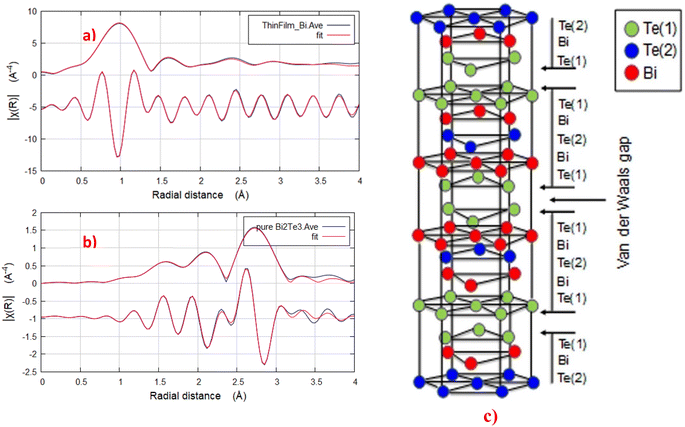 | ||
| Fig. 6 Bi LIII-edge k3 weighted experimental EXAFS data and the corresponding Artemis best fit for Bi2Te3 thin film and bulk samples; (a) and (b) respectively. (c) Schematic crystal structure of Bi2Te3.54 Fitting parameters: k-range = 2.2–10, dk = 0, k-window = Hanning, k-weight = 1, 2, 3, R-range = 2.2–4, dR = 0, R-window = Hanning, fitting space = r, background function = yes. | ||
| Path | N (atoms) | σ2 (Å2) ± 0.004 | R (Å) ± 0.13 |
|---|---|---|---|
| a S02 = 0.8, ΔE0 = −3.4 ± 0.02 eV, R-factor = 0.01. | |||
| Thin film Bi2Te3 | |||
| Bi–Te2.1 | 3 | 0.032 | 3.04 |
| Bi–Te1.1 | 3 | 0.031 | 3.76 |
| Bi–O1.1 | 4 | 0.022 | 2.63 |
![[thin space (1/6-em)]](https://www.rsc.org/images/entities/char_2009.gif) |
|||
| Bulk Bi2Te3 (powder) | |||
| Bi–Te2.1 | 3 | 0.013 | 3.02 |
| Bi–Te1.1 | 3 | 0.021 | 3.17 |
3.4. Synchrotron radiation based-XRF results
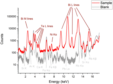
Fig. 7 shows a comparison of the XRF spectra collected on the thin film Bi2Te3 sample (red) and the glass substrate (grey). Brown labels represent the chemical elements attributable to the sample whereas grey ones are those attributable to the glass. As can be seen, the substrate glass contains (beyond obviously Si and Ca) an important fraction of Fe, Rb and Sr impurities whereas the Ar signal is due to the fact that measurements were conducted in air. However, in the XRF spectrum from the thin film sample, all the L fluorescence lines of both Te and Bi are clearly visible, with also a small signal from Ni, whereas all the other lines can be attributable to the substrate. Hence, we can exclude a contamination of the film sample from the chemical point of view.3.5. Morphological analysis
SEM and TEM are typically recognized as the two most extensively used techniques for examining nanoparticles. They were utilized to track the morphological configuration of the samples following the preparation of the Bi2Te3 powder and the deposition of the Bi2Te3 thin film. The right images explanation is essential because, despite certain commonalities, the analyses produced by the two approaches are not the same. Combining SEM and TEM enables the examination of surface area, form, dimensions, crystal structure, and morphological properties. SEM accurately captures the 3D surface and form details despite the fact that TEM equipment can offer noticeably higher 2D resolution for size analysis.![[thin space (1/6-em)]](https://www.rsc.org/images/entities/char_2009.gif) 000 and 50
000 and 50![[thin space (1/6-em)]](https://www.rsc.org/images/entities/char_2009.gif) 000). Whereas Fig. 8(c and d) represented the Bi2Te3 thin film surface images at magnification 100
000). Whereas Fig. 8(c and d) represented the Bi2Te3 thin film surface images at magnification 100![[thin space (1/6-em)]](https://www.rsc.org/images/entities/char_2009.gif) 000 and films' cross sections from the FESEM. The examined samples morphology revealed the crystalline nature and small grain sizes, which was supported by the XRD analyses. As shown in Fig. 8(a and b), the Bi2Te3 powder images demonstrate the closely packed grain edges in all samples, no preferential orientations, and a large number of delicate layered structures.40 The thickness of each layer is roughly 20 nm.40 This nanostructuration has a substantial impact on the samples thermoelectric properties, which leads to low heat conductivity in addition to high electrical conductivity. This is due to the numerous surface boundaries which are cause of large phonon scattering phenomena.40 As well, van der Waals gaps enable the Bi2Te3 powder sample to maintain laminar morphology and effectively realign its grains.40 Whereas in Fig. 8(c and d), the granular growth of Bi2Te3 thin films has exhibited irregular shape, with roughly 35 nm grain size and 1.9 nm thickness. Fig. 8(c) illustrates the absence of voids, unfilled spaces, or defects during the production of compact films, which are free of these imperfections.57 Additionally, grain formation happened primarily through the growth process rather than in a layer-by-layer approach, as shown by the FESEM images.39 From these results data, it is recommended that a more suitable and controlled procedure be used to create the Bi2Te3 composite using the zone melting method and depositing it using the thermal evaporation technique.
000 and films' cross sections from the FESEM. The examined samples morphology revealed the crystalline nature and small grain sizes, which was supported by the XRD analyses. As shown in Fig. 8(a and b), the Bi2Te3 powder images demonstrate the closely packed grain edges in all samples, no preferential orientations, and a large number of delicate layered structures.40 The thickness of each layer is roughly 20 nm.40 This nanostructuration has a substantial impact on the samples thermoelectric properties, which leads to low heat conductivity in addition to high electrical conductivity. This is due to the numerous surface boundaries which are cause of large phonon scattering phenomena.40 As well, van der Waals gaps enable the Bi2Te3 powder sample to maintain laminar morphology and effectively realign its grains.40 Whereas in Fig. 8(c and d), the granular growth of Bi2Te3 thin films has exhibited irregular shape, with roughly 35 nm grain size and 1.9 nm thickness. Fig. 8(c) illustrates the absence of voids, unfilled spaces, or defects during the production of compact films, which are free of these imperfections.57 Additionally, grain formation happened primarily through the growth process rather than in a layer-by-layer approach, as shown by the FESEM images.39 From these results data, it is recommended that a more suitable and controlled procedure be used to create the Bi2Te3 composite using the zone melting method and depositing it using the thermal evaporation technique.
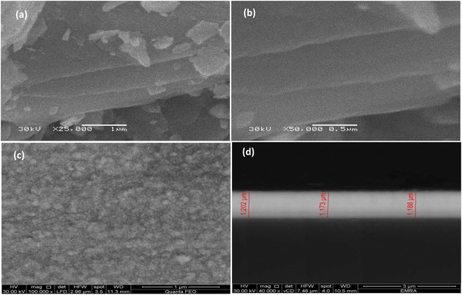 | ||
| Fig. 8 The FESEM of the Bi2Te3 powder at different magnifications (a and b), the morphological and cross-sectional images of Bi2Te3 thin film (c and d) respectively. | ||
Bi2Te3 powder and thin film stoichiometry were quantitatively examined using EDX analysis. The samples only consist of Bi and Te composition, according to the EDX examination, which also verifies that there are no other contaminants in the sample. The atomic% of Bi and Te in the Bi2Te3 thin film is found to be around 47.95 and 52.05, respectively. Whiles, the Bi and Te atomic% in the Bi2Te3 powder are discovered to be roughly 49 and 51, respectively.
3.6. Thermoelectric properties
A pair of thermocouple was positioned to the Bi2Te3 pellet and thin film samples on both sides at a spacing of 3 mm using two screws in order to measure the Seebeck coefficient. Because the directional migration of carriers in a conductor under a temperature gradient creates the Seebeck effect, a heater was used to raise the temperature of one side to roughly 230 °C. The Seebeck coefficient was determined using the following formula| S = ΔV/ΔT | (2) |
Next, we evaluated the electrical resistivity (ρ) of the powder and thin film Bi2Te3 at room temperature; the findings were approximately 1.8 × 10⁻⁴ and 1 × 10⁻⁴ (Ω m), respectively. Instead of ZT, thermoelectric devices' output power is directly correlated with their power factor (PF).61 In a consequence, we used eqn (3) to determine the thermoelectric power factor (PF) for both samples at room temperature and these approximately equaled for the pellet and thin film 78 and 400 μW K−2 m−1, respectively.
| PF = S2/ρ | (3) |
As compared with previous literature, the power factor value of the Bi2Te3 pellet in our work is higher than that measured by Ruamruk et al.62 They prepared a Bi2Te3 pellet by a hot press sintering process and found its power factor value equal to 62 μW K−2 m−1 at temperature 325 K. In addition, our power factor value of the Bi2Te3 thin film is greater than its value determined by Zang et al.63 which is around 200 μW K−2 m−1. This Bi2Te3 thin film was deposited by RF sputtering technique under 50 W power and at temperature 320 K.
As mentioned by Ashfaq et al.,64 at room temperature, the higher power factor value is a result of the lower electrical resistivity value and higher Seebeck coefficient.64 As a result, the power factor of the Bi2Te3 thin film is higher than that of the pellet. Moreover, they found that the surface morphology has also had an impact on the power factor values.64 As seen in the FESEM images, the Bi2Te3 thin film's grain size is smaller than those in the Bi2Te3 powder and the smaller grains provide more grain boundaries which enhances the Seebeck coefficient value as found by Ashfaq et al.64 As a consequence, it increases the power factor value in Bi2Te3 thin film.
4. Conclusions
In conclusion, we addressed a combined investigation of synchrotron radiation-based XAFS and XRF, along with XRD, XPS, FESEM, and HRTEM laboratory techniques to probe the evolution in the average, local, compositional, and morphological structural differences between structured Bi2Te3 thin film and Bi2Te3 in powdered form. Bi LIII-XANES spectra of the thin film clearly showed a different absorption feature rather than those of the powder and theoretically calculated XANES spectra. XANES results identified that the oxidation state of Bi ions in BT samples in both thin film and nanopowders phase were +3 and +3, respectively. The local structure of the NPs and thin film of Bi2Te3 was determined and distinguished with EXAFS fitting. XAFS and XPS agree together about the formation of two Bi–O bonds in BT thin film. The correlation between the coordination number of Bi–Te bonds via XAFS is clearly identified. Finally, by this contribution, we confirm that the physical properties of BT can be tuned without inserting chemical doping disorders via controlling the final shape of the prepared phase; powder or thin film. The characteristic structural variations between BT thin film and nanopowders form are consistent with physical properties and their functionality/applications. After that, we measured the Seebeck coefficient for Bi2Te3 bulk and thin film which were about −119 and −200 μV K−1, respectively. In addition, the thermoelectric power factors (PF) were determined to be 78 and 400 μW K−2 m−1 for both Bi2Te3 bulk and thin film, respectively.Author contributions
N. G. Imam: conceptualization, data curation, formal analysis, investigation, methodology, resources, software, supervision, validation, visualization, writing – original draft. Shaimaa Elyamny: conceptualization, data curation, formal analysis, investigation, methodology, resources, software, validation, visualization, writing – original draft, writing – review & editing. Giuliana Aquilanti: supervision. Simone Pollastri: methodology. Lara Gigli: methodology. Abd El-Hady B. Kashyout: conceptualization, data curation, formal analysis, supervision, validation, visualization, writing – original draft.Conflicts of interest
The authors declare no competing interests or non-financial interests.Acknowledgements
The XAFS, XRF, and XRD synchrotron experiments were performed during ICTP/Elettra TRIL fellowship of Neama Imam. The authors appreciate 11.1 XAFS and MCX beamlines at Elettra Synchrotron (Trieste, Italy). Many thanks to Jasper Rikkert PLAISIER (Head of MCX Beamline at Elettra). Also, ICTP, City of Scientific Research and Technological Applications (SRTA-City) and Egyptian Atomic Energy Authority (EAEA) are appreciated.References
- Z. Bu, X. Zhang, Y. Hu, Z. Chen, S. Lin, W. Li, C. Xiao and Y. Pei, A record thermoelectric efficiency in tellurium-free modules for low-grade waste heat recovery, Nat. Commun., 2022, 13, 237 CrossRef CAS PubMed.
- Q. Yan and M. G. Kanatzidis, High-performance thermoelectrics and challenges for practical devices, Nat. Mater., 2021, 21, 503–513 CrossRef PubMed.
- L. E. Bell, Cooling, heating, generating power, and recovering waste heat with thermoelectric systems, Science, 2008, 321, 1457–1461 CrossRef CAS PubMed.
- M. Liu, Y. Sun, J. Zhu, C. Li, F. Guo, Z. Liu, M. Guo, Y. Zhu, X. Dong, Z. Ge, Q. Zhang, W. Cai and J. Sui, High performance GeTe thermoelectrics enabled by lattice strain construction, Acta Mater., 2023, 244, 118565 CrossRef CAS.
- T. Zhu, Y. Liu, C. Fu, J. P. Heremans, J. G. Snyder and X. Zhao, Compromise and synergy in high-efficiency thermoelectric materials, Adv. Mater., 2017, 29, 1605884 CrossRef PubMed.
- S. Elyamny, E. Dimaggio, S. Magagna, D. Narducci and G. Pennelli, High power thermoelectric generator based on vertical silicon nanowires, Nano Lett., 2020, 20, 4748–4753 CrossRef CAS PubMed.
- S. Elyamny, E. Dimaggio and G. Pennelli, Seebeck coefficient of silicon nanowire forests doped by thermal diffusion, Beilstein J. Nanotechnol., 2020, 11, 1707–1713 CrossRef CAS PubMed.
- X. L. Shi, J. Zou and Z. G. Chen, Advanced thermoelectric design: from materials and structures to devices, Chem. Rev., 2020, 120, 7399–7515 CrossRef CAS PubMed.
- J. He and T. M. Tritt, Advances in thermoelectric materials research: looking back and moving forward, Science, 2017, 357, eaak9997 CrossRef PubMed.
- Y. Zheng, T. J. Slade, L. Hu, X. Y. Tan, Y. Luo, Z. Z. Luo, J. Xu, Q. Yan and M. G. Kanatzidis, Defect engineering in thermoelectric materials: what have we learned?, Chem. Soc. Rev., 2021, 50, 9022–9054 RSC.
- C. Gayner, L. T. Menezes, Y. Natanzon, Y. Kauffmann, H. Kleinke and Y. Amouyal, Development of Nanostructured Bi2Te3 with High Thermoelectric Performance by Scalable Synthesis and Microstructure Manipulations, ACS Appl. Mater. Interfaces, 2023, 15, 13012–13024 CrossRef CAS PubMed.
- J. Mao, H. Zhu, Z. Ding, Z. Liu, G. A. Gamage, G. Chen and Z. Ren, High thermoelectric cooling performance of n-type Mg3Bi2-based materials, Science, 2019, 365, 495–498 CrossRef CAS PubMed.
- Thermoelectric Modules Market, https://www.alliedmarketresearch.com/thermoelectric-modules-market-A13037, accessed January 2023.
- Z. Zheng, X. Shi, D. Ao, W. Liu, M. Li, L. Kou, Y. Chen, F. Li, M. Wei, G. Liang, P. Fan, G. Lu and Z. Chen, Harvesting waste heat with flexible Bi2Te3 thermoelectric thin film, Nat. Sustain., 2023, 6, 180–191 CrossRef.
- G. J. Snyder and E. S. Toberer, Complex Thermoelectric Materials, Nat. Mater., 2008, 7, 105–114 CrossRef CAS PubMed.
- J. Dong, Y. Jiang, J. Liu, J. Pei, X. Y. Tan, H. Hu, A. Suwardi, N. Jia, C. Liu, Q. Zhu, Q. Yan and J. Li, High thermoelectric performance in GeTe with compositional insensitivity, Nano Energy, 2022, 103, 107809 CrossRef CAS.
- Y. Chen, J. Zhang, M. Nisar, A. Abbas, F. Li, G. Liang, P. Fan and Z. Zheng, Realizing high thermoelectric performance in n-type Bi2Te3 based thin films via post-selenization diffusion, J Mater., 2023, 9, 618–625 Search PubMed.
- G. Pennelli, S. Elyamny and E. Dimaggio, Thermal conductivity of silicon nanowire forests, Nanotechnology, 2018, 29, 505402 CrossRef CAS PubMed.
- H. Soliman and A. Kashyout, Electrochemical deposition and optimization of thermoelectric nanostructured bismuth telluride thick films, Engineering, 2011, 3, 659–667 CrossRef CAS.
- Y. Sun, H. Qin, C. Zhang, H. Wu, L. Yin, Z. Liu, S. Guo, Q. Zhang, W. Cai, H. Wu, F. Guo and J. Sui, Sb2Te3 based alloy with high thermoelectric and mechanical performance for low-temperature energy harvesting, Nano Energy, 2023, 107, 108176 CrossRef CAS.
- P. Jood, M. Ohta, A. Yamamoto and M. G. Kanatzidis, Excessively Doped PbTe with Ge-Induced Nanostructures Enables High-Efficiency Thermoelectric Modules, Joule, 2018, 2, 1339–1355 CrossRef CAS.
- J. Yu, Y. Xing, C. Hu, Z. Huang, Q. Qiu, C. Wang, K. Xia, Z. Wang, S. Bai, X. Zhao, L. Chen and T. Zhu, Half-Heusler Thermoelectric Module with High Conversion Efficiency and High Power Density, Adv. Energy Mater., 2020, 10, 2000888 CrossRef CAS.
- S. Ahmad, A. Singh, A. Bohra, R. Basu, S. Bhattacharya, R. Bhatt, K. N. Meshram, M. Roy, S. K. Sarkar, Y. Hayakawa, A. K. Debnath, D. K. Aswal and S. K. Gupta, Boosting thermoelectric performance of p-type SiGe alloys through in-situ metallic YSi2 nanoinclusions, Nano Energy, 2016, 27, 282–297 CrossRef CAS.
- Z. Liu, W. Gao, W. Zhang, N. Sato, Q. Guo and T. Mori, High Power Factor and Enhanced Thermoelectric Performance in Sc and Bi Codoped GeTe: Insights into the Hidden Role of Rhombohedral Distortion Degree, Adv. Energy Mater., 2020, 10, 2002588 CrossRef CAS.
- F. Hao, P. Qiu, Y. Tang, S. Bai, T. Xing, H. Chu, Q. Zhang, P. Lu, T. Zhang, D. Ren, J. Chen, X. Shi and L. Chen, High efficiency Bi2Te3-based materials and devices for thermoelectric power generation between 100 and 300 °C, Energy Environ. Sci., 2016, 9, 3120–3127 RSC.
- B. Zhu, X. Liu, Q. Wang, Y. Qiu, Z. Shu, Z. Guo, Y. Tong, J. Cui, M. Guc and J. He, Realizing record high performance in n-type Bi2Te3-based thermoelectric materials, Energy Environ. Sci., 2020, 13, 2106–2114 RSC.
- Z. Zheng, X. Shi, D. Ao, W. Liu, M. Li, L. Kou, Y. Chen, F. Li, M. Wei, G. Liang, P. Fan, G. Lu and Z. Chen, Harvesting waste heat with flexible Bi2Te3 thermoelectric thin film, Nat. Sustain., 2023, 6, 180–191 CrossRef.
- Z. Zheng, Y. Li, J. Niu, M. Wei, D. Zhang, Y. Zhong, M. Nisar, A. Abbas, S. Chen, F. Li, G. Liang, P. Fana and Y. Chen, Significantly (00l)-textured Ag2Se thin films with excellent thermoelectric performance for flexible power applications, J. Mater. Chem. A, 2022, 10, 21603–21610 RSC.
- J. Fu, S. Song, X. Zhang, F. Cao, L. Zhou, X. Li and H. Zhang, Bi2Te3 Nanoplates and Nanoflowers: Synthesized by Hydrothermal Process and Their Enhanced Thermoelectric Properties, CrystEngComm, 2012, 14, 2159–2165 RSC.
- R. J. Mehta, Y. Zhang, C. Karthik, B. Singh, R. W. Siegel, T. Tasciuc and G. Ramanath, A New Class of Doped Nanobulk High-Figure-of-Merit Thermoelectrics by Scalable Bottom-up Assembly, Nat. Mater., 2012, 11, 233–240 CrossRef CAS.
- S. Elyamny and A. B. Kashyout, Preparation and Characterization of The Nanostructured Bismuth Telluride Thin Films Deposited by Thermal Evaporation Technique, Mater. Today: Proc., 2019, 8, 680–689 CAS.
- M. Monged, N. Imam, G. Aquilanti, S. Pollastri, A. Rashad and J. Osan, Heavy metals concentrations and speciation of Pb and Ni in airborne particulate matter over two residential sites in Greater Cairo – reflection from synchrotron radiation, J. Synchrotron Radiat., 2022, 29, 765 CrossRef CAS.
- M. M. Arman, N. G. Imam, R. L. Portales and S. I. El-Dek, Synchrotron radiation X-ray absorption fine structure and magnetization improvement of A-site Ce3+ doped LaFeO3, J. Magn. Magn. Mater., 2021, 513, 167097 CrossRef.
- N. G. Imam, G. Aquilanti, A. A. Azab and S. E. Ali, Correlation between structural asymmetry and magnetization in Bi-doped LaFeO3 perovskite: a combined XRD and synchrotron radiation XAS study, Mater. Sci.: Mater. Electron., 2021, 32, 3361–3376 CAS.
- N. G. Imam, M. AbouHasswa and N. Okasha, Synchrotron X-ray absorption fine structure study and dielectric performance of Li0.5Fe2.5O4/BaTiO3 multiferroic, Mater. Sci.: Mater. Electron., 2021, 32, 21492–21510 CAS.
- N. G. Imam, M. AbouHasswa, A. I. Ali and N. Okasha, Optimization of magnetic properties of BaTiO3/Li0. 5Fe2.5O4 multiferroics prepared via modified low-temperature combustion, Mater. Sci.: Mater. Electron., 2022, 33, 7945–7959 CAS.
- N. G. Imam, M. AbouHasswa, G. Aquilanti, S. I. El Dek, N. Okasha and A. A. G. Al Shahawy, Influence of polyethylene glycol on the physical properties of Co0.2Fe2.8O4 nanoparticles used as MRI contrast agent; synchrotron radiation Fe K-edge XAFS, J. Mater. Res. Technol., 2021, 15, 4130–4146 CrossRef CAS.
- N. G. Imam, M. Harfouche, A. A. Azab and S. Solyman, Coupling between γ-irradiation and synchrotron-radiation-based XAFS techniques for studying Mn-doped ZnO nanoparticles, J. Synchrotron Radiat., 2022, 29, 1187 CrossRef CAS PubMed.
- T. Liu, Y. N. Xie and T. D. Hu, An XAFS measurement of copper thin film by a simple detector in total-electron-yield mode, Nucl. Instrum. Methods Phys. Res., Sect. B, 2000, 160, 301–306 CrossRef CAS.
- S. Elyamny, N. G. Imam, G. Aquilanti, H. Cabrera and A. B. Kashyout, Thermal transport properties for unveiling the mechanism of BiSbTe alloys in thermoelectric generation: A glance from synchrotron radiation Bi L3-XAFS, J. Mater. Res. Technol., 2022, 18, 2261–2272 CrossRef CAS.
- M. Ahmad, K. Agarwal and B. R. Mehta, An anomalously high Seebeck coefficient and power factor in ultrathin Bi2Te3 film: Spin–orbit interaction, J. Appl. Phys., 2020, 128, 035108 CrossRef CAS.
- C. Hsiao and Y. Wu, Fabrication of flexible thin-film thermoelectric generators, J. Chin. Inst. Eng., 2011, 34, 809–816 CrossRef CAS.
- A. Cicco, G. Aquilanti, M. Minicucci, E. Principi, N. Novello, A. Cognigni and L. Olivi, Novel XAFS capabilities at ELETTRA synchrotron light source, J. Phys.: Conf. Ser., 2009, 190, 012043 CrossRef.
- B. Ravel and M. Newville, ATHENA, ARTEMIS, HEPHAESTUS: data analysis for X-ray absorption spectroscopy using IFEFFIT, J. Synchrotron Radiat., 2005, 12, 537 CrossRef CAS PubMed.
- V. A. Solé, E. Papillon, M. Cotte, P. Walter and J. A. Susini, A multiplatform code for the analysis of energy-dispersive X-ray fluorescence spectra, Spectrochim. Acta, Part B, 2007, 62, 63–68 CrossRef.
- J. Jutimoosik, P. Kidkhunthod, T. Bongkarn and R. Yimnirun, Local structure and cation distribution analysis of Mn1-xZnxFe2O4 powders by X-ray Absorption Near Edge Structure spectroscopy, Radiat. Phys. Chem., 2021, 188, 109628 CrossRef CAS.
- Y. Ma, E. Ahlberg, Y. Sun, B. Iversen and A. E. C. Palmqvist, Thermoelectric properties of thin films of bismuth telluride electrochemically deposited on stainless steel substrates, Electrochim. Acta, 2011, 56, 4216–4223 CrossRef CAS.
- J. S. Khan, R. Akram, A. A. Shah, M. Hussain, S. Rafique, A. Rehman, T. Khurshid and K. Karim, Enhanced zT due to non-stoichiometric induced defects for bismuth telluride thermoelectric materials, Kuwait J. Sci., 2023, 50, 231–237 CrossRef.
- B. D. Cullity, Elements of X-Ray Diffraction, Addison-Wesley Publishing Company Inc., U.S.A., 2nd edn, 1978 Search PubMed.
- F. Yu, J. Zhang, D. Yu, J. He, Z. Liu, B. Xu and Y. Tian, Enhanced thermoelectric figure of merit in nanocrystalline Bi2Te3 bulk, J. Appl. Phys., 2009, 105, 094303 CrossRef.
- S. M. Patil, S. N. Gavale, R. K. Mane, N. S. Patil, S. S. Mali, P. S. Patil and P. N. Bhosale, XPS characterization and opto structural study of chemically deposited Sb (III) doped Bi2(Te1-xSex)3 thin films, Arch. Phys. Res., 2012, 3, 245–257 CAS.
- G. Pintori and E. Cattaruzza, XPS/ESCA on glass surfaces: A useful tool for ancient and modern materials, Opt. Mater.: X, 2022, 13, 100108 CAS.
- N. Jiang and J. C. H. Spence, Can near-edge structure of the Bi L3 edge determine the formal valence states of Bi?, J. Phys.: Condens. Matter, 2006, 18, 8029 CrossRef CAS.
- Y. Hosokawa, K. Tomita and M. Takashiri, Growth of single-crystalline Bi2Te3 hexagonal nanoplates with and without single nanopores during temperature-controlled solvothermal synthesis, Sci. Rep., 2019, 9, 10790 CrossRef.
- P. Chuang, S. Su, C. Chong, Y. Chen, Y. Chou, J. Huang, W. Chen, C. Cheng, K. Tsuei, C. Wang, Y. Yang, Y. Liao, S. Weng, J. Lee, Y. Lan, S. Chang, C. Lee, C. Yang, H. Su and Y. Wu, Anti-site defect effect on the electronic structure of a Bi2Te3 topological insulator, RSC Adv., 2018, 8, 423–428 RSC.
- X. Hong, M. Newville, Y. Ding, D. Zhang, T. Irifune, G. Gu and H. Mao, Origin of the isostructural electronic states of the topological insulator Bi2Te3, Phys. Rev. B, 2020, 102, 134110 CrossRef CAS.
- A. M. Adam, E. Lilov and P. Petkov, Optical and thermoelectric properties of nano-particles based Bi2(Te1−xSex)3 thin films, Superlattices Microstruct., 2017, 101, 609–624 CrossRef CAS.
- Y. Liu, M. Zhou and J. He, Towards higher thermoelectric performance of Bi2Te3 via defect engineering, Scr. Mater., 2016, 111, 39–43 CrossRef CAS.
- R. Cao, Z. Zhu, X. Li, X. Hu and H. Song, Enhanced thermoelectric properties of the Lu-doped and CNT-dispersed Bi2Te3 alloy, Appl. Phys. A, 2019, 125, 126 CrossRef.
- V. S. Khairnar, A. N. Kulkarni, V. V. Lonikar, A. B. Gite, M. Kumar, D. P. Patil and D. P. Kadam, Electrodeposition of Bi2Te3 thin films for thermoelectric applications: effect of electrolyte pH, J. Mater. Sci.: Mater. Electron., 2023, 34, 875 CrossRef CAS.
- J. Cha, C. Zhou, S. Cho, S. H. Park and I. Chung, Ultrahigh Power Factor and Electron Mobility in n-Type Bi2Te3–x%Cu Stabilized under Excess Te Condition, ACS Appl. Mater. Interfaces, 2019, 11, 30999–31008 CrossRef CAS PubMed.
- S. Ruamruk, B. Chayasombat, K. Singsoog, A. Vora-ud, W. Namhongsa, P. Pilasuta and T. Seetawan, power factor of Bi2Te3 and Sb2Te3 enhanced by high density and hardness, Suranaree J. Sci. Technol., 2023, 30(1–5), 030145 Search PubMed.
- K. -Y. Zang, E. -T. Hu, Z. -Y. Wang, H. -T. Tu, Y. -X. Zheng, S. -Y. Wang, H. -B. Zhao, Y. -M. Yang, Y. -P. Lee and L. -Y. Chen, Effect of deposition power on the thermoelectric performance of Bismuth Telluride prepared by RF sputtering, Crystals, 2020, 10, 552 CrossRef CAS.
- A. Ashfaq, M. M. Sabugaa, M. B. Moussa, N. Almousa, E. A. Shokralla, R. Y. Capangpangan, A. C. Alguno, M. A. Hossain, A. M. Alanazi and M. Abboud, High thermoelectric power factor of Sr doped Bi2Te3 thin film through energy filtering effect, Int. Commun. Heat Mass Transfer, 2023, 143, 106719 CrossRef CAS.
| This journal is © The Royal Society of Chemistry 2024 |

