 Open Access Article
The effect of morphology and crystal structure on the photocatalytic and photoelectrochemical performances of WO3†
Lihua Li*a,
Jingjing Lib,
BoK.-Hee Kimac and
Jinliang Huang a
a
aSchool of Materials Science and Engineering, Henan University of Science and Technology, Luoyang 471023, China. E-mail: lilihua7818@163.com
bSchool of Materials Science and Engineering, Luoyang Institute of Science and Technology, Luoyang 471023, China
cDivision of Advanced Materials Engineering, Hydrogen and Fuel Cell Research Center, Chonbuk National University, Jeonju 561-756, South Korea
First published on 9th January 2024
Abstract
A template-based solvothermal method was successfully developed for the controlled synthesis of two-dimensional (2D) monoclinic WO3 nanoplate/nanosheet arrays and three-dimensional (3D) hexagonal WO3 nanosphere/nanocage structures with single crystal petals. The structure-directing agents played an important role in controlling the morphology and phase of WO3 samples. The results showed that the WO3 nanospheres exhibited the highest visible light absorption capacity and a photocurrent density of 0.37 mA cm−2 at 1.23 V vs. RHE under simulated sunlight. Moreover, the photocatalytic dye results displayed 83.2% methylene blue degradation and 87.9% rhodamine B degradation within 120 min under visible light irradiation. The high performance of the WO3 nanospheres, resulted from the hierarchical structure, increased surface area and enhanced light absorption, which improved the photogenerated charge carrier transfer and separation capability.
1. Introduction
Tungsten trioxide (WO3) is an n-type indirect band gap semiconductor material with a band gap of 2.5–2.8 eV, which can absorb approximately 12% of the solar spectrum.1,2 Moreover, WO3 has good electron mobility, suitable hole diffusion length, and good chemical stability in acid solutions, and it has been widely used in photocatalysis and photoelectrochemical fields.3–5 It is well known that the photocatalytic and photoelectrochemical performances of WO3 are closely related to its morphology and structure. Zhou et al.6 synthesized WO3 with seed-like, nanoflake and nanorod array morphologies on FTO substrates via a moderate hydrothermal approach; the WO3 nanoplate arrays exhibited excellent photocurrent density and MO degradation activities. Farhadian et al.7 prepared WO3 nanorods, nanospheres and nanoplates using a hydrothermal method; the results showed that WO3 nanoplates had an efficient photocatalytic degradation activity for rhodamine B. Li et al.8 synthesized amorphous, cubic and monoclinic WO3 films through a solution-based method by varying the annealing temperature; the WO3 film annealed at 450 °C presented significant photoanodic current. Szilágyi et al.9 prepared monoclinic and hexagonal WO3 nanoparticles by annealing (NH4)xWO3−y, and the oxidized monoclinic WO3 displayed the highest photocatalytic activity both in the gas and the liquid phases.Drawing from the abovementioned literature,10,11 the WO3 suspended powder is the most investigated substance in the area of photocatalysis, while the object of the photoelectrochemical system was WO3 thin film electrodes. WO3 nanostructures with different morphologies or crystal phases exhibit different catalytic activities in photocatalytic or photoelectrochemical systems.12 However, there are few reports on the photocatalytic and photoelectrochemical properties of WO3 films with various morphologies and crystal phases. Two-dimensional (2D) and three-dimensional (3D) WO3 films have been widely investigated because of their large exposed surface area and enhanced light scattering and absorption.13,14 At present, research on the properties of WO3 mainly focuses on the study of the monoclinic phase, and there are few studies on the hexagonal phase. In addition, the differences in photocatalytic and photoelectrochemical performances between 2D (3D) morphologies and crystal structures are not yet known.
In this study, 2D monoclinic WO3 arrays and 3D hierarchical hexagonal WO3 films were successfully synthesized using a solvothermal method by adjusting the morphology control agent. The growth mechanism of WO3 under different reaction conditions was analysed. The photocatalytic performance of the obtained WO3 films was investigated based on the degradation of methylene blue (MB) and rhodamine B (RhB) under visible light. The effect of the morphology and crystal structure value on photocatalytic and photoelectrochemical performance is discussed. The crystal structures and densities of states were determined using first-principles calculations.
2. Experimental sections
2.1 Materials
Chemical reagents such as sodium tungsten dehydrate (Na2WO4·2H2O), hydrochloric acid (HCl, 36–38%), oxalate (H2C2O4·2H2O), citrate (C6H8O7·H2O), acetonitrile (CH3CN), hydrogen peroxide H2O2 (30%), acetone (CH3COCH3), and ethanol absolute were used as starting reagents. All chemical reagents were analytical grade and used without further purification. All aqueous solutions were prepared using deionized water. Glass substrates coated with fluorine-doped tin oxide (FTO) were cut into slides of size 1 cm × 5 cm and cleaned sequentially with acetone, absolute ethanol, and deionized water in an ultrasonic bath (Nanjing Kenyan electronic technology Co. Ltd., KF-C27) each for 20 min and dried for the reserve.2.2 Experimental
The fabrication process of 2D arrays: 0.6597 g of Na2WO4·2H2O was dissolved in 35 mL deionized water, then 2 mL of hydrochloric acid was added under stirring for 10 min. Subsequently, 0.2 g of oxalate or citric was added followed by magnetic stirring for 30 min. Then, 20 mL of the mixed solution was transferred into a 50 mL Teflon-lined autoclave in which the FTO substrate was placed at an angle against the wall of the Teflon liner with the conductive surface facing down. Hydrothermal synthesis was conducted at 120 °C for 12 h. After the reaction, the autoclave was cooled naturally to room temperature, washed with deionized water and ethanol 3 times to remove ions that may have remained in the final products, and dried at 60 °C for 8 h in air. Finally, the obtained samples were annealed at 450 °C in the air for 1 h at a heating rate of 2 °C min−1.The fabrication process of 3D hierarchical films: 0.6597 g of Na2WO4·2H2O was dissolved in a mixture of acetone (acetonitrile) and deionized water with a volume ratio of 2![[thin space (1/6-em)]](https://www.rsc.org/images/entities/char_2009.gif) :
:![[thin space (1/6-em)]](https://www.rsc.org/images/entities/char_2009.gif) 5, the remaining steps were the same as those stated above.
5, the remaining steps were the same as those stated above.
2.3 Characterization
The crystal structure was characterized by X-ray diffraction (XRD, Bruker D8, Cu Kα radiation). The morphologies of the samples were observed on a scanning electron microscope (SEM, JSM-IT100, Japan), transmission electron microscopy (TEM), and high-resolution TEM (HRTEM) were performed on a Titan G2 60-300 instrument with an accelerating voltage of 200 kV. Optical absorption spectra were measured using ultraviolet-visible spectroscopy (UV-vis, UV-2600, Japan). Room temperature photoluminescence (PL, F-280, Tianjin) spectra were measured using a 325 nm continuous wave laser as the exciting source.2.4 Photoelectrochemical measurements
The photoelectrochemical performance of WO3 was evaluated in typical three-electrode cells with a platinum foil as a counter electrode and saturated Ag/AgCl as the reference electrode using the CHI 660e electrochemical workstation. The WO3 electrode with a tested area of 1 cm2 was used as a working electrode. 0.5 M Na2SO4 solution was used as an electrolyte for the PEC test. The light source was an Xe 300 W Xe arc lamp (CEL-S500) with an AM 1.5G filter (about 100 mW cm−2). The measured potentials vs. Ag/AgCl were converted to the potentials vs. the reversible hydrogen electrode (RHE) using the Nernst equation:15| ERHE = EAg/AgCl + 0.059 pH + EAg/AgCl0 |
Linear sweep voltammetry (LSV) was monitored with a scan rate of 10 mV s−1. The electrochemical impedance spectroscope (EIS) was conducted at an open potential, with a sinusoidal ac perturbation of 10 mV applied over a frequency range of 100 kHz to 0.01 Hz. Mott–Schottky (M–S) analysis was performed using an AC potential frequency of 10 kHz under dark conditions.
2.5 Photocatalytic degradation experiment
The photocatalytic activities of WO3 films were evaluated through the degradation of MB and RhB solutions at an initial concentration of 10 mg L−1. The WO3 film photocatalyst was vertically placed in the solution. Before irradiation, the solution was magnetically stirred under dark conditions for 30 min to establish an adsorption–desorption equilibrium.16 The lamp was switched on, and 3 mL of the reaction solution was taken every 20 min, and the concentration was measured using the UV-vis spectrophotometer.2.6 Computational details
First-principles calculations based on density functional theory (DFT) were performed to analyze the crystal structure and density of states (DOS) of WO3. The Perdew–Burke–Ernzerhof (PBE) method based on the generalized gradient approximation (GGA) was employed for the exchange–correlation function. The valence electron–ion interactions were substituted by ultra-soft pseudopotential. The cutoff energy was set to 400 eV for a plane-wave basis and the k-point mesh was taken as 4 × 4 × 4 for the bulk calculations. The Broyden–Fletcher–Goldfarb–Shanno (BFGS) algorithm was used for the optimization. The convergence criteria for energy, maximum force, maximum stress, and maximum displacement were set as 10−5 eV atom−1, 0.03 eV Å−1, 0.05 GPa, and 0.001 Å, respectively.3. Results and discussion
3.1 Morphology and structure
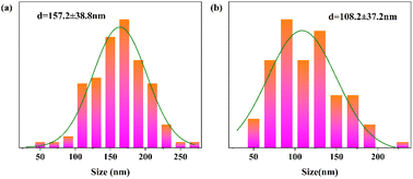
Fig. 1 shows SEM images of the WO3 films obtained using various structure-directing agents; it is clear that the structure-directing agent has an obvious effect on the morphology and structure of the products. The typical SEM image shows that the morphology of the samples was mainly 2D nanoplate (Fig. 1a) and nanosheet (Fig. 1b) arrays using oxalate and citric as the structure-directing agents, respectively. 3D nanospheres (Fig. 1c and d) and nanocages (Fig. 1e and f) were obtained using acetone and acetonitrile as the structure-directing agents, respectively. From Fig. 2a and b, it is clear that the average width of WO3 nanoplate and nanosheet were 157.2 and 108.2 nm, respectively. The diffusion length of photo-excited electrons and holes becomes shorter when the diameter decreases, which is beneficial for reducing the recombination of photo-excited electrons and improving photocatalytic performance. It can be seen from Fig. 1c that the obtained WO3 product represents flower-like hierarchical structures with a diameter of 7–8 μm. Fig. 1d shows the high-magnification SEM images of individual micro-flowers, showing that these WO3 assemblies consist of a large number of nanorods. Fig. 1e and f show the top view of WO3 films with approximate nanocage morphology. Apparently, the above experimental results indicate that acetone plays an important role in controlling the morphology of the WO3 microstructure. This distinctive nanostructure produced a rough surface, which provided a larger surface area for the reactions occurring in the photocatalytic processes.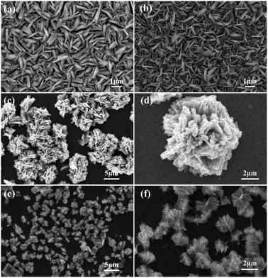 | ||
| Fig. 1 SEM images of the (a) WO3 nanoplate, (b) WO3 nanosheet, (c and d) WO3 nanosphere, and (e and f) WO3 nanocage. | ||
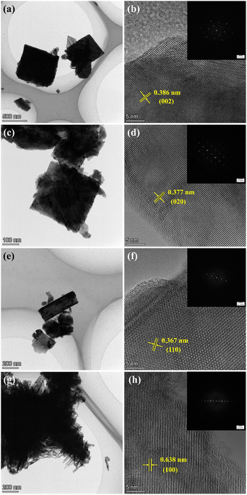
Fig. 3 shows the TEM and HRTEM images of WO3 films. Fig. 3a and c reveal typical TEM images of 2D monoclinic WO3 nanoplate/nanosheet arrays, further confirming their typical sheet-like structure morphology. The characteristic spacings of 0.386 nm (Fig. 3b) and 0.377 nm (Fig. 3d) in the HRTEM images correspond to the (002) and (020) lattice planes of monoclinic WO3, respectively. The TEM image of the WO3 nanosphere (Fig. 3e) shows the individual nanorod structure; the HRTEM image (Fig. 3f) indicates that the lattice fringes of 0.367 nm correspond to the (110) crystal plane of hexagonal WO3. The TEM image of the WO3 nanocage (Fig. 3g) reveals the dense branching structure and the lattice width of 0.638 nm in the HRTEM image (Fig. 3h) is attributable to the (100) plane of hexagonal WO3. The corresponding Fourier transition (FFT) patterns (inset in Fig. 3b, d, f, and h) suggest the single-crystalline nature of WO3 films.
Fig. 4 shows the XRD patterns of the as-prepared WO3 films. The XRD patterns of the 2D WO3 nanoplate and WO3 nanosheet exhibit a typical crystal structure of monoclinic WO3. The diffraction peaks at 23.1°, 23.6°, 24.4°, 26.6°, 28.9°, 34.2°, 41.9°, 49.9°, and 55.9° can be assigned to (002), (020), (200), (120), (112), (202), (222), (400), and (420) planes of monoclinic WO3 (JCPDS No. 83-0950), respectively. Compared to the 2D monoclinic WO3, the 3D nanosphere WO3 and WO3 nanocage show similar characteristic diffraction peaks of the hexagonal phase. The peaks at 14.0°, 22.8°, 24.4°, 26.8°, 28.2°, 33.6°, 36.6°,49.9°, and 55.6° corresponding to (100), (001), (110), (101), (200), (111), (201), (220), and (221) lattice planes of hexagonal WO3 (JCPDS No. 75-2187), respectively. All the diffraction peaks in the XRD patterns were sharp and distinct, confirming the high crystallinity of the samples. It is worth noting that WO3 with a hexagonal structure has one-dimensional large tunnels compared with other WO3 phases, which facilitate the transport of the conductive ions.17
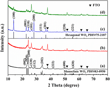 | ||
| Fig. 4 XRD patterns of the (a) WO3 nanoplate, (b) WO3 nanosheet, (c) WO3 nanosphere, and (d) WO3 nanocage. | ||
The schematic of the preparation process of the WO3 films is shown in Fig. 5. Normally, the inherent crystal structure and external reactions affect the crystal growth.18,19 First, the precursor of tungstic acid was synthesized by acidification with sodium tungstate, then due to the coordination of oxalate (or citrate) to the tungstic acid, a kind of water–dissolvable complex is generated and the complex is slowly hydrolysed and then polycondensed to WO3·H2O nanoplate (or nanosheet) crystal nuclei under hydrothermal conditions. The WO3·H2O nanoplates (or nanosheets) were completely converted into monoclinic WO3 after annealing. In this preparation method, WO3 nanoplates (or nanosheets) were directly grown on the FTO glass without a seed layer, this may have eliminated grain boundaries from the seed layers and could reduce the resistance between the FTO glass and the photocatalyst.
The properties of the solvent could play an important role in the growth of various forms of WO3 under solvothermal conditions. As the acetonitrile is dissolved in the solvent, the shape of the particle changes, resulting in hierarchical structures instead of nanosheets. This may be related to the solubility of the precursor in the solvent. The high solubility of acidified sodium tungstate in the mixed solvent of water and acetone would induce more uniform nucleation.20,21 Furthermore, acetone can interact with the oxygen ions close to the tungsten ion, mainly because the α-hydrogen of acetone is active, analogous to the interaction between acetone and germanium, silicon, or titania.22–24 The existence of tungstate anion impacts the synthesis of different crystalline tungsten trioxide, so the solubility of sodium tungstate is directly related to the solubility of tungstate, which affects its existence in the solution. The hexagonal phase WO3 was obtained when acetone or acetonitrile was added to the solvent.
3.2 Photocatalytic and photoelectrochemical performances
The photocatalysis properties of the WO3 films were investigated through the degradation of methylene blue (MB) and rhodamine B (RhB) reactions. As shown in Fig. 6, the crystal structure and morphology had an appreciable influence on the performance of WO3. The degradation rates of MB were 52.2%, 61.7%, 83.2%, and 72.4% after 120 min with m-WO3 nanoplates, m-WO3 nanosheets, h-WO3 nanospheres, and h-WO3 nanocages, respectively (Fig. 6a). As depicted in Fig. 6b, the MB degradation is compatible with the first-order reaction kinetics. The reaction rate of m-WO3 nanoplates, m-WO3 nanosheets, h-WO3 nanospheres, and h-WO3 nanocages were 5.83 × 10⁻³ min−1, 7.63 × 10⁻³ min−1, 13.67 × 10⁻³ min−1 and 10.03 × 10⁻³ min−1, respectively. In addition, the degradation rates of RhB were 56.8%, 70.2%, 87.9%, and 80.3%, respectively, and the corresponding reaction rates were 6.38 × 10⁻³ min−1, 9.87 × 10⁻³ min−1, 16.45 × 10⁻³ min−1, and 12.58 × 10⁻³ min−1, respectively (ESI Table S1†).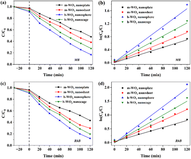 | ||
| Fig. 6 (a) Degradation of MB and (b) the corresponding kinetic curves. (c) Degradation of RhB and (d) the corresponding kinetic curves by the WO3 films. | ||
The 3D hierarchical h-WO3 nanosphere exhibited the highest photocatalysis activity, which is mainly due to the large specific surface area and small branched nanorod structure that enhanced photo-efficiency. The higher light absorption intensity and lower interface resistance facilitate more photogenerated holes to participate in the photocatalytic degradation process.
Fig. 7a shows the linear sweep voltammograms (LSV) of the as-prepared WO3 films photoanodes in the 0.5 M Na2SO4 electrolyte. As can be seen from Fig. 7a, the photocurrent density of the m-WO3 nanoplate photoanode is 0.05 mA cm−2 at 1.23 V vs. RHE, while the m-WO3 nanosheet photoanode showed a much higher photocurrent density of 0.13 mA cm−2, this indicates that the crystal structure had a certain influence on monoclinic WO3 samples. Extraordinary, the hierarchical structure of h-WO3 nanospheres showed the highest photocurrent density of 0.37 mA cm−2, which is 7.4 times higher than that of the m-WO3 nanoplate photoanode. The 3D hierarchical structure increases the optical absorption and effective separation of the photo-induced carriers and improves the photoelectric performance. Fig. 7b shows the transient photocurrent density responses at 1.2 V (vs. RHE) under chopped light illumination. It can be seen that all the WO3 films displayed immediate and good photo response behaviour.
Fig. 7c shows the electrochemical impedance spectroscopy (EIS) Nyquist curves of WO3 samples under open-circuit voltage and simulated sunlight illumination. For semiconductor photoelectrochemical reactions, the separation efficiency of the photo-generated carriers is the key factor, and the impedance of the semiconductor is determined by the diffusion mass transfer process and charge transfer resistance. The semicircle in the high-frequency region represents the charge-transfer resistance at the WO3/electrolyte interface, the smaller the diameter of the semicircle in the EIS spectrum, the lower would be the charge-transfer resistance.25
The semicircle radius in the Nyquist curve reflects the reaction rate on the electrode surface, the h-WO3 nanosphere hierarchical structures show a smaller semicircle radius, which means a lower charge transfer resistance and higher separation efficiency of the photogenerated electron–hole pairs.26 The 3D hierarchical structures with a large surface area, increase the contact area between photoanode and electrolyte, indicating a faster interfacial charge transfer, which is consistent with the photocurrent response results mentioned above.
3.3 Photocatalytic mechanisms
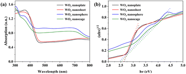
To investigate the mechanisms for the improvement of photocatalytic performance, the light absorption performance, the recombination of photogenerated charge carriers, and band structure were studied. Fig. 8 illustrates the UV-vis absorption spectra and the corresponding Tauc plots of the WO3 films. For the 2D monoclinic WO3 arrays, the absorption edge appears near the wavelength of 460 nm, it is consistent with the inherent band-gap absorption edge of WO3.The addition of acetone or acetonitrile has a significant effect on the optical properties of the films. Although the maximum absorption edge of the 3D hexagonal WO3 films is slightly blue-shifted, the light absorption intensity in the visible region is greatly increased with the addition of acetone or acetonitrile (425–700 nm).27,28 This phenomenon might be due to the absorption caused by multiple scattering in the multilevel branching structure of WO3. The optical band gap (Eg), was determined using the equation:
| αhv = A(hv − Eg) |
To investigate the influence of differences in WO3 crystal structure on the separation and transfer of photogenerated electrons and holes, the density of state (DOS) simulation calculations were conducted. As shown in Fig. 9a, monoclinic WO3 exhibited a perovskite-like structure by sharing the angles of the WO6 octahedron.31,32 While the WO6 octahedron is connected to a shared angle to form a six-membered ring in the ab plane of the hexagonal WO3, and stacked by sharing axial oxygen in the c-axis (Fig. 9c).
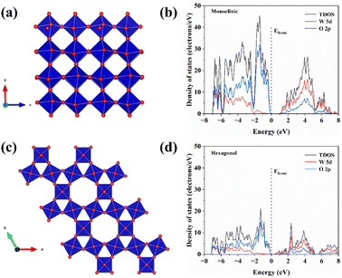 | ||
| Fig. 9 (a) Crystal structure model and (b) calculated DOS patterns of the monoclinic WO3 phase. (c) Crystal structure model and (d) calculated DOS patterns of the hexagonal WO3 phase. | ||
The partial density of states (PDOS) is the component of DOS in different orbitals, which shows the s, p, and d orbitals of each atom contribution to the total DOS. As the calculated DOS and PDOS depicted in Fig. 9b and d, the monoclinic and hexagonal WO3 have similar DOS spectra and electronic structures. The valence band maximum (VBM) potential of monoclinic and hexagonal WO3 is mainly contributed by O-2p orbital, while the conduction band minimum (CBM) potential for both samples is mainly from W-5d and a small portion of O-2p orbitals.
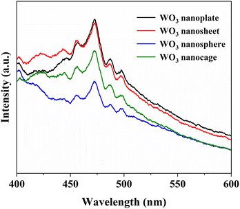
Fig. 10 shows the photoluminescence spectra of WO3 samples excited by 325 nm light at room temperature. In general, higher photoluminescence intensity shows a higher recombination rate of photoexcited electrons and holes, while lower PL intensity shows a lower recombination rate.33 The results showed that all films displayed a peak of similar photoluminescence spectra and the 3D h-WO3 nanosphere film exhibited the lowest fluorescence intensity, indicating the greater charge separation efficiency of the photogenerated electron and hole pairs. Moreover, the PL intensities of WO3 with hierarchical structures are obviously lower than that of 2D m-WO3 arrays. As shown in the previous optical absorption analyses, the hierarchical structure of the microspheres scatters the incident light, so the transmission path of the light in the WO3 is prolonged, the incident light is absorbed and used multiple times, so it can capture photons more effectively.
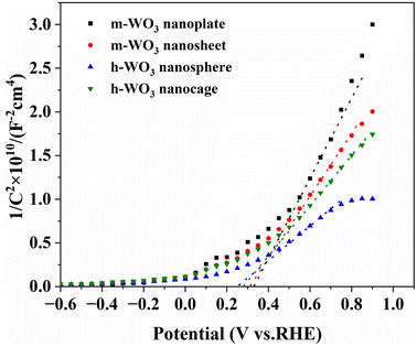
Mott–Schottky plots were recorded to investigate the flat band potentials (Vfb) and carrier density (Nd) of WO3 samples. The Mott–Schottky curves of WO3 films at 1000 Hz are shown in Fig. 11. The positive slopes present n-type semiconductor characteristics of all the WO3 films, indicating that electrons were the majority carriers in the as-prepared films. As shown in Fig. 11, the flat band potential of m-WO3 nanoplates, m-WO3 nanosheets, h-WO3 nanospheres, and h-WO3 nanocages were 0.33, 0.31, 0.26, and 0.28 V (vs. RHE), respectively. The smaller flat band potential of 3D h-WO3 nanosphere film implies a low overpotential, thus enhancing the photogenerated carrier's separation. However, the flat-band potential is 0.1–0.3 eV positive than the conduction band (CB) potential for the n-type semiconductors.34 Therefore, the ECB of m-WO3 nanoplates, m-WO3 nanosheets, h-WO3 nanospheres, and h-WO3 nanocages could be confirmed to be 0.13, 0.11, 0.06, and 0.08 eV, respectively. Combined with the above band gap, the valence band (VB) positions of m-WO3 nanoplates, m-WO3 nanosheets, h-WO3 nanospheres, and h-WO3 nanocages were 2.77, 2.72, 2.54, and 2.59 eV, respectively. The obtained energy band structure diagram is shown in Fig. S1 ESI.†
The carrier density (Nd) can be calculated using the following equation:35
4. Conclusions
In this study, WO3 films with different crystalline phases and morphologies were synthesized on FTO substrates using a template solvothermal process. Four types of WO3 films, including 2D monoclinic WO3 nanoplates, 2D monoclinic WO3 nanosheets, 3D hexagonal WO3 nanospheres, and 3D hexagonal WO3 nanocages can be prepared by adjusting the structure-directing agents. The hierarchical structure of the 3D WO3 films increased the surface area, enhanced light absorption, and promoted charge transfer, which resulted in higher performance than 2D WO3 films. In addition, the 3D WO3 nanosphere exhibited excellent photocatalytic activity and photocurrent density compared with other samples, which could be attributed to the large tunnels in the hexagonal-structured WO3, the lower charge transfer resistance, and the enhanced charge transfer efficiency. These findings contribute in several ways to our understanding of hierarchical structured materials and lay a good foundation for modifying their morphology.Conflicts of interest
There are no conflicts to declare.Acknowledgements
This work has been financially supported by the Provincial and Ministerial Co-construction of the Collaborative Innovation Center for Non-ferrous Metal New Materials and Advanced Processing Technology.Notes and references
- J. Zhang, X. Fu, H. Hao and W. Gan, J. Alloys Compd., 2018, 757, 134–141 CrossRef CAS.
- M. M. Khan, S. Kumar, T. Ahamad and A. N. Alhazaa, J. Alloys Compd., 2018, 743, 485–493 CrossRef CAS.
- G. Zheng, J. Wang, H. Liu, V. Murugadoss, G. Zu, H. Che, C. Lai, H. Li, T. Ding and Q. Gao, Nanoscale, 2019, 11, 18968–18994 RSC.
- C. J. Gao, X. W. Guo, L. W. Nie, X. Wu, L. M. Peng and J. Chen, Int. J. Hydrogen Energy, 2023, 48, 2442–2465 CrossRef CAS.
- M. S. Sharifiyan, A. Fattah-alhosseini and M. Karbasi, Ceram. Int., 2023, 49, 35175–35185 CrossRef CAS.
- J. Zhou, S. Lin, Y. Chen and A. Gaskov, Appl. Surf. Sci., 2017, 403, 274–281 CrossRef CAS.
- M. Farhadian, P. Sangpour and G. Hosseinzadeh, J. Energy Chem., 2015, 24, 171–177 CrossRef.
- W. Li, J. Li, X. Wang, J. Ma and Q. Chen, Int. J. Hydrogen Energy, 2010, 35, 13137–13145 CrossRef CAS.
- I. M. Szilágyi, B. Fórizs, O. Rosseler, Á. Szegedi, P. Németh, P. Király, G. Tárkányi, B. Vajna, K. Varga-Josepovits and K. László, J. Catal., 2012, 294, 119–127 CrossRef.
- M. Aslam, I. M. Ismail, S. Chandrasekaran and A. Hameed, J. Hazard. Mater., 2014, 276, 120–128 CrossRef CAS PubMed.
- R. Velmurugan, M. Aishwarya, K. Balamurugan, K. Nivedha and B. Subramanian, Electrochim. Acta, 2022, 419, 140371 CrossRef CAS.
- M. M. Mohamed, T. M. Salama, M. Hegazy, R. M. Abou Shahba and S. Mohamed, Int. J. Hydrogen Energy, 2019, 44, 4724–4736 CrossRef CAS.
- Y.-J. Zhang, K.-K. Nie, L. Yi, B.-J. Li, Y.-L. Yuan, Z.-Q. Liu and W. Huang, Adv. Sci., 2023, 10, 2302301 CrossRef CAS PubMed.
- B.-J. Li, K.-K. Nie, Y.-J. Zhang, L.-X. Yi, Y.-L. Yuan, S.-K. Chong, Z.-Q. Liu and W. Huang, Adv. Mater., 2023, 35, 2303285 CrossRef CAS PubMed.
- S. Niu, S. Li, Y. Du, X. Han and P. Xu, ACS Energy Lett., 2020, 5, 1083–1087 CrossRef CAS.
- M. Saeed, I. Khan, M. Adeel, N. Akram and M. Muneer, New J. Chem., 2022, 46, 2224–2231 RSC.
- D. Ma, G. Shi, H. Wang, Q. Zhang and Y. Li, J. Mater. Chem. A, 2013, 1, 684–691 RSC.
- L. Xu, Y.-L. Hu, C. Pelligra, C.-H. Chen, L. Jin, H. Huang, S. Sithambaram, M. Aindow, R. Joesten and S. L. Suib, Chem. Mater., 2009, 21, 2875–2885 CrossRef CAS.
- Q. Ding, Y. Wang, P. Guo, J. Li, C. Chen, T. Wang, K. Sun and D. He, Sensors, 2020, 20, 3473 CrossRef CAS PubMed.
- Y. Zheng, G. Chen, Y. Yu, J. Sun, Y. Zhou and J. Pei, CrystEngComm, 2014, 16, 6107–6113 RSC.
- D. M. Griffiths and C. H. Rochester, J. Chem. Soc. Faraday Trans., 1978, 74, 403–417 RSC.
- L. Zhou, J. Zou, M. Yu, P. Lu, J. Wei, Y. Qian, Y. Wang and C. Yu, Cryst. Growth Des., 2008, 8, 3993–3998 CrossRef CAS.
- G. T. Wang, C. Mui, C. B. Musgrave and S. F. Bent, J. Am. Chem. Soc., 2002, 124, 8990–9004 CrossRef CAS PubMed.
- G. T. Wang, C. Mui, C. B. Musgrave and S. F. Bent, J. Phys. Chem. B, 2001, 105, 12559–12565 CrossRef CAS.
- Y. Liu, F. Y. Su, Y. X. Yu and W. D. Zhang, Int. J. Hydrogen Energy, 2016, 41, 7270–7279 CrossRef CAS.
- G. Zhang, C. Chen, M. Lu, C. Chai and Y. Wu, Mater. Chem. Phys., 2007, 105, 331–340 CrossRef CAS.
- Y.-G. Yu, G. Chen, L. X. Hao, Y. S. Zhou, Y. Wang, J. Pei, J. X. Sun and Z. H. Han, Chem. Commun., 2013, 49, 10142–10144 RSC.
- M. Zirak, O. Moradlou, M. Bayati, Y. Nien and A. Moshfegh, Appl. Surf. Sci., 2013, 273, 391–398 CrossRef CAS.
- Z.-H. Zheng, H. B. Lan, Z. H. Su, H. X. Peng, J. T. Luo, G. X. Liang and P. Fan, Sci. Rep., 2019, 9, 17422 CrossRef PubMed.
- T. Zhang, Y. Hou, V. Dzhagan, Z. Liao, G. Chai, M. Löffler, D. Olianas, A. Milani, S. Xu and M. Tommasini, Nat. Commun., 2018, 9, 1140 CrossRef PubMed.
- Z. Wang, C. Zhu, Z. Ni, H. Hojo and H. Einaga, ACS Catal., 2022, 12, 14976–14989 CrossRef CAS.
- J. Yang, X. Chen, X. Liu, Y. Cao, J. Huang, Y. Li and F. Liu, ACS Sustainable Chem. Eng., 2021, 9, 5642–5650 CrossRef CAS.
- H. Zhang, W. Tian, Y. Li, H. Sun, M. O. Tadé and S. Wang, J. Mater. Chem. A, 2018, 6, 6265–6272 RSC.
- C. Xu, Z. Jin, J. Yang, F. Guo, P. Wang, H. Meng, G. Bao, Z. Li, C. Chen and F. Liu, J. Environ. Chem. Eng., 2021, 9, 106337 CrossRef CAS.
- J. Bai, R.-T. Gao, X. Guo, J. He, X. Liu, X. Zhang and L. Wang, Chem. Eng. J., 2022, 448, 137602 CrossRef CAS.
Footnote |
| † Electronic supplementary information (ESI) available: See DOI: https://doi.org/10.1039/d3ra07329g |
| This journal is © The Royal Society of Chemistry 2024 |

