 Open Access Article
Charge transport mechanisms of PbSnSe2 and observation of transition from direct to Fowler–Nordheim tunneling
Qaisar
Abbas
a,
Syed Mesam Tamar
Kazmi
a,
Chuanbo
Li
b,
Xiulai
Xu
 cd and
M. A.
Rafiq
 *a
*a
aCondensed Matter Physics Laboratories, Department of Physics and Applied Mathematics, Pakistan Institute of Engineering and Applied Sciences, PO Nilore, Islamabad 45650, Pakistan. E-mail: aftab@cantab.net
bSchool of Science, Minzu University of China, Beijing 100081, China
cInstitute of Physics, Chinese Academy of Sciences, Beijing 100190, China
dState Key Laboratory for Mesoscopic Physics and Frontiers Science Center for Nano-optoelectronics, School of Physics, Peking University, Beijing 100871, China
First published on 14th February 2024
Abstract
In this study, we report the observation of various conduction mechanisms in mechanically exfoliated PbSnSe2 based on temperature-dependent current and voltage characteristics. A transition from direct tunneling to Fowler–Nordheim tunneling in PbSnSe2 was observed at 2.63 V. At lower temperatures, the 3D Mott variable range hopping model fits the data, yielding a density of states of ∼8.80 × 10²⁰ eV−1 cm−3 at 2 V. The values of Whop and Rhop were 64 meV and 22.7 nm, respectively, at 250 K. The Poole–Frenkel conduction was observed in the Au/PbSnSe2/Au device and the dielectric constant of PbSnSe2 was calculated to be 1.4. At intermediate voltages, a space charge limited current with an exponential distribution of traps was observed and a trap density of ∼9.53 × 1013 cm−3 and a trap characteristic temperature of 430 K were calculated for the Au/PbSnSe2/Au device.
Introduction
Ever since the successful isolation of monolayer graphene, which has intrinsic bandgap limitations, the quest for novel van der Waals materials exhibiting remarkable electronic properties has become an unceasing pursuit.1 In this relentless exploration, the metal chalcogenide family is the most well studied after graphenes, but large strides are made on other materials as well.2 Among these materials, group-IV monochalcogenides (MX: M = Pb and Sn and X = S, Se, and Te) have shown great potential in the fields of nanoelectronics,3 optoelectronics,4 sensors,5 catalysis,6 energy storage,7 and thermoelectric devices8 owing to their high carrier mobilities, high on/off ratios, tunable band structures, and excellent thermoelectric properties. Moreover, their low cost and earth abundance are considered ancillary advantages to other traits.9 PbSnSe2 is a ternary compound of group IV metal chalcogenides poised to unravel new paradigms in the field of nanoelectronics. Only a few computational studies have been reported on this material;10–12 however, experimental studies on PbSnSe2 have been overlooked.Therefore, we report the observations of various conduction mechanisms in mechanically exfoliated PbSnSe2 from the temperature-dependent current and voltage (IV) characteristics. A transition from direct tunneling (DT) to Fowler–Nordheim tunneling (FN) in PbSnSe2 was observed at 2.63 V. At lower temperatures, the Mott variable range hopping (VRH) model fits the experimental data well, yielding the Mott characteristic temperature, density of states, hopping distance, and average hopping energy of the charge carriers in PbSnSe2. Moreover, the dielectric constant of PbSnSe2 was approximated from the Poole–Frenkel emission at higher voltages. Subsequently, using the space charge limited current (SCLC) model, we evaluated the trap density using the crossover voltage and calculated the characteristic temperature and energy of these traps.
Experimental details
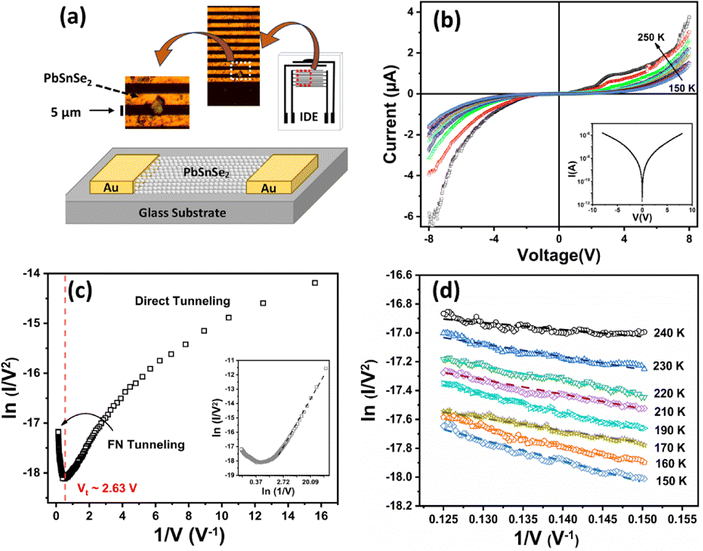
Pure PbSnSe2 crystals (purchased from Six Carbon Technology) were exfoliated using thermal release tape and transferred onto a silicon substrate with a thin layer of SiO2. The chosen flake of PbSnSe2 with a lateral size of ∼5 μm was then transferred to interdigitated electrodes (IDEs), as shown schematically in Fig. 1a, along with the optical image. IDE consisted of 10 comb-like pairs of gold electrodes 5 μm apart on a glass substrate. The temperature-dependent IV characteristics were recorded using an Agilent semiconductor parameter analyzer 4156C in a cryogenic probe station.Results and discussion
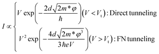
Fig. 1b shows the temperature-dependent nonlinear IV characteristics of PbSnSe2 from 150 K to 250 K. The inset of Fig. 1b shows that the switching in PbSnSe2 flakes is ∼105. This switching in Au/PbSnSe2/Au devices may find applications in PbSnSe2-based high-voltage resistive switching devices.13 As can be seen from Fig. 1b, the flake exhibits semiconducting behaviors. Xu et al.10 have shown that PbSnSe2 exhibits semiconducting behaviors if the number of layers in the flake is less than 8. Therefore, we suggest that the number of layers in the flake should be less than 8.Fig. 1c shows the ln(1/V2) vs. 1/V plot of the PbSnSe2 device at 220 K. This plot shows the change in behavior at a particular voltage at all temperatures. This change is observed at 1/V ≈ 0.38 V−1 (2.63 V), which segregates the plot into two distinct regions. These two regions correspond to FN tunneling and DT. When the externally applied voltage is smaller in magnitude than the barrier height, DT occurs, which corresponds to the tunneling of charge carriers through a trapezoidal barrier. In contrast, for voltages exceeding the barrier height, electrons tunnel through a triangular barrier, i.e., FN tunneling occurs, which is analogous to field emission. The tunneling current can be expressed using the following relation:14
 | (1) |
Using eqn (1), the fitted curves showed excellent agreement with the experimental data. The term ln(I/V2) exhibits a linear decrease at high voltages, which refers to FN tunneling. The logarithmic growth at low voltages implies that direct tunneling is the dominant transport mechanism in this region. The average value of the transition voltage was calculated to be approximately 2.63 V. Therefore, the barrier height is 2.63 eV according to the formula Vt = φ/e for the Au/PbSnSe2/Au device.15
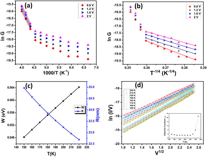
Fig. 2a shows the Arrhenius plot for studying the two different transport mechanisms: at high temperatures, thermally activated transport mechanism, whereas at low temperatures, data fit Mott's three-dimensional VRH model, as shown in Fig. 2b. This model obeys the following equation:16
 | (2) |
The pre-exponential factor G0 weakly depends on the temperature, and T0 is the Mott temperature related to the density of localized states whose relation is given by the following equation:17
 | (3) |
| Voltage (V) | T 0 (K) | N(EF) (eV−1 cm−3) |
|---|---|---|
| 0.8 | 7.38 × 10⁶ | 2.76 × 10²⁰ |
| 1.2 | 3.65 × 10⁶ | 5.58 × 10²⁰ |
| 1.6 | 2.96 × 10⁶ | 6.87 × 10²⁰ |
| 2.0 | 2.31 × 10⁶ | 8.80 × 10²⁰ |
Mott's VRH parameters also include the hopping distance (Rhop) and the hopping energy (Whop), which were calculated using the following equations:17
 | (4) |
 | (5) |
The graph is plotted for Rhop and Whop as a function of temperature, as shown in Fig. 2c. The decrease in the values of hopping distance is due to the increase in the disorder of the system with temperature.19 This leads to the conduction by hopping of carriers from states located closely in space to the initial state. In contrast, the hopping energy tends to increase with the increase in temperature. This is due to the fact that the increase in disorder requires extra energy for the carriers to make a transition from the initial to the final state.19
Fig. 2d shows that data at higher voltages obey the ln(σ) vs. V dependence, which is Poole–Frenkel emission. It refers to the thermal excitation of charge carriers trapped inside a potential well that are enhanced by an electric field. Conduction through the PF mechanism is given as follows:20
 | (6) |
 | (7) |
The inset of Fig. 2d shows that the value of the dielectric constant for PbSnSe2 in the temperature range of 150 K–220 K is approximately 1.4, which is much close to the values of the dielectric constant found for the ternary compound.10
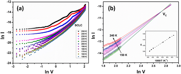
Fig. 3a shows the IV characteristics on a double logarithmic scale at intermediate voltages (150 K–250 K). The estimated values of the slopes vary in the range of ∼3–5. The values of slope increase while moving towards lower temperatures because the trapped electrons become more stable.22 A slope greater than two infers the presence of SCLC with an exponential distribution of traps and is given as follows:23
 | (8) |
Fig. 3b shows the ln![[thin space (1/6-em)]](https://www.rsc.org/images/entities/char_2009.gif) I–ln
I–ln![[thin space (1/6-em)]](https://www.rsc.org/images/entities/char_2009.gif) V graph, which meets at a specific point after extrapolating the lines and this single point is referred to as “cross-over voltage (Vc)”. The relation of Vc with the trap density is given by the following equation:19
V graph, which meets at a specific point after extrapolating the lines and this single point is referred to as “cross-over voltage (Vc)”. The relation of Vc with the trap density is given by the following equation:19
 | (9) |
From Fig. 3b, the cross-over voltage for PbSnSe2 flakes comes out to be 15.39 V. Using the value of εr = 1.4 and Vc in eqn (6), the trap density comes out to be 9.53 × 1013 cm−3. The inset of Fig. 3b illustrates that m increases linearly as a function of the inverse temperature, which is in agreement with the SCLC model. The characteristic temperature Tt comes out to be ∼430 K, which leads to a characteristic energy of 37 meV.
Conclusions
In summary, a transition from direct tunneling to FN tunneling in an Au/PbSnSe2/Au device was observed at 2.63 V. The values of N(EF) estimated using the 3D Mott VRH model (p = 1/4) were found to be 2.76 × 10²⁰ to 8.80 × 10²⁰ eV−1 cm−3 at 0.8 to 2 V, respectively. Moreover, the values of Whop and Rhop were calculated to be 48 meV and 25 nm, respectively, at 150 K. Whereas at 220 K, the values of Whop and Rhop were 64 meV and 22.7 nm, respectively. The data fitting proved that Poole–Frenkel emission is the dominant conduction mechanism, which led to the calculation of the dielectric constant (∼1.4). At intermediate voltages, SCLC with an exponential distribution of traps was observed in the Au/PbSnSe2/Au device, and from this model, the trap density turned out to be ∼9.53 × 1013 cm−3. Moreover, the characteristic trap temperature and energy of this device were calculated to be 430 K and 37 meV, respectively.Data availability
Data sharing is not applicable to this article as no new data were created or analysed in this study.Author contributions
Qaisar Abbas: investigation (equal); writing – original draft (equal); writing – review and editing (equal). Syed Mesam Tamar Kazmi: investigation (equal); writing – original draft (equal); writing – review & editing (equal). Chuanbo Li: investigation (supporting); resources (equal). Xiulai Xu: investigation (supporting); resources (equal). M. A. Rafiq: investigation (equal); writing – original draft (equal). writing – review & editing (equal); resources (equal); supervision (equal).Conflicts of interest
The authors have no conflicts of interest to disclose.References
- R. Frisenda, Y. Niu, P. Gant, M. Muñoz and A. Castellanos-Gomez, npj 2D Mater. Appl., 2020, 4, 38 CrossRef.
- S.-L. Li, K. Tsukagoshi, E. Orgiu and P. Samorì, Chem. Soc. Rev., 2016, 45, 118–151 RSC.
- W. Prost, F. Kruis, F. Otten, K. Nielsch, B. Rellinghaus, U. Auer, A. Peled, E. Wassermann, H. Fissan and F. Tegude, Microelectron. Eng., 1998, 41, 535–538 CrossRef.
- K. V. Chandekar, F. H. Alkallas, A. B. G. Trabelsi, M. Shkir, J. Hakami, A. Khan, H. E. Ali, N. S. Awwad and S. AlFaify, Phys. B, 2022, 641, 414099 CrossRef CAS.
- A. Munoz, J. Melendez, M. Torquemada, M. Rodrigo, J. Cebrian, A. De Castro, J. Meneses, M. Ugarte, F. López and G. Vergara, Thin Solid Films, 1998, 317, 425–428 CrossRef CAS.
- Z. Tachan, M. Shalom, I. Hod, S. Ruhle, S. Tirosh and A. Zaban, J. Phys. Chem. C, 2011, 115, 6162–6166 CrossRef CAS.
- S. Majumder, S. Karade, R. Kumar, M. Gu, B. R. Sankapal and K. H. Kim, J. Alloys Compd., 2022, 906, 164323 CrossRef CAS.
- W. Liang, O. Rabin, A. I. Hochbaum, M. Fardy, M. Zhang and P. Yang, Nano Res., 2009, 2, 394–399 CrossRef CAS.
- L. C. Nhan, V. T. T. Vi, D. X. Du, N. Q. Cuong, N. N. Hieu and T. P. T. Linh, Chem. Phys., 2023, 566, 111797 CrossRef CAS.
- W. Xu, Z. Xie, J. Su, R. Wang, X. Wu and H. Xu, J. Phys. Chem. Lett., 2021, 12, 10574–10580 CrossRef CAS PubMed.
- T. Wang, X. Duan, H. Zhang, J. Ma, H. Zhu, X. Qian, J. Y. Yang, T. H. Liu and R. Yang, InfoMat, 2023, e12481 CrossRef CAS.
- C.-H. Ding, Z.-F. Duan, N.-N. Luo, J. Zeng, W. Ren, L.-M. Tang and K.-Q. Chen, Nanomaterials, 2023, 13, 1519 CrossRef CAS PubMed.
- S. Pandey, C. Biswas, T. Ghosh, J. J. Bae, P. Rai, G.-H. Kim, K. J. Thomas, Y. H. Lee, P. Nikolaev and S. Arepalli, Nanoscale, 2014, 6, 3410–3417 RSC.
- J. M. Beebe, B. Kim, J. W. Gadzuk, C. Daniel Frisbie and J. G. Kushmerick, Phys. Rev. Lett., 2006, 97, 026801 CrossRef.
- T. Ikuno, H. Okamoto, Y. Sugiyama, H. Nakano, F. Yamada and I. Kamiya, Appl. Phys. Lett., 2011, 99, 023107 CrossRef.
- N. F. Mott, Philos. Mag., 1969, 19, 835–852 CrossRef CAS.
- L. Zhang and Z.-J. Tang, Phys. Rev. B: Condens. Matter Mater. Phys., 2004, 70, 174306 CrossRef.
- Q. Liang, Q. Zhang, X. Zhao, M. Liu and A. T. S. Wee, ACS Nano, 2021, 15, 2165–2181 CrossRef CAS PubMed.
- Z. Imran, M. A. Rafiq and M. M. Hasan, AIP Adv., 2014, 4, 067137 CrossRef.
- M. Choueib, A. Ayari, P. Vincent, S. Perisanu and S. Purcell, J. Appl. Phys., 2011, 109, 073709 CrossRef.
- J. R. Yeargan and H. L. Taylor, J. Appl. Phys., 2003, 39, 5600–5604 CrossRef.
- M. Rafiq, Y. Tsuchiya, H. Mizuta, S. Oda, S. Uno, Z. Durrani and W. Milne, Appl. Phys. Lett., 2005, 87, 182101 CrossRef.
- S. M. T. Kazmi, Z. Zahoor, N. T. Yusra, M. H. Bhatti, M. F. Afsar, F. Sher, H.-u. Rashid and M. A. Rafiq, Phys. B, 2023, 670, 415400 CrossRef CAS.
| This journal is © The Royal Society of Chemistry 2024 |


