DOI:
10.1039/D3RA08759J
(Paper)
RSC Adv., 2024,
14, 5234-5247
Lattice vibration modes and electron–phonon interactions in monolayer vs. bilayer of transition metal dichalcogenides
Received
22nd December 2023
, Accepted 19th January 2024
First published on 9th February 2024
Abstract
Transition metal dichalcogenides are at the center of intense scientific activity due to their promising applications, as well as the growing interest in basic research related to their electronic and dielectric properties. The layered structure of single-(ML) and two-layer (2ML) samples presents exciting features for light–matter interaction, electron transport, and electronic and optoelectronic applications. Lattice vibrations and electron–phonon interactions are essential for studying the above mentioned topics. Phonon spectra in ML and 2ML of MoX2 and WX2 (X = S, Se, and Te) families are studied using first principles calculations. A comprehensive analysis of the two-dimensional optical–phonon dispersion laws is performed, and the results illustrate the main differences between ML and 2ML for each considered semiconductor. Taking advantage of ab initio calculations, a generalization of the phenomenological Born–Huang dielectric model for long-wavelength vibrational modes around the Γ-point of the Brillouin zone (BZ) in 2ML structures is implemented. Explicit expressions are derived for the optical phonon dispersion of in-plane and out-of-plane normal modes. The set of characteristic parameters describing each long-wavelength optical branch is resolved from a direct comparison with the exact dispersion laws provided using the first principles calculations. The long-range electron–phonon Pekar–Fröhlich (PF) interaction and intra-valley electron scattering rates at the K-point of the BZ via E′ (LO) and Eul longitudinal optical oscillations are examined for the ML and 2ML structures, respectively. The non-local macroscopic screening and the coupling between the in-plane electric field and longitudinal optical mechanical oscillation, profoundly affect the PF Hamiltonian and the carrier inverse relaxation time.
I. Introduction
Transition metal dichalcogenides (TMDs) are an important class of materials in two dimensions (2D);1 they can be represented by the formula MX2, where M (Mo or W) is the transition metal element and X the chalcogenides (S, Se, or Te). In the X-M-X structure, the chalcogenide atomic layers are separated by a layer of metal atoms, forming a sandwich structure similar to two stacked hexagonal layers. The stacking can preferably form three polytypes: 2H hexagonal honeycomb, 1T trigonal, or 3R rhombohedral.2,3 Unlike graphene (zero band gap), the electronic structure of TMDs possess gaps around 1–2 eV;4 for instance, bulk MoS2 possesses an indirect band gap of 1.3 eV, while the monolayer (ML) possesses a direct gap of 1.8 eV.5–7 TMDs have shown promise as a potential replacement for silicon-based electronics due to their high carrier mobility,8 on/off ratio field-effect transistors,9 and compatibility with existing semiconductor manufacturing processes. Due to their unique optical properties,10 they are also being explored for use in various optoelectronic devices,11 such as solar cells,12 light-emitting diodes (LEDs),13 and photodetectors.14 They also have potential applications in sensing technologies, gas sensing15 and bio-sensing,16 due to their high surface-to-volume ratio and sensitivity to changes in the local environment. Furthermore, they might find applications in spintronics;17 this field involves the manipulation of electron spin for use in information processing due to their strong spin–orbit coupling and tunable band gap.
In general, the properties of several stacked layers differ from the ML behavior.18 For example, graphene changes from linear to parabolic dispersion,19 and even if we rotate the layers,20 unexpected phenomena such as superconductivity appear.21 Two layers of polar materials lead to the appearance of spontaneous ferroelectric properties22,23 in materials like hexagonal boron nitride24,25 or TMDs.26 By stacking two ferromagnetic layers, we can control the magnetic phase of the system with an external electric field.27,28 In addition to ferroelectricity applications, 2ML, and multilayer TMDs exhibit a higher density of states, carrier mobility, and stability at room temperature, giving them superior performance in various applications.29–34
For studies of electronic transport,35 optoelectronic applications,36,37 phonon damping,38 limited phonon mobility,39 quantum phononics,40 magneto-polaron resonances,41 dielectric and optical properties,42 in 2D structures, it is necessary to address the role of the phonon spectra and its interactions with charge carriers in these novel materials. The layered single and 2ML structures present interesting features for light–matter interactions and the aforementioned topics. Optical phonons in the ML of TMD are known to play a central role in several processes.43–45
Furthermore, the strength of the electron–phonon interaction must depend on the environment and the number of layers of the TMD compound. This raises several questions about what the phonon spectra, their symmetry, and the electron–phonon interaction are like for a ML or a 2ML TMD, in addition to being able to establish the differences between both considered structures.
The main objective of this work is to describe the effects on the phonon branches of the ML vs. 2ML in TMD semiconductors. To accomplish this task, in this article we have employed density functional perturbation theory (DFPT) to obtain the complete phonon spectra of MX2 compounds. The developed microscopic calculations support a phenomenological approach to simulate the small moment limit for optical phonon scattering laws in bilayers. We divided the study into polar and non-polar modes for the in-plane and out-of-plane atom oscillations for better analysis and comparative purposes. Having access to the analytical model within ab initio parameters describing the in-plane polar mode, we build the Pekar–Fröhlich (PF) Hamiltonian, allowing us to identify the key elements that govern the electron–phonon interaction.
The paper is organized as follows. First, we evaluate the phonon dispersion curves of single-layer and the bilayer of MX2 materials based on ab initio calculations. We provide a detailed discussion of the symmetry properties and the main differences of the optical branches present in the ML and bilayer of the MoX2 and WX2 families. Employing the results obtained from first principles calculations, in Section III we generalize a phenomenological model for long-wavelength optical modes for in-plane and out-of-plane TMD bilayer oscillations. Based on the ab initio results of the normal optical modes, we report the characteristic parameters that support the long-wavelength model for each phonon symmetry of MoX2 and WX2 materials. Finally, Section IV is devoted to the evaluation of the electrons’ intra-valley relaxation time due to the longitudinal phonon of ML and 2ML WX2 compounds. We use the first principles formalism to derive the electron–phonon PF interaction Hamiltonian and compare the single-layer’s scattering rates versus the bilayer. The conclusions are listed in Section V. Appendixes A–D report the parameters obtained by the DFPT calculations and summarize the main results for the polar modes in the framework of the phenomenological model.
II. Phonon dispersion
The phonon dispersion was computed using DFPT46 as implemented in the Quantum Espresso package.47 The exchange and correlation functional with dispersion interaction optB86b-vdW48,49 was used. The projector augmented wave method was used for the electron–core interaction with standard potential files from PSLibrary version 1.0.0.50 Periodic boundary conditions are implicit in Quantum Espresso. The supercell included a vacuum region to simulate the bidimensionality of ML and 2ML; also, a 2D cutoff was applied to the Coulomb interaction.51 The vacuum width was initially 10 Å, but it was enlarged to ensure that the out-of-plane components of the stress tensor are also less than 1 kbar. Tables 3 and 4 report the most important parameters. The atomic positions and in-plane lattice vectors were relaxed until all force components were smaller than 0.001 Ry/bohr, and all stress tensor components were smaller than 1 kbar. The out-of-plane dimension of the simulation cells (vector c), which control the vacuum widths, were kept fixed during the relaxation. The final lattice vectors are given in Table 3.
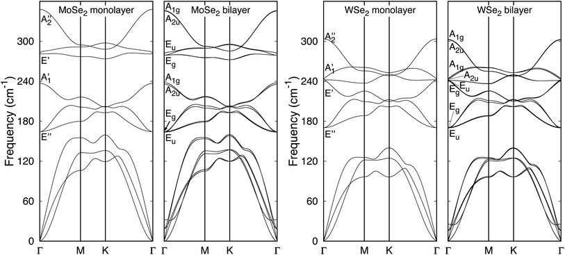
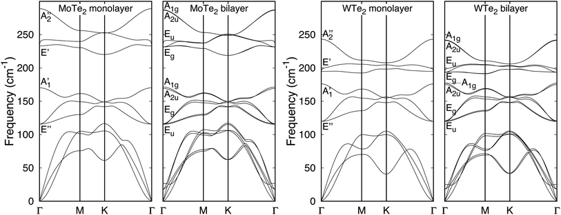
The complete phonon dispersion laws of ML and 2ML of MoX2 and WX2 (X = S, Se, Te) are shown in Fig. 1–3. First, notice that for each TMD, the 2ML spectrum is quite similar to the ML one. The main differences between both structures are: (1) small band splittings, (2) the appearance of low-frequency optical bands (less than 50 cm−1), (3) the branch of acoustic flexural mode – seen in quadratic dispersion around Γ – looks steeper in the bilayers, which is expected due to increased resistance to bending compared to ML. Other differences that can be appreciated in zoomed-in plots, concerning behavior at low wavevector, will be discussed below.
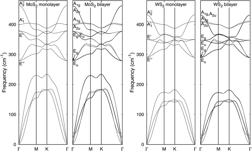 |
| | Fig. 1 Phonon dispersion curves of ML and 2ML of MoS2 and WS2 employing DFPT. Phonon momenta are along the high symmetry path Γ–M–K–Γ. | |
 |
| | Fig. 2 DFPT phonon spectra of ML and 2ML of MoSe2 and WSe2. | |
 |
| | Fig. 3 DFPT phonon spectra of ML and 2ML of MoTe2 and WTe2. | |
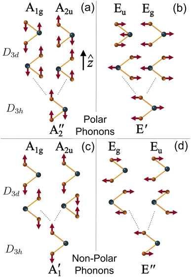
The symmetry groups of the Γ-point normal modes are D3h and D3d for the ML and 2ML, respectively.52 For a ML there are six optical modes that for a small wavevector are divided into three classes: longitudinal in-plane modes (LO1 and LO2), transverse in-plane modes (TO1 and TO2) and out-of-plane modes (ZO1 and ZO2).53 These modes correspond to the following irreducible representations of the group D3h: E′ (LO2 and TO2), E′′ (LO1 and TO1),  (ZO2) and
  (ZO1). The patterns of these modes are shown in Fig. 4, while labels indicate their location in the spectra of Fig. 1–3. For each branch of a ML, there are two normal modes of the 2ML. Hence, we have twelve long-wave optical branches: eight vibrating in-plane with symmetries Eg and Eu and four modes oscillating out-of-plane with symmetries A1g and A2u. Three low-frequency optical modes result from combining acoustical modes from the two layers. These modes are not discussed in this article. The vibration patterns displayed in Fig. 4 allow us to understand some trends in the family. In the normal modes E′′ (Eu, Eg) and
  (A2u, A1g) in the ML (2ML), the anions move, while the cation is at rest. The obtained frequencies of each mode differ in less than 4% between MoX2 and WX2. This can be understood if the interatomic force constants are nearly identical for Mo and W with the same anion. On the other hand, in the modes E′ (Eu, Eg) and
  (A2u, A1g), the cation motion opposes the motion of the anions. As discussed below, this motion is associated with the reduced mass μ given by 1/μ = 1/mM + 1/(2mX). Assuming again that the interatomic force constants do not depend on the cation, the frequency of these modes is proportional to
  . Renormalizing the frequencies of MoX2 modes by the factor
  provides an approximation to the frequencies of WX2. When the anion is changed, rescaling by the reduced mass leads to increased errors, suggesting that the force constants depend more strongly on the nature of the anion than the nature of the cation. Even then, the reduced mass helps to understand another trend. The frequencies in the sulfide monolayers increase in the order E′′, E′,
  ,
,  . However, the order E′,
  is reversed in MoSe2 and the tellurides. For
  frequencies, the atomic mass rescaling factor
  is 0.64 and 0.5 for X = Se and Te, respectively. For the E′ frequencies, the reduced mass scaling factor
  is 0.80 and 0.74 for X = Se and Te, respectively. Hence, the
  frequency decreases more than the E′ frequency due to the mass rescaling factor. Moreover, in the case of WSe2, both
  and E′ become almost degenerate (242 vs. 239 cm−1).
 |
| | Fig. 4 Atomic displacement patterns and symmetries of phonon branches for the ML and 2ML of the MX2 samples. Vibrations involving only the anion atoms (orange dots) are non-polar modes, while those cation oscillations opposing the anions’ motion (dark green dots) are polar. Each mode in a bilayer has two independent modes vibrating in and out of phase. The oscillations are divided into two independent groups: polar and non-polar phonons. | |
III. Long wavelength optical modes in TMD bilayers
In ref. 53, we developed a phenomenological continuum approach, based on ab initio calculations, that allowed us to describe the 2D optical vibrations of several TMD monolayers. We thoroughly analyzed the long wavelength phonon dispersion curves for in-plane and out-of-plane oscillations. In this section, we generalize this model to evaluate the optical vibration modes in TMD 2MLs.
A. Basic equations
The point group D3d presents an inversion center (see Fig. 4), so the phonon oscillation patterns can be classified in-phase and anti-phase. Next, the oscillation vectors Uip and Uap will describe the in-phase and anti-phase motion of the atoms for the two independent normal modes. The 2D TMD unit cell is unfolded into two single sub-cells I and II with a van der Waals interaction. Therefore, we can construct the normal oscillations for the bilayer by combining the in-phase or anti-phase motion of the individual sub-cells I and II. These two combinations have different symmetry representations with similar optical phonon dispersion, and due to the weak interlayer van der Waals coupling, they must show almost the same phonon energies.
B. Modes vibrating out-of-plane
Out-of-plane vibrations have A-symmetry. For the sake of clarity, we divide the study into two groups: (i) polar and (ii) non-polar modes (see normal vibration patterns in Fig. 4(a) and (c)).
1. A1g and A2u-non-polar phonons. Following the oscillation pattern shown in Fig. 4(c), the mass of the metal atoms Mi (i = 1, 2) are at rest, while only the chalcogen atoms (x1, x2) and (x3, x4) located at the first and second layer vibrate. The relative vector displacements UI = (ux1 − ux2)/2 and UII = (ux3 − ux4)/2 describe the opposing motion of the two chalcogen atoms Xi (i = 1, 2 or 3, 4) in the single-layer of reduced mass μ−1 = 2/mX. The anti-phase and in-phase displacements are given by Uap = (UI − UII/2 and Uip = (UI + UII)/2. The mechanical equation of motion reads as| | |
ρmω2U = γ·U ± β[∇∇·U − ∇ × ∇ × U],
| (1) |
where
ωA1g and ωA2u are the natural frequencies at phonon wave vector q = 0 with symmetry A1g and A2u, respectively, ρm is the 2D reduced mass density of a single-layer, β a tensor describing the quadratic parabolic behavior of phonon dispersion with q vector.Since the vector U(ρ) is parallel to the z-axis, eqn (1) decouples into two independent equations
| |
 | (2) |
The choice of the sign + or − depends on the curvature of the dispersion relation of the TMD material under consideration. From eqn (2) we get the dispersion relation:
| |
 | (3) |
2. A1g and A2u-polar phonons. The opposite motion of the chalcogen atoms (x1, x2) and (x3, x4) with respect to the transition metals (M1, M2) are responsible for the branches A1g and A2u (see Fig. 4(a)). The vector displacements, which describe the out-of-plane oscillation in the single layers I and II, are UI = uM1 − (ux1 + ux3)/2 and UII = uM2 − (ux3 + ux4)/2 with reduced mass μ−1 = mM−1 + (2mx)−1. The normal oscillations for the Uip in-phase and the Uap anti-phase correspond to A2u and A1g polar phonon modes, respectively. The relative displacement of atoms in the single-cell, I or II, or equivalently the atomic displacements UI and UII, generate a macroscopic electric field. For the in-phase oscillation Uip, we are in the presence of a non-zero internal electric field Ez. This field is coupled with the mechanical displacement Uip. Let us symbolize this linkage between the mechanical and the electric fields by the unknown constant αA2u. The mechanical equation of motion for Uip can be cast as| |
 | (4) |
where Ez(ρ,z) is the z-component of the electric field in the bilayer (we will assume that Ez(ρ,z) ≈ Ez(ρ,0)), ω0A2u the natural frequency at q = 0 with symmetry A2u, βA2u represents the quadratic behavior in q of the phonon dispersion. Due to the appearance of an internal electric field to the equation of motion (4) we must add the Maxwell’s equations that couples the mechanical motion Uip, Ez and the z-component of the macroscopic polarization (see Appendix B). It is possible to show that the dispersion relations for the polar phonon A2u vibrating out-of-plane are| |
 | (5) |
where ωA2u is the renormalized frequency at Γ. The out-of-phase amplitude Uap does not produce an electric field; therefore, the total internal electric field in the bilayer can be set to zero. Consequently, we can assume a similar eqn (4) but with Ez = 0. Thus, for the A1g mode:| |
 | (6) |
where ωA1g and βA1g are the natural frequency at Γ and the parabolicity parameter, respectively. Note that the A1g mode is Raman-allowed in the backscattering configuration with parallel configuration (X,X), and it is absent for cross-polarization (X,Y) under normal incidence.54 In the case of a single-layer, this mode is infrared Raman (IR) active. Due to the inversion center in the bilayer, the construction of the anti-phase solution Uap leads to the generation of Raman active mode A1g.55 This fact has been observed in WSe2, TaSe2, and MoTe2.56 The A2u phonon of the bilayer, as in the bulk, is still IR active.
C. Modes vibrating in-plane
In-plane phonons have E-symmetry. For the ML, the single-unit cell has two irreducible representations E′ and E′′. The modes with E′-symmetry are polar, while those with E′′ are non-polar (see in Fig. 4(b) and (d) the scheme of the vibration patterns and symmetries for the ML and bilayer). In general, modes vibrating in-plane have similar characteristics to those oscillating out-of-plane. Each single-layer mode has two branches of the 2ML: in-phase and anti-phase. These combinations belong to two different symmetry representations Eg and Eu. All E-modes are doubly degenerate at Γ.
1. Eu and Eg-non-polar phonons. Phonon modes with symmetry Eu and Eg are responsible for four optical branches. Two of them move in-phase and two in anti-phase of the atoms Xi (i = 1, 2, 3, 4) (we follow the same notation as in Subsection (III B 1)). Here, we are in the presence of two different sub-spaces that provide two independent equations of motion. A general equation of motion for the atom’s in-phase and out-of-phase motion can be written as| | |
ρmω2U = γ·U ± (βL·∇∇·U − βT·∇ × ∇ × U),
| (7) |
where γ, βL (βT) are given by
ωEg, ωEu are the natural frequencies in-plane at Γ,  and
and  are the phenomenological parameters obtained by the phonon dispersion ω(q). Using the solution Uip (Uap) = Uoi(Uoa)eiq·ρ we get
| |
 | (8) |
The same equation follows for the anti-phase component Uoa with ωEg → ωEu. Taking Uo = Ul + Ut, where q·Ut = 0, q·Ul ≠ 0, q × Ut ≠ 0, q × Ul = 0 we have two branches for phonons with Eg-symmetry, longitudinal and transverse with
| |
 | (9) |
For the Eu-symmetry we have the dispersion relation:
| |
 | (10) |
2. Eu and Eg-polar phonons. Each vibration mode in a single layer of MX2 is split into two modes in the bilayer: E′ → 2Eg and 2Eu. The movement of the in-plane phonon is determined by the oscillation of the positive ion relative to the negative ions: UI = uM1 − (ux1 + ux2)/2 and UII = uM2 − (ux3 + ux4)/2 for subcells I and II, that is, the M-atom vibrates opposed to the phase of the X-atoms in the layer.
Eg-phonon. Assuming that the out-of-phase amplitude Uap carries no net electric field, the Eg-optical vibrations are ruled by| |
 | (11) |
thus, we obtain the phonon dispersion for the longitudinal and transverse phonon:| |
 | (12) |
Eu-phonon. The opposite motions of the ions Mi (i = 1, 2) and Xi (i = 1, 2, 3, 4) lead to the appearance of a 2D electric field E(ρ,0) in the plane of the two layers. The equation of motion for the in-phase vector displacement Uip of the atoms involved is written as| |
 | (13) |
where α is the coupling constant between the mechanical oscillation Uip and the in-plane electric field E,53 ρm is the 2D reduced mass density with μ−1 = mM−1 + (2mX)−1, and ωEu the natural frequency at Γ. Eqn (13) provides the phonon dispersion relations (see Appendix C)| |
 | (14) |
and| |
 | (15) |
with r0 = 2πα2 being the screening parameter of the bilayer.
D. Phonon parameters
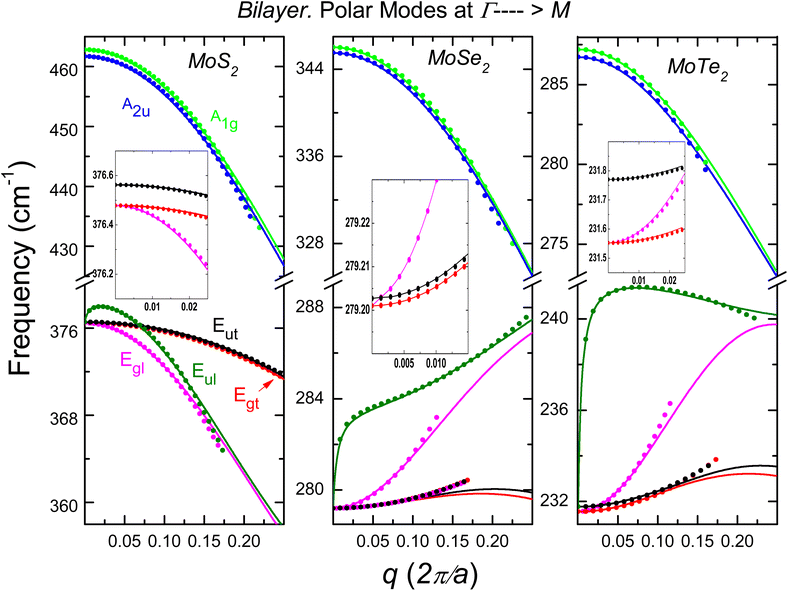
Fig. 5–8 compare ab initio calculations and the long-wave optical model for the MoX2 and WX2 families. For each family, the results are divided into polar and non-polar branches.
 |
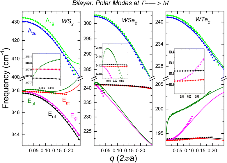
| | Fig. 5 Dispersion law of optical phonons for a bilayer of MoS2, MoSe2 and MoTe2. Out-of-plane phonons: A1g (green line) and A2u (blue line). In-plane modes with symmetries Eg and Eu split into Egl (magenta line), Egt (red line), Eul (olive line) and Eut (black line). The insets show the phonon dispersion for the Egl, Egt and Eut modes in the range q → 0. | |
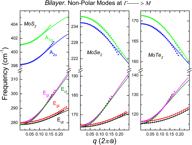 |
| | Fig. 6 The same as Fig. 5 but for the dispersion law of non-polar optical phonon dispersion. | |
 |
| | Fig. 7 Polar optical phonon dispersion for a bilayer of WS2, WSe2 and WTe2. Out-of-plane phonons: A1g (green line) and A2u (blue line). In-plane-modes with symmetries Eg and Eu split into Egl (magenta line), Egt (red line), Eul (olive line) and Eut (black line). The insets show the phonon dispersion of WS2 and WSe2 in the range q → 0, while for WTe2 only the Egl, Egt and Eut modes are shown. | |
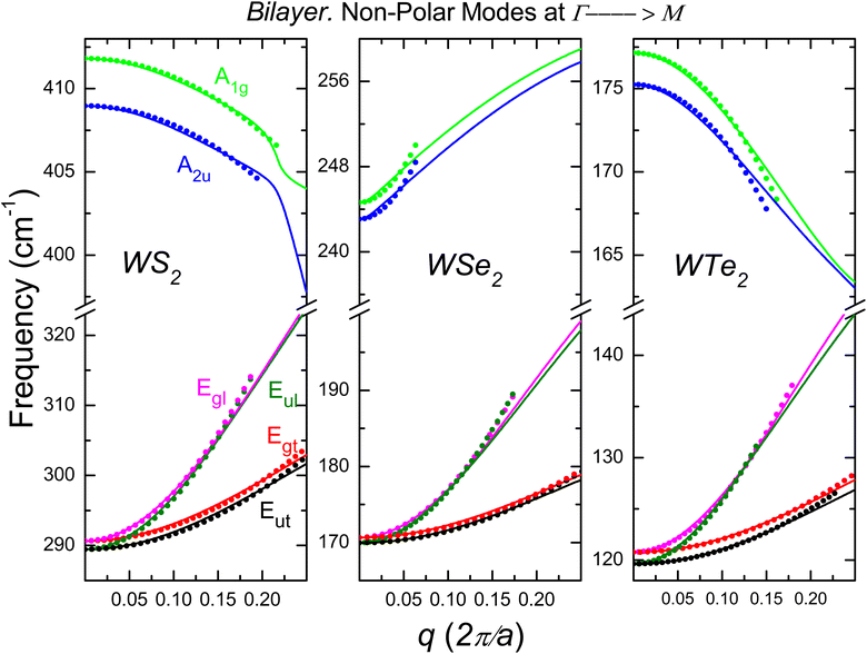 |
| | Fig. 8 The same as Fig. 7 but for the dispersion law of non-polar optical phonon dispersion. | |
1. MoX2 family. In Fig. 5 and 6 we show the optical phonon dispersion law, ω(q) of the 2ML MoX2 and phonon wave vectors q ≤ 0.25 (2π/a). The twelve phonon modes 2A2u, 2A1g, 2Eul, 2Eut, 2Egl and 2Egt are shown along the Γ → M-direction of the BZ. The dispersion relations obtained in Section II using the ab initio procedure are displayed by straight lines. The dots show the results using the long-wave polar optical model of Section III.
2. WX2 family. Fig. 7 and 8 are devoted to the 2A2u, 2A1g, 2Eul, 2Eut, 2Egl and 2Egt phonon dispersion branches for 2ML of WX2. We employed the same notation as Fig. 5 and 6.The Fig. 5–8 show that the precision achieved between the phenomenological treatment and first principles calculations depends on the optical branch and the material. The in-plane branches with E′ (polar modes) and E′′ (non-polar modes) symmetry are double-degenerates vibrating along the perpendicular longitudinal (Egl, Eul) and transverse (Egt, Eut) directions. Taking into account the phonon dispersion laws in Fig. 1–3, one can extract the parameters that govern the long-wave phenomenological model shown in Fig. 5–8. In Table 1, we report the relevant parameters of the twelve optical phonon branches of the 2ML.
Table 1 Phonon data of the 2ML MoX2 and WX2 (X = S, Se, and Te). The dimensionless curvatures  and
and  are estimated from the dispersion curves and the phonon dispersion law obtained using ab initio calculations for polar and non-polar optical modes. ωδ in cm−1
| |
MoS2 |
MoSe2 |
MoTe2 |
WS2 |
WSe2 |
WTe2 |
| Polar |
| ωA1g |
462.8 |
346.0 |
287.2 |
432.4 |
302.8 |
241.9 |
 |
−2.58 |
−2.0 |
−1.90 |
−2.58 |
−2.4 |
−2.1 |
| ωA2u |
461.7 |
345.5 |
286.7 |
430.4 |
302.3 |
241.4 |
 |
−2.6 |
−2.05 |
−1.90 |
−2.6 |
−2.45 |
−2.2 |
| ωEu |
376.6 |
279.2 |
231.8 |
347.8 |
241.3 |
193.9 |
 |
−2.4 |
0.47 |
−0.35 |
−0.12 |
−17.7 |
1.2 |
| Ξ |
2.0 |
6.95 |
22.6 |
0.4 |
2.2 |
14 |
 |
−0.41 |
0.3 |
0.58 |
−0.4 |
−0.15 |
0.1 |
| ωEg |
376.5 |
279.2 |
231.6 |
347.9 |
241.2 |
193.6 |
 |
−0.43 |
0.31 |
0.66 |
−0.04 |
−0.14 |
0.26 |
 |
−2.1 |
1.7 |
3.1 |
−0.38 |
−21 |
4.0 |
![[thin space (1/6-em)]](https://www.rsc.org/images/entities/char_2009.gif) |
| Non-polar |
| ωA1g |
401.1 |
237.8 |
171.3 |
411.8 |
244.6 |
177.1 |
 |
0.57 |
−2.6 |
−2.4 |
−0.54 |
11 |
−3.7 |
| ωA2u |
398.2 |
235.5 |
169.3 |
409.0 |
243.1 |
175.2 |
 |
0.55 |
−2.7 |
−2.4 |
−0.56 |
11 |
−3.7 |
| ωEg |
280.0 |
164.5 |
116.4 |
290.6 |
170.7 |
120.8 |
 |
5.2 |
7.6 |
9.3 |
4.8 |
7.6 |
9.0 |
 |
1.4 |
1.55 |
2.1 |
1.5 |
1.7 |
2.1 |
| ωEu |
278.8 |
163.6 |
115.4 |
289.4 |
170.0 |
119.6 |
 |
5.8 |
8.2 |
10.6 |
5.0 |
8.1 |
10.5 |
 |
1.4 |
1.6 |
2.12 |
1.5 |
1.8 |
2.3 |
A closer look at the results reveals that the parameters for the modes with symmetries A1g and A2u are very similar. We can argue the same for non-polar modes with Eg and Eu irreducible representation. For the polar phonon with E-symmetry, the situation is not uniform. The Eut and Egt dispersion laws are almost identical. Differences are observed for the curvatures  and
and  between the two branches, even the sign is not always preserved. These differences are determined mainly by the dielectric properties of the environment. The in-phase displacement Uip creates an in-plane internal electric field that is greatly affected by the dielectric environment (see eqn (14).)
For comparison, the phonon parameters for the six branches of the single-layer are also reported in Table 2. Here, we employ the corresponding dispersion law provided by the phenomenological model53 for the  (ZO1),
  (ZO2), E′ (LO2, TO2), and E′′ (LO1, TO1) phonon symmetries.
Table 2 Phonon data of the ML MoX2 and WX2 (X = S, Se, and Te) obtained using ab initio calculations. The notation is the same as in Table 1
| |
MoS2 |
MoSe2 |
MoTe2 |
WS2 |
WSe2 |
WTe2 |
| Polar |
| ωZO1 |
463.7 |
347.9 |
289.0 |
432.4 |
303.7 |
243.1 |
 |
−2.38 |
−1.9 |
−1.82 |
−2.4 |
−2.2 |
−2.05 |
| ωE′ |
378.1 |
281.0 |
233.0 |
349.4 |
242.2 |
194.8 |
 |
−2.9 |
0.34 |
−0.3 |
−0.19 |
−37 |
1.0 |
| Ξ |
1.06 |
3.5 |
11.5 |
0.23 |
1.3 |
7.2 |
 |
−0.46 |
0.15 |
0.52 |
−0.42 |
−0.18 |
0.13 |
![[thin space (1/6-em)]](https://www.rsc.org/images/entities/char_2009.gif) |
| Non-polar |
| ωZO2 |
399.3 |
236.9 |
170.3 |
410.7 |
243.8 |
176.1 |
 |
0.72 |
−2.5 |
−2.25 |
−0.48 |
21 |
−3.2 |
| ωE′′ |
279.5 |
164.4 |
115.8 |
290.7 |
170.3 |
120.0 |
 |
4.7 |
7.45 |
9.84 |
4.5 |
7.2 |
9.8 |
 |
1.37 |
1.54 |
1.95 |
1.6 |
1.84 |
2.17 |
From the compiled values in Tables 1 and 2, we conclude the following: (1) the phonon frequencies for the polar branches in the 2ML are lower than those of the ML, while the opposite is achieved in the non-polar modes, (2) the linear dispersion relation given by the slope Ξ is double that of the ML, (3) the curvatures  take similar values except for the polar modes of Eg-symmetry. Comparing the phonon dispersion reported in ref. 53 with the data given in Table 2, we observe that the phonon parameters in both cases are almost the same. Due to incorrect manipulation, the results collected in Table 2 of ref. 53 for WTe2 need to be corrected; also, the correct value for MoS2
  .
.
IV. Intra-valley scattering rate
The conductivity and mobility in semiconductors depends directly on the carrier’s scattering rate (SR), τ−1.57 At high temperatures (T ∼ 300 K) and carrier energies greater than those of an optical phonon, the longitudinal optical branch determines the faster relaxation time. Evaluation of the scattering rate due to the intra-valley transition in ML and 2ML of TMDs is of profound interest for transport and optoelectronic applications.58 In this framework, we must know the dependence of the inverse relaxation time on the carrier energy E and the phonon parameters. Fermi’s golden rule gives the scattering rate of the electronic transitions,| |
 | (16) |
In the initial (final) state |I〉 (|F〉) we have a particle with momentum k (k′) and energy EI = E = ℏ2k2/(2m) (EF = ℏ2k′2/(2m) ± ℏωo) with m being the effective mass. We consider the interaction of carriers with polarized longitudinal optical phonons ωE′ and ωEul for the ML and 2ML, respectively. For an evaluation of τ(E) it is necessary to derive the PF interaction Hamiltonian (ĤPF). Ref. 53 reports ĤPF for a ML TMD and in Appendix D the corresponding electron–phonon interaction for 2ML is obtained. It is shown that the ĤPF can be written as
| |
 | (17) |
where
| |
 | (18) |
Eqn (17) is valid for both considered structures, the main difference is in the parameter values α, ωo (ωE′, ωEul) and r0. Assuming non-degenerate semiconductor and that ωo(q) = ωo(0) we get the scattering rate
| |
 | (19) |
where
No is the Bose–Einstein distribution function,
H(
z) the Heaviside step function,
| |
 | (20) |
| |
 | (21) |
and

,

The first (second) term in eqn (19) corresponds to the phonon emission (absorption). We evaluate τ−1 for the lower conduction band at the K-point of the BZ for MoS2, MoSe2, MoTe2, WS2, WSe2 and WTe2 materials. The scattering rate values given by eqn (19) are governed by the effective mass, screening parameter, and phonon frequency. For comparison, the results for each material are displayed in units of Wo of the ML, in Fig. 9.
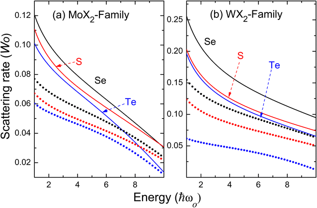 |
| | Fig. 9 Scattering rate as a function of the reduced energy E/ℏωo for the (a) MoX2 and (b) WX2 families. Straight lines represent the ML samples (ωo = ωE′), dots correspond to 2ML materials (ωo = ωEul). The parameters in Tables 1–3 are used, the results are given in units of Wo (20) for the ML parameters. | |
Because the phonon frequencies for the ML and 2ML are very similar for each family, comparing the results for those compounds with the same anion is possible. In all cases, τ−1 is smaller in the bilayer structures. The sequence of values from lowest to highest in the SR seen in Fig. 9 is related to the increase of the ro parameter when passing from the S to Te anion (see Table 3). Fig. 9 for the ML resembles the values obtained in ref. 51.
V. Conclusions
We have performed first principles calculations to examine the phonon dispersion curves for single-layer and bilayers of the MX2 family (M = Mo, W and X = S, Se, Te). The method enables us to examine the parameters describing the phonon dispersion and to elucidate their role on the optical branches. Based on the ab initio results of Fig. 1–3, we report the phonon parameters for the long-wavelength polar vibrations in bilayer TMDs for in-plane and out-of-plane motions. The latter was done by fitting the analytical phonon dispersion laws provided by the macroscopic equations obtained in the framework of the phenomenological continuum limit to the phonon dispersion obtained by first principles calculations. These results allow us to validate the analytical equations reported in Section III as a function of the phonon wave vector for all-optical phonon branches; this is one of the main achievements of this work, graphically represented in Fig. 5–8 together with the set of parameters that describe the twelve dispersion laws (see Table 1). The most significant differences between the single-layer and bilayer results are linked to the polar branches with E-symmetry. Although the phonon parameters for the other modes (polar and non-polar) are very similar, this does not happen with the curvatures of the longitudinal and transverse modes and the increase in the observed slope value Ξ when going from a ML to 2ML (compare Tables 1 and 2). All this is a consequence of the neighborhood influence on the dielectric properties of the 2D TMD. Using first principles analysis, we have derived the Pekar–Fröhlich Hamiltonian in double-layer structures in the small-phonon momentum limit. The analysis provides the strength of the PF interaction for ML (see ref. 52) and 2ML of MoS2, MoSe2, MoTe2, WS2, WSe2 and WTe2 semiconductors.
We have examined the intrinsic transport properties by evaluating the dispersion rate at low carrier density and high temperature. 2ML structures have a longer lifetime than ML ones. We demonstrate that the number of layers is paramount in evaluating the dispersion rate and transport properties. The quantitative picture of the scattering rate displayed in eqn (19) allows us to delineate the critical factors involved in conductivity and mobility. One particularly interesting point is to consider TMD materials in the presence of an external magnetic field where the transport of carriers is spin polarized.59
The reported analytical models become necessary to understand better transport properties, infrared and Raman spectroscopy. Among other topics, the generalization of the present results to the evaluation of optical phonons in 2D Moiré hetero-bilayers offers an attractive field to study the peculiarities of the symmetries of the optical branches, the dispersion laws, how the electron–phonon interaction is modified and the impact that these effects produce on the Raman selection rules, dielectric, optical properties and transport phenomena of these exotic structures.
Appendix A: parameters of ab initio calculations
In the DFPT calculations, the dynamical matrices were computed for a Γ-centered n × n q-point grid in the reciprocal lattice unit cell corresponding to the supercell that contains the ML and 2ML structures. The electron wavefunctions are expanded in plane waves restricted by a kinetic energy cutoff. The electronic density is also expanded in plane waves restricted by a cutoff. For the electronic calculation, the reciprocal unit cell was sampled using a Γ-centered m × m k-point grid. The employed computational parameters for MoX2 and WX2 with X = S, Se and Te are summarized in Table 3 and 4. We observe that for a given TMD family the lattice constant and ro increase as the mass of the chalcogen atom X increases. Furthermore, the screening parameter, or similarly, the in-plane polarizability, doubles its value when moving from the ML to the two-layer. The latter has an important impact on the evaluation of the PF Hamiltonian in eqn (17).
Table 3 Employed parameters for the evaluation of the out-of-plane and in-plane optical phonon dispersion relations of a bilayer of MX2 (M = Mo, W; X = S, Se, Te). The corresponding values for a monolayer are also listed. a – Optimized lattice constant, c – interlayer distance, d – thickness of the monolayer or bilayer, r0 – screening parameter, ε – dielectric constant and m – the electron effective constant
| |
MoS2 |
MoSe2 |
MoTe2 |
WS2 |
WSe2 |
WTe2 |
| Ref. 60. |
| Single-layer |
| a (Å) |
3.1635 |
3.2991 |
3.5274 |
3.1627 |
3.2949 |
3.5230 |
| c (Å) |
15.9300 |
16.4957 |
17.6370 |
15.8137 |
16.4744 |
17.6481 |
| r0 (Å) |
46.0353 |
53.4115 |
68.6629 |
41.9088 |
48.8415 |
64.87084 |
| d (Å) |
5.4816 |
5.9689 |
6.6794 |
5.5108 |
6.0037 |
6.6959 |
| ε |
16.8161 |
17.9151 |
20.5759 |
15.2315 |
16.2908 |
19.3933 |
![[thin space (1/6-em)]](https://www.rsc.org/images/entities/char_2009.gif) |
| Bilayer |
| a (Å) |
3.1647 |
3.3001 |
3.5305 |
3.1831 |
3.2964 |
3.5319 |
| c (Å) |
28.4820 |
29.2058 |
31.1933 |
28.3299 |
29.6674 |
31.7871 |
| r0(Å) |
93.1131 |
107.9929 |
139.0393 |
85.2742 |
98.4814 |
131.1408 |
| d (Å) |
11.0497 |
12.0003 |
13.3737 |
11.0062 |
12.0314 |
13.36 |
| ε |
16.8732 |
18.0168 |
20.8090 |
15.5173 |
16.3910 |
19.6489 |
| m/moa |
0.43 |
0.49 |
0.53 |
0.26 |
0.28 |
0.26 |
Table 4 Parameters used for the ab initio calculations. Wavefunction (wf) and density (rho) cutoffs, k-point, and q-point gridsa
| |
MoS2 |
MoSe2 |
MoTe2 |
WS2 |
WSe2 |
WTe2 |
| The PAW potential files used were Mo.pbe-spn-kjpaw_psl.1.0.0.UPF, W.pbe-spn-kjpaw_psl.1.0.0.UPF, S.pbe-n-kjpaw_psl.1.0.0.UPF, Se.pbe-n-kjpaw_psl.1.0.0.UPF, and Te.pbe-n-kjpaw_psl.1.0.0.UPF from ref. 50. |
| wf cutoff (Ry) |
65 |
80 |
80 |
100 |
80 |
80 |
| rho cutoff (Ry) |
650 |
800 |
800 |
800 |
800 |
800 |
| k-mesh |
12 × 12 |
12 × 12 |
12 × 12 |
12 × 12 |
15 × 15 |
12 × 12 |
| q-mesh |
6 × 6 |
6 × 6 |
6 × 6 |
6 × 6 |
6 × 6 |
6 × 6 |
Appendix B: polar phonon: A2u-symmetry
For the out-of-plane optical vibrations, eqn (4) is complemented by the Maxwell equation| | |
∇·(Ez(ρ,z) + 4πPz(ρ,z)) = 0,
| (B1) |
with Pz being the total macroscopic polarization due to the two sub-cell polarization contributions.
We assume the existence of a polarization field coupling the phonon amplitude with the macroscopic electric field in the plane. The mechanical displacement Uip induces an electric field Eind(Uip), a general expression for the induced field can be taken as Eind = αA2uUip. Thus, for the vector polarization Pz we assume the linear constitutive phenomenological relation
| | |
Pz = [αA2uUip(ρ) + χeEz(ρ,0)]p(z),
| (B2) |
where
χe is the out-of-plane electronic susceptibility
61 and
p(
z) is the polarization density out-of-plane as given by
p(
z) = 1/
d; |
z| <
d/2 and 0 if |
z| >
d/2,
d the thickness of the bilayer. From
eqn (B1) and taking
Ez =
Ez(
ρ,
z) = −∇
φ(
ρ,
z) it follows that
| |
 | (B4) |
Poisson eqn (B3) points out that the electrostatic potential φ(ρ,z) is due to the polarization charge 4π∇·Pz of the polarization field, eqn (B2). Due to the translation symmetry in the plane, we can choose the electrostatic potential and vector amplitude as φ(ρ,z) = ϕ(z)eiq·ρ, Uip = Uoeiq·ρ, respectively. Therefore,  and eqn (B3) reduces to
| |
 | (B5) |
Considering the Fourier transform  from (B5) it follows that
| |
 | (B6) |
The z-component of the electric field Ez(ρ,0) is given by
| |
 | (B7) |
Inserting (B6) into (B7) we obtain
| |
 | (B8) |
In the long wavelength limit e−qd/2 ≈ 1. Therefore,
| |
 | (B9) |
Employing the identity ∇ × ∇ × Uip − ∇(∇·Uip) = −∇2Uip = q2Uip from eqn (4) we obtain
| |
 | (B10) |
and the
ω(
q) for the A
2u mode is equal to
| |
 | (B11) |
The second term on the right side of the above equation renormalizes the intrinsic oscillatory frequency ωA02u
| |
 | (B12) |
thus, the final dispersion relation
eqn (5) for the A
2u mode is obtained.
Appendix C: polar phonon: Eu-symmetry
The total macroscopic electric field E(ρ,z) in the plane satisfies the Maxwell equation| | |
∇·(E(ρ,z) + 4πP(ρ,z)) = 0,
| (C1) |
and for the macroscopic polarization P(ρ,z) we have| | |
P = [αUip(ρ) + α2E(ρ,0)]p(z),
| (C2) |
with α2 the polarizability in the plane. Taking E(ρ,z) = −∇φ(ρ,z) and looking for the solutions as Uip = Uoipeiq·ρ and E(ρ,z = 0) = E(q)eiq·ρ, from eqn (13) and (C1) we have| |
 | (C3) |
and| | |
∇2φ + 4πα2∇ρ2φ(ρ,0)p(z) = 4πα∇·[Uip(ρ)p(z)].
| (C4) |
In (C4), ρpol = 4πα∇·[Uip(ρ)p(z)] is considered as the polarization charge generated by the induced electric field Eind = αUip(ρ). In Poisson’s eqn (C4), the total charge density ρT = ρpol + ρind with
| | |
ρind = −4πα2∇2ρφ(ρ,0)p(z),
| (C5) |
ρind is the induced charge density related to polarization due to the in-plane electric field
E⊥ = −∇
ρφ(
ρ,0) in the bilayer. The presence of an environment leads to a point charge at the origin that creates a field that shields the electrostatic potential
φ(
ρ,
z). For the solution of Poisson’s
eqn (C4), coupled to the mechanical equation of motion
eqn (13), we take the Fourier transform
| |
 | (C6) |
Thus, from (C4) it follows that for the Fourier transform of the electrostatic potential  is
is
| |
 | (C7) |
where the long-wave length limit
qd/2 ≪ 1 was considered and
| |
 | (C8) |
From (C7) and (C8) the Fourier transform of Eρ(ρ,z = 0) = −∇φ(ρ) is given by
| |
 | (C9) |
Considering Uoip = Ul + Ut as the longitudinal and transverse independent components of the vector displacement we obtain the ω(q) laws dictated by eqn (14) and (15).
Appendix D: Pekar–Fröhlich Hamiltonian
Here we discuss the formulation of PF coupling valid for a bilayer of TMD. The lattice vibration, Uip gives rise to the 2D macroscopic electric field E⊥ = −∇ρφ(ρ,0). An electric charge −e is coupled to the scalar potential φ(ρ), so the PF Hamiltonian can be written as| |
ĤPF = −e![[small variant phi, Greek, circumflex]](https://www.rsc.org/images/entities/i_char_e1dc.gif) (ρ). (ρ).
| (D1) |
The polarization charge ρT = ρpol + ρind is responsible for the scalar potential φ as discussed in Appendix C. From eqn (C6) and (C7) immediately follows
| |
 | (D2) |
Transforming the classical field of the phonon amplitude Uip into a quantum-field operator Ûip(ρ) in terms of phonon creation (![[b with combining circumflex]](https://www.rsc.org/images/entities/b_i_char_0062_0302.gif) †q) and annihilation (
†q) and annihilation (![[b with combining circumflex]](https://www.rsc.org/images/entities/b_i_char_0062_0302.gif) q) phonon operator we obtain
q) phonon operator we obtain
| |
 | (D3) |
with
S =
NcA the normalization area,
A the area of the sub-unit cell and
Nc the number of cells. Consequently,
F(
q) →
![[F with combining circumflex]](https://www.rsc.org/images/entities/i_char_0046_0302.gif)
(
q) and
φ(
ρ) →
![[small variant phi, Greek, circumflex]](https://www.rsc.org/images/entities/i_char_e1dc.gif)
(
ρ).
Inserting eqn (D3) into eqn (C8), the in-plane electrostatic potential, eqn (D2), is given by
| |
 | (D4) |
From eqn (D1) and (D4) follows the Hamiltonian, eqn (17).
Conflicts of interest
There are no conflicts to declare.
Acknowledgements
Ab initio calculations were conducted at the following computer centers: CICA (Centro Informático Científico de Andalucía, https://www.cica.es/) and Supercomputing Center Alhambra of Universidad de Granada. ESM acknowledges financial support from ANID-FONDECYT 1221301 and the María Zambrano Program, Ministry of Universities and Seville University, Spain. Powered@NLHPC: this research was partially supported by the supercomputing infrastructure of the NLHPC (ECM-02). G. E. M. and C. T.-G. are grateful for the financial support from the Brazilian agencies, Fundação de Amparo à Pesquisa do Estado de São Paulo (FAPESP: Proc. 2023/10905-2, 2022/08825-8, 2020/07255-8) and Conselho Nacional de Desenvolvimento Científico e Tecnológico (CNPq: Proc. 302007/2019-9).
References
- S. Manzeli, D. Ovchinnikov, D. Pasquier, O. V. Yazyev and A. Kis, Nat. Rev. Mater., 2017, 2, 17033 CrossRef CAS.
- B. Schönfeld, J. J. Huang and S. C. Moss, Acta Crystallogr., Sect. B: Struct. Sci., 1983, 39, 404–407 CrossRef.
- S. Coutinho, M. Tavares, C. Barboza, N. Frazão, E. Moreira and D. L. Azevedo, J. Phys. Chem. Solids, 2017, 111, 25–33 CrossRef CAS.
- Z. Huang, W. Zhang and W. Zhang, Materials, 2016, 9, 716 CrossRef PubMed.
- J. K. Ellis, M. J. Lucero and G. E. Scuseria, Appl. Phys. Lett., 2011, 99, 261908 CrossRef.
- Y. Zhang, T.-R. Chang, B. Zhou, Y.-T. Cui, H. Yan, Z. Liu, F. Schmitt, J. Lee, R. Moore, Y. Chen, H. Lin, H.-T. Jeng, S.-K. Mo, Z. Hussain, A. Bansil and Z.-X. Shen, Nat. Nanotechnol., 2014, 9, 111–115 CrossRef CAS PubMed.
- Z. G. Yu, B. I. Yakobson and Y.-W. Zhang, ACS Appl. Energy Mater., 2018, 1, 4115–4121 CrossRef CAS.
- C. D. English, G. Shine, V. E. Dorgan, K. C. Saraswat and E. Pop, Nano Lett., 2016, 16, 3824–3830 CrossRef CAS PubMed.
- W. Wu, D. De, S.-C. Chang, Y. Wang, H. Peng, J. Bao and S.-S. Pei, Appl. Phys. Lett., 2013, 102, 142106 CrossRef.
- H.-L. Liu, C.-C. Shen, S.-H. Su, C.-L. Hsu, M.-Y. Li and L.-J. Li, Appl. Phys. Lett., 2014, 105, 201905 CrossRef.
- E. Singh, P. Singh, K. S. Kim, G. Y. Yeom and H. S. Nalwa, ACS Appl. Mater. Interfaces, 2019, 11, 11061–11105 CrossRef CAS PubMed.
- S. Rashidi, S. Rashidi, R. K. Heydari, S. Esmaeili, N. Tran, D. Thangi and W. Wei, Progr. Photovolt.: Res. Appl., 2021, 29, 238–261 CrossRef CAS.
- C. Wang, F. Yang and Y. Gao, Nanoscale Adv., 2020, 2, 4323–4340 RSC.
- A. Taffelli, S. Dirè, A. Quaranta and L. Pancheri, Sensors, 2021, 21, 2758 CrossRef CAS PubMed.
- W. Zheng, X. Liu, J. Xie, G. Lu and J. Zhang, Coord. Chem. Rev., 2021, 447, 214151 CrossRef CAS.
- Y. Hu, Y. Huang, C. Tan, X. Zhang, Q. Lu, M. Sindoro, X. Huang, W. Huang, L. Wang and H. Zhang, Mater. Chem. Front., 2017, 1, 24–36 RSC.
- E. C. Ahn, npj 2D Mater. Appl., 2020, 4, 17 CrossRef CAS.
- Y. Liu, N. O. Weiss, X. Duan, H.-C. Cheng, Y. Huang and X. Duan, Nat. Rev. Mater., 2016, 1, 16042 CrossRef CAS.
- A. H. Castro Neto, F. Guinea, N. M. R. Peres, K. S. Novoselov and A. K. Geim, Rev. Mod. Phys., 2009, 81, 109–162 CrossRef CAS.
- E. Suárez Morell, J. D. Correa, P. Vargas, M. Pacheco and Z. Barticevic, Phys.Rev.
B: Condens. Matter Mater. Phys., 2010, 82, 121407 CrossRef.
- Y. Cao, V. Fatemi, S. Fang, K. Watanabe, T. Taniguchi, E. Kaxiras and P. Jarillo-Herrero, Nature, 2018, 556, 43–50 CrossRef CAS PubMed.
- K. Yasuda, X. Wang, K. Watanabe, T. Taniguchi and P. Jarillo-Herrero, Science, 2021, 372, 1458–1462 CrossRef CAS PubMed.
- D. Zhang, P. Schoenherr, P. Sharma and J. Seidel, Nat. Rev. Mater., 2022, 8, 25–40 CrossRef.
- Y. Wang, S. Jiang, J. Xiao, X. Cai, D. Zhang, P. Wang, G. Ma, Y. Han, J. Huang, K. Watanabe, T. Taniguchi, Y. Guo, L. Wang, A. S. Mayorov and G. Yu, Front. Phys., 2022, 17, 43504 CrossRef.
- E. A. Cortés, J. M. Florez and E. S. Morell, J. Phys. Chem. Solids, 2023, 173, 111086 CrossRef.
- X. Wang, K. Yasuda, Y. Zhang, S. Liu, K. Watanabe, T. Taniguchi, J. Hone, L. Fu and P. Jarillo-Herrero, Nat. Nanotechnol., 2022, 17, 367–371 CrossRef CAS PubMed.
- B. Huang, G. Clark, D. R. Klein, D. MacNeill, E. Navarro-Moratalla, K. L. Seyler, N. Wilson, M. A. McGuire, D. H. Cobden, D. Xiao, W. Yao, P. Jarillo-Herrero and X. Xu, Nat. Nanotechnol., 2018, 13, 544–548 CrossRef CAS PubMed.
- E. S. Morell, A. León, R. H. Miwa and P. Vargas, 2D Mater., 2019, 6, 025020 CrossRef CAS.
- H. Li, Z. Yin, Q. He, H. Li, X. Huang, G. Lu, D. W. H. Fam, A. I. Y. Tok, Q. Zhang and H. Zhang, Small, 2012, 8, 63–67 CrossRef CAS PubMed.
- S. Das, H.-Y. Chen, A. V. Penumatcha and J. Appenzeller, Nano Lett., 2013, 13, 100–105 CrossRef CAS PubMed.
- S. Kim, A. Konar, W.-S. Hwang, J. H. Lee, J. Lee, J. Yang, C. Jung, H. Kim, J.-B. Yoo, J.-Y. Choi, Y. W. Jin, S. Y. Lee, D. Jena, W. Choi and K. Kim, Nat. Commun., 2012, 3, 1011 CrossRef PubMed.
- H. Terrones and M. Terrones, J. Mater. Res., 2014, 29, 373–382 CrossRef CAS.
- X. Liu, D. Qu, J. Ryu, F. Ahmed, Z. Yang, D. Lee and W. J. Yoo, Adv. Mater., 2016, 28, 2345–2351 CrossRef CAS PubMed.
- K. M. McCreary, M. Phillips, H.-J. Chuang, D. Wickramaratne, M. Rosenberger, C. S. Hellberg and B. T. Jonker, Nanoscale, 2022, 14, 147–156 RSC.
- G. Fiori, F. Bonaccorso, G. Iannaccone, T. Palacios, D. Neumaier, A. Seabaugh, S. K. Banerjee and L. Colombo, Nat. Nanotechnol., 2014, 9, 768–779 CrossRef CAS PubMed.
- Q. H. Wang, K. Kalantar-Zadeh, A. Kis, J. N. Coleman and M. S. Strano, Nat. Nanotechnol., 2012, 7, 699–712 CrossRef CAS PubMed.
- C. Chakraborty, L. Kinnischtzke, K. M. Goodfellow, R. Beams and A. N. Vamivakas, Nat. Nanotechnol., 2015, 10, 507–511 CrossRef CAS PubMed.
- B. Radisavljevic, A. Radenovic, J. Brivio, V. Giacometti and A. Kis, Nat. Nanotechnol., 2011, 6, 147–150 CrossRef CAS PubMed.
- E. H. Hwang and S. Das Sarma, Phys. Rev. B: Condens. Matter Mater. Phys., 2008, 77, 235437 CrossRef.
- A. Kefayati, J. P. Bird and V. Perebeinos, Phys. Rev. B, 2022, 106, 155415 CrossRef CAS.
- C. Trallero-Giner, D. G. Santiago-Pérez and V. M. Fomin, Sci. Rep., 2023, 13, 292 CrossRef CAS PubMed.
- N. A. Pike, A. Dewandre, B. Van Troeye, X. Gonze and M. J. Verstraete, Phys. Rev. Mater., 2019, 3, 074009 CrossRef CAS.
- I. Paradisanos, G. Wang, E. M. Alexeev, A. R. Cadore, X. Marie, A. C. Ferrari, M. M. Glazov and B. Urbaszek, Nat. Commun., 2021, 12, 538 CrossRef CAS PubMed.
- X. Li, J. T. Mullen, Z. Jin, K. M. Borysenko, M. Buongiorno Nardelli and K. W. Kim, Phys. Rev. B: Condens. Matter Mater. Phys., 2013, 87, 115418 CrossRef.
- J. K. Han, M.-A. Kang, C.-Y. Park, M. Lee, S. Myung, W. Song, S. S. Lee, J. Lim and K.-S. An, Nanotechnology, 2019, 30, 335402 CrossRef CAS PubMed.
- S. Baroni, S. de Gironcoli, A. Dal Corso and P. Giannozzi, Rev. Mod. Phys., 2001, 73, 515–562 CrossRef CAS.
- P. Giannozzi, S. Baroni, N. Bonini, M. Calandra, R. Car, C. Cavazzoni, D. Ceresoli, G. L. Chiarotti, M. Cococcioni, I. Dabo, A. dal Corso, S. de Gironcoli, S. Fabris, G. Fratesi, R. Gebauer, U. Gerstmann, C. Gougoussis, A. Kokalj, M. Lazzeri, L. Martin-Samos, N. Marzari, F. Mauri, R. Mazzarello, S. Paolini, A. Pasquarello, L. Paulatto, C. Sbraccia, S. Scandolo, G. Sclauzero, A. P. Seitsonen, A. Smogunov, P. Umari and R. M. Wentzcovitch, J. Phys.: Condens. Matter, 2009, 21, 395502 CrossRef PubMed.
- J. Klimeš, D. R. Bowler and A. Michaelides, Phys. Rev. B: Condens. Matter Mater. Phys., 2011, 83, 195131 CrossRef.
- T. Thonhauser, S. Zuluaga, C. A. Arter, K. Berland, E. Schröder and P. Hyldgaard, Phys. Rev. Lett., 2015, 115, 136402 CrossRef CAS PubMed.
- A. Dal Corso, Comput. Mater. Sci., 2014, 95, 337–350 CrossRef CAS.
- T. Sohier, M. Calandra and F. Mauri, Phys. Rev. B, 2017, 96, 75448 CrossRef.
- N. Scheuschner, R. Gillen, M. Staiger and J. Maultzsch, Phys. Rev. B: Condens. Matter Mater. Phys., 2015, 91, 235409 CrossRef.
- C. Trallero-Giner, E. Menéndez-Proupin, E. S. Morell, R. Pérez-Álvarez and D. G. Santiago-Pérez, Phys. Rev. B, 2021, 103, 235424 CrossRef CAS.
- X. Zhang, X.-F. Qiao, W. Shi, J.-B. Wu, D.-S. Jiang and P.-H. Tan, Chem. Soc. Rev., 2015, 44, 2757–2785 RSC.
- A. V. Kolobov and J. Tominaga, Two-Dimensional Transition-Metal Dichalcogenides, Springer International Publishing Switzerland, 2016, vol. 239 Search PubMed.
- M. Yamamoto, S. T. Wang, M. Ni, Y.-F. Lin, S.-L. Li, S. Aikawa, W.-B. Jian, K. Ueno, K. Wakabayashi and K. Tsukagoshi, ACS Nano, 2014, 8, 3895–3903 CrossRef CAS PubMed.
- P. Y. Yu and M. Cardona, Fundamentals of Semiconductors, Springer, Berlin Heidelberg, 2010 Search PubMed.
- K. Kaasbjerg, K. S. Thygesen and K. W. Jacobsen, Phys. Rev. B: Condens. Matter Mater. Phys., 2012, 85, 115317 CrossRef.
- J. R. Schaibley, H. Yu, G. Clark, P. Rivera, J. S. Ross, K. L. Seyler, W. Yao and X. Xu, Nat. Rev. Mater., 2016, 1, 16055 CrossRef CAS.
- A. Kormányos, G. Burkard, M. Gmitra, J. Fabian, V. Zólyomi, N. D. Drummond and V. Fal’ko, 2D Mater., 2015, 2, 022001 CrossRef.
- J.-Z. Zhang, AIP Adv., 2020, 10, 045316 CrossRef CAS.
|
| This journal is © The Royal Society of Chemistry 2024 |
Click here to see how this site uses Cookies. View our privacy policy here.  Open Access Article
 *a,
E. Suárez Morell
 ab,
G. E. Marques
 c and
C. Trallero-Giner
 c
c

 (ZO2) and
  (ZO1). The patterns of these modes are shown in Fig. 4, while labels indicate their location in the spectra of Fig. 1–3. For each branch of a ML, there are two normal modes of the 2ML. Hence, we have twelve long-wave optical branches: eight vibrating in-plane with symmetries Eg and Eu and four modes oscillating out-of-plane with symmetries A1g and A2u. Three low-frequency optical modes result from combining acoustical modes from the two layers. These modes are not discussed in this article. The vibration patterns displayed in Fig. 4 allow us to understand some trends in the family. In the normal modes E′′ (Eu, Eg) and
  (A2u, A1g) in the ML (2ML), the anions move, while the cation is at rest. The obtained frequencies of each mode differ in less than 4% between MoX2 and WX2. This can be understood if the interatomic force constants are nearly identical for Mo and W with the same anion. On the other hand, in the modes E′ (Eu, Eg) and
  (A2u, A1g), the cation motion opposes the motion of the anions. As discussed below, this motion is associated with the reduced mass μ given by 1/μ = 1/mM + 1/(2mX). Assuming again that the interatomic force constants do not depend on the cation, the frequency of these modes is proportional to
  . Renormalizing the frequencies of MoX2 modes by the factor
  provides an approximation to the frequencies of WX2. When the anion is changed, rescaling by the reduced mass leads to increased errors, suggesting that the force constants depend more strongly on the nature of the anion than the nature of the cation. Even then, the reduced mass helps to understand another trend. The frequencies in the sulfide monolayers increase in the order E′′, E′,
  ,
,  . However, the order E′,
  is reversed in MoSe2 and the tellurides. For
  frequencies, the atomic mass rescaling factor
  is 0.64 and 0.5 for X = Se and Te, respectively. For the E′ frequencies, the reduced mass scaling factor
  is 0.80 and 0.74 for X = Se and Te, respectively. Hence, the
  frequency decreases more than the E′ frequency due to the mass rescaling factor. Moreover, in the case of WSe2, both
  and E′ become almost degenerate (242 vs. 239 cm−1).


 and
and  are the phenomenological parameters obtained by the phonon dispersion ω(q). Using the solution Uip (Uap) = Uoi(Uoa)eiq·ρ we get


 and
and  are estimated from the dispersion curves and the phonon dispersion law obtained using ab initio calculations for polar and non-polar optical modes. ωδ in cm−1
 and
and  between the two branches, even the sign is not always preserved. These differences are determined mainly by the dielectric properties of the environment. The in-phase displacement Uip creates an in-plane internal electric field that is greatly affected by the dielectric environment (see eqn (14).)
 (ZO1),
  (ZO2), E′ (LO2, TO2), and E′′ (LO1, TO1) phonon symmetries.
 take similar values except for the polar modes of Eg-symmetry. Comparing the phonon dispersion reported in ref. 53 with the data given in Table 2, we observe that the phonon parameters in both cases are almost the same. Due to incorrect manipulation, the results collected in Table 2 of ref. 53 for WTe2 need to be corrected; also, the correct value for MoS2
  .
.


 ,
, 

![[thin space (1/6-em)]](https://www.rsc.org/images/entities/char_2009.gif)

 and eqn (B3) reduces to
 from (B5) it follows that


 is
is


![[small variant phi, Greek, circumflex]](https://www.rsc.org/images/entities/i_char_e1dc.gif) (ρ).
(ρ).

![[b with combining circumflex]](https://www.rsc.org/images/entities/b_i_char_0062_0302.gif) †q) and annihilation (
†q) and annihilation (![[b with combining circumflex]](https://www.rsc.org/images/entities/b_i_char_0062_0302.gif) q) phonon operator we obtain
q) phonon operator we obtain
![[F with combining circumflex]](https://www.rsc.org/images/entities/i_char_0046_0302.gif) (q) and φ(ρ) →
(q) and φ(ρ) → ![[small variant phi, Greek, circumflex]](https://www.rsc.org/images/entities/i_char_e1dc.gif) (ρ).
(ρ).


