DOI:
10.1039/D3RA08866A
(Paper)
RSC Adv., 2024,
14, 7241-7250
Realizing new 2D spintronic materials from the non-magnetic 1T-PdO2 monolayer through vacancy defects and doping
Received
26th December 2023
, Accepted 12th February 2024
First published on 28th February 2024
Abstract
In this work, vacancy- and doping-based magnetism engineering in a non-magnetic 1T-PdO2 monolayer is explored in order to realize new two-dimensional (2D) spintronic materials. The pristine monolayer is an indirect gap semiconductor with a band gap of 1.45 (3.20) eV obtained using the PBE (HSE06) functional. Half-metallicity with a total magnetic moment of 3.95 μB is induced by creating a single Pd vacancy, where the magnetic properties are produced mainly by O atoms around the vacancy site. In contrast, the non-magnetic nature is preserved under the effects of a single O vacancy, however a band gap reduction in the order of 37.93% is achieved. Further doping with transition metals (TMs = V, Cr, Mn, and Fe) in the Pd sublattice and with non-metals (B, C, N, and F) in the O sublattice is investigated. TM impurities lead to the emergence of a diluted magnetic semiconductor nature, where total magnetic moments of 1.00, 2.00, and 3.00 μB are obtained in the V-, Cr(Fe)-, and Mn-doped systems, respectively. In these cases, the TMs’ 3d electrons mainly originate the system’s magnetism. Significant magnetization of the PdO2 monolayer is also achieved by doping with B, N, and F atoms, where either half-metallic or diluted magnetic semiconductor natures are induced. Herein, electronic and magnetic properties are regulated mainly by the interactions between the 2p orbital of the dopant, 4d orbital of the first neighbor Pd atoms, and 2p orbital of the second neighbor O atoms. Meanwhile, C impurity induces no magnetism in the PdO2 monolayer because of the strong electronic hybridization with their neighbor atoms. Results presented herein may introduce efficient approaches to engineer magnetism in a non-magnetic PdO2 monolayer, such that the functionalized systems are further recommended for prospective spintronic applications.
1. Introduction
Since the discovery of graphene,1 two-dimensional (2D) materials have started to attract great attention from scientific community. Being the thinnest and strongest material discovered until now, graphene has been the most explored 2D material and has exceptional properties such as zero effective mass, high intrinsic carrier mobility, high thermal conductivity, and large traveling distances (μm) without scattering at room temperature.2,3 However, the absence of an intrinsic band gap presents a challenging limitation, but not limited to, of graphene for practical applications. Therefore, searching for new alternative 2D materials has been undertaken by the worldwide research community. So far, a large variety of 2D materials, including insulator,4,5 semiconductor,6,7 superconductor,8,9 and metallic members,10,11 have been discovered. Of them, 2D transition metal dichalcogenides (TMDs; MX2, X = S, Se) have gained great research interest because of their interesting and easily tunable electronic, optical, and catalytic properties.12–14 Such that they hold promise for applications in gas sensors,15,16 transistor devices,17,18 and high speed photodetection,19,20 and so on. The most investigated 2D TMDs are Mo- and W-dichalcogenides,21,22 and Zr- and Hf-dichalcogenides,23,24 meanwhile the Pd-dichalcogenides have received less attention. Various researchers have explored the electronic and optical properties of the PdS2 and PdSe2 monolayers, as well as the Janus PdSSe structure.25,26 It has been found that these are semiconductor 2D materials with relatively large intrinsic band gaps. Many 2D metal oxides have been investigated theoretically or synthesized experimentally,27,28 and there are the questions of whether the PdO2 monolayer will be stable and what properties does this 2D material hold?
On the other hand, the rapid growth of advanced information technology requires smaller and faster semiconductor devices, such that Moore's law is no longer true because of the miniaturization of transistors. However, increasing the number of transistors brings with it power consumption issues. Therefore, searching for alternative solutions is essential. As an emerging field for future nanoelectronic devices, spintronics (or spin-based electronics) not only reduces the energy consumption but also has a great advantage of voluminous memory and fast processing performance.29,30 In spintronic devices, the electron spin is considered as an additional degree of freedom, such that the generation of spin current is crucial. Therefore developing highly spin-polarized materials is very important for the spintronic performance. In this regard, half-metallic and diluted magnetic semiconductor materials hold promise for spintronic applications thanks to their 100% spin polarization.31,32 For many years, different bulk systems, such as Heusler compounds,33,34 diluted magnetic semiconductors,35,36 metal oxides,37,38 and double perovskites,39,40 have been investigated. Recently, researchers have switched attention to explore 2D materials for spintronic applications. However, very few of these materials have intrinsic magnetism in their pristine form, therefore different methods have been proposed to get appropriate magnetization, such as creating vacancies41,42 and doping with magnetic impurities (transition metals) and non-metals.43,44
Nowadays, researchers have paid much attention to discovering new 2D materials with two or more functions to fabricate multifunctional devices.45 Motivated by the recent research effort to develop new spintronic 2D materials, the main aim of this work is to propose efficient approaches to realize new highly spin-polarized materials from the PdO2 monolayer. There are very few works reporting about this 2D material. Recently, Wani et al.46 have predicted promising thermoelectric performance for the PdO2 monolayer. Results indicate its semiconductor nature with a band gap of 1.40 eV. In this work, the stability as well as electronic properties and chemical bond of PdO2 monolayer are systematically investigated. Further, effects of a single Pd vacancy and O vacancy are considered. In addition, doping with transition metals in the Pd sublattice and with non-metals in the O sublattice is also explored. It is anticipated that feature-rich electronic and magnetic properties can be induced in the PdO2 monolayer, such that the defected and doped PdO2 systems are introduced for spintronic applications. Experimentally, these systems can be realized by atom/ion bombardment, which has been widely utilized for the defect engineering and doping of 2D materials.47,48
2. Computational details
Based on density functional theory (DFT),49 spin-polarized first-principles calculations are carried out to investigate the pristine, vacancy-defected, and doped PdO2 monolayer. The projector augmented wave (PAW) as implemented in the Vienna ab initio simulation package (VASP)50,51 is employed to treat the interactions between ion cores and valence electrons. In the Perdew–Burke–Ernzerhof (PBE) parameterization,52 the generalized gradient approximation (GGA-PBE) is employed to consider the electron exchange–correlation potential. The HSE06 hybrid functional is also utilized in order to get a more accurate band gap prediction of the PdO2 monolayer,53 which includes 25% fraction of the exact Hartree exchange potential (parameter AEXX = 0.25) and a range-separation parameter HFSCREEN = 0.2 Å−1. In addition, the GGA+U approach by Dudarev54 is adopted to describe the correlation effects of the 3d electrons of V, Cr, Mn, and Fe transition metals with Ueff values of 3.25, 3.70, 3.90, and 5.40 eV, respectively, which have been successfully employed by several research groups.55 The plane wave basis set is truncated by a cutoff energy of 500 eV. The convergence criteria for energy and force are set to 1 × 10⁻⁶ eV and 1 × 10⁻² eV Å−1, respectively. k-grids are generated within the framework of the Γ-centered Monkhorst–Pack method,56 where the unit cell and supercell are sampled with 20 × 20 × 1 and 4 × 4 × 1 mesh, respectively. To model the defected and doped systems, a 4 × 4 × 1 supercell of the PdO2 monolayer is generated, which contains 48 atoms (16 Pd atoms and 32 O atoms). This supercell provides a reasonable system size that guarantees negligible interactions between dopant images. In all cases, a vacuum region wider than 14 Å is inserted along the z-direction to get negligible interactions between perpendicularly periodic layers.
3. Results and discussion
3.1. Stability and electronic properties of PdO2 monolayer
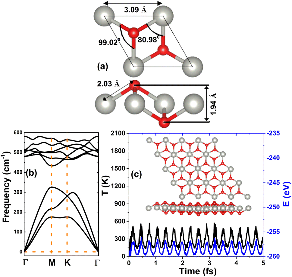
Fig. 1a shows the optimized unit cell of the PdO2 monolayer in the 1T structure. Note that the structure is centrosymmetric, built up from [PdO6] octahedral motifs. From the side-view, three separated atomic planes in the order O–Pd–O can be noted. From the structural optimization, the following parameters are obtained to describe the PdO2 monolayer unit cell: (a) lattice constant a = 3.09 Å; (b) chemical bond length dPd–O = 2.03 Å; (c) interatomic angles ∠PdOPd = 99.02° and ∠OPdO = 80.98°; and (d) total buckling height ΔO–O = 2 × ΔO–Pd = 2 × 0.97 = 1.94 Å. It is worth mentioning that the lattice constant and chemical bond lengths are smaller than those of the PdS2 and PdSe2 monolayers,57 suggesting the reasonability of our results since these parameters increase according to the increase in the atomic number of the VIA-group atoms (that is, the increase in atomic size). Before investigating the ground state properties of the PdO2 monolayer, its stability is verified as follows:
• Elastic constants are calculated to determine the mechanical stability, herein the elasticity of the hexagonal structure is characterized by C11 and C12 constants. According to our calculations, these constants have values of 119.44 and 28.35 N m−1, respectively. Note that Born's criteria (C11 > 0 and C11 > C12)58 are satisfied, indicating that the PdO2 monolayer is mechanically stable.
• On the basis of phonon calculations, the dynamical stability is determined. The calculated phonon spectra given in Fig. 1b reveal that none of three low-frequency acoustic modes and all the six high-frequency optical modes exhibit imaginary frequencies, implying that the PdO2 monolayer is dynamically stable.
• AIMD simulations are carried out to examine the thermal stability. Results in Fig. 1c assert that the initial structural configuration of the PdO2 monolayer is well preserved despite a small vibration of the constituent atoms around their equilibrium sites, where none of the chemical bonds are broken. These results indicate that the PdO2 monolayer is thermally stable.
 |
| | Fig. 1 (a) Optimized atomic structure (Pd: grey ball; O: red ball), (b) phonon dispersion curves, and (c) AIMD simulations at 300 K (inset: atomic structure after 5 fs) of the PdO2 monolayer. | |
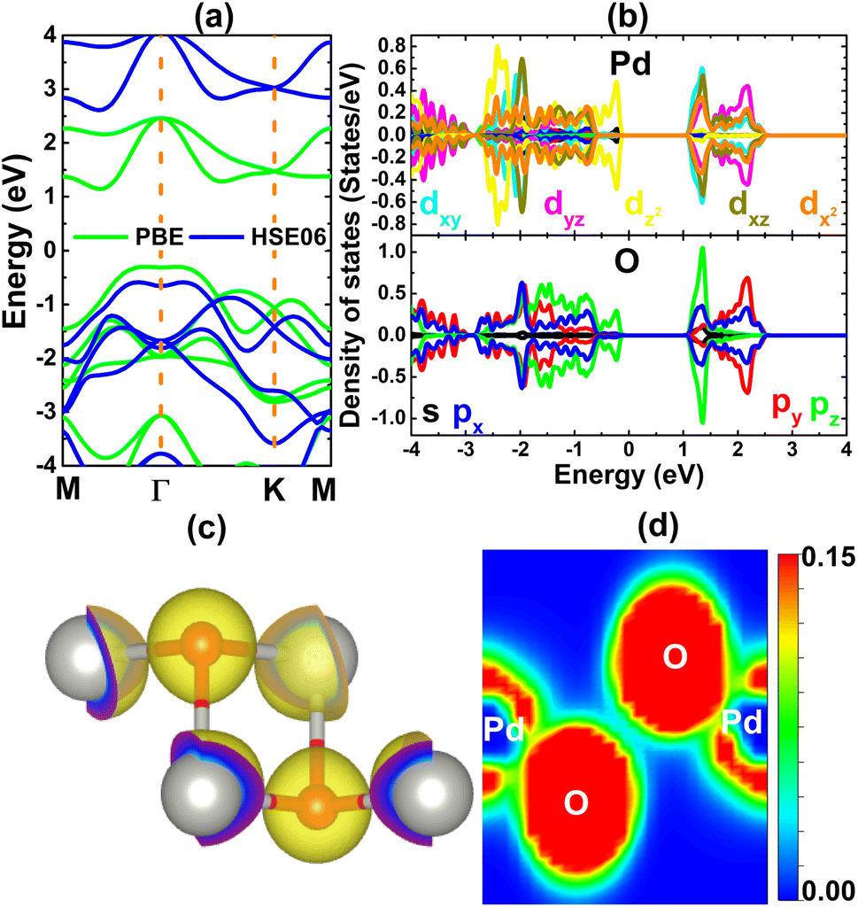
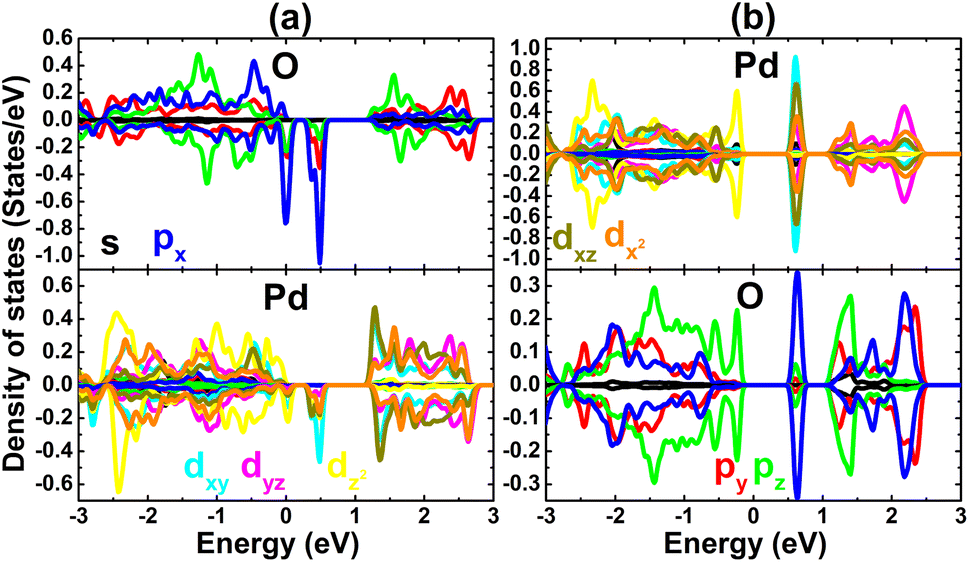
Having confirmed good stability of the PdO2 monolayer, the study is shifted to the analysis of its electronic properties and chemical bonds. The band structure displayed in Fig. 2a asserts the indirect gap semiconductor nature of this 2D material, where PBE- and HSE06-based calculations yield band gaps of 1.45 and 3.20 eV, respectively. Since a band gap underestimation is normally obtained with the standard PBE functional, the HSE06-based band gap is expected to be more accurate considering the inclusion of 25% fraction of the exact Hartree potential.53 The band structure is formed mainly by Pd-4d and O-2p orbitals as observed in the projected density of states (PDOS) spectra given in Fig. 2b. Note that the upper part of the valence band is originated mainly from Pd-dz2 and O-pz states, while the lower part of the conduction band is built up mainly from Pd-dxy-dxz-dx2 and O-pz states. The PDOS profile suggests significant electronic hybridization between Pd-4d and O-2p orbitals, consequently covalent chemical bonds are formed. This feature is confirmed by the valence charge distribution in Fig. 2c, where a large charge distribution is observed in the bridge positions. However, the charge distribution is mostly directional to O atoms, which may be a consequence of the more electronegative nature of the O atom in comparison with the Pd atom. Therefore, the ionic character should not be neglected in the PdO2 monolayer, which may be generated by the charge transfer process. Quantitatively, the Bader charge analysis implies that each Pd atom transfers a charge quantity of 1.30e to two O atoms (each O atom receives 0.65e). This process is also confirmed in the electron localization functional illustrated in Fig. 2d, where large localization is centered at O sites. Therefore, it can be concluded that the chemical bonds in the PdO2 monolayer are a mix of covalent and ionic characters.
 |
| | Fig. 2 (a) Electronic band structure (the Fermi level is set to 0 eV), (b) projected density of states, (c) charge distribution (iso-surface value: 0.15 e Å−3), and (d) electron localization function of the PdO2 monolayer. | |
3.2. Effects of single vacancy
In this part, the effects of single vacancies in the PdO2 monolayer are investigated. Firstly, the formation energy of the defect Ef is calculated as follows:where Eds and Epm are the total energy of the defected and perfect monolayer, respectively; μX refers to the chemical potential of the X atom (X = Pd or O). According to our simulations, Ef values of 4.74 and 1.68 eV are obtained for a single Pd vacancy and single O vacancy (see Table 1). Note that the creation of a single Pd vacancy requires supplying larger energy than for a single O vacancy. Then, the cohesive energy of the defected systems Ec is calculated to examine their stability using the following formula:| |
 | (2) |
EX and nX denote the energy of an isolated X atom and number of X atoms in the system, respectively. Negative Ec values of −3.87 and −3.95 eV per atom are obtained for the PdO2 monolayer with a single Pd vacancy and single O vacancy, respectively. These results indicate that the defected systems are structurally and chemically stable, where the creation of single vacancies does not break the chemical bonds. However, it is worth mentioning that the single Pd vacancy may reduce slightly the stability considering that the Ec value becomes less negative than that of the perfect PdO2 monolayer (−3.97 eV per atom).
Table 1 Formation/doping energy Ef/Ed (eV), cohesive energy Ec (eV per atom), electronic band gap Eg (eV; spin-up/spin-down; M: metallic), charge transferred from impurity ΔQ (e; “−”: charge gain; “+”: charge loss) and total magnetic moment Mt (μB) of the defected/doped PdO2 monolayers
| |
Ef/Ed |
Ec |
Eg |
ΔQ |
Mt |
| VaPd |
4.74 |
−3.87 |
1.39/M |
— |
3.95 |
| VaO |
1.68 |
−3.95 |
0.90/0.90 |
— |
0.00 |
| VPd |
−5.57 |
−4.08 |
0.98/1.33 |
+1.94 |
1.00 |
| CrPd |
−5.07 |
−4.01 |
0.73/1.33 |
+1.81 |
2.00 |
| MnPd |
−3.91 |
−4.01 |
1.33/1.34 |
+1.76 |
3.00 |
| FePd |
−2.57 |
−4.02 |
0.92/1.35 |
+1.59 |
2.00 |
| BO |
3.18 |
−3.97 |
1.43/M |
+0.82 |
0.98 |
| CO |
4.08 |
−3.99 |
0.93/0.93 |
−0.07 |
0.00 |
| NO |
3.10 |
−3.95 |
1.43/0.47 |
−0.47 |
1.00 |
| FO |
−0.38 |
−3.94 |
0.32/1.16 |
−0.57 |
1.00 |
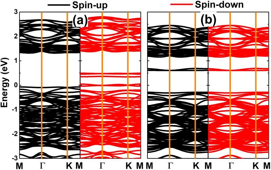
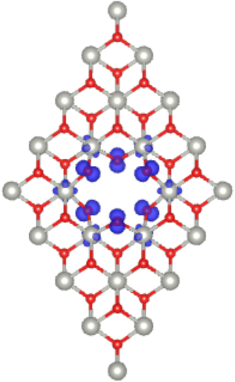
Fig. 3 shows the spin-polarized band structure (BS) of the vacancy-defected PdO2 monolayer. Note that the Pd single vacancy breaks the spin symmetry around the Fermi level, where new middle-gap states emerge. The BS profiles indicate the semiconductor spin-up state with a band gap of 1.39 eV and metallic spin-down state. Such that, the creation of a single Pd vacancy can be suggested as an efficient approach to induce half-metallicity in the PdO2 monolayer, which is desirable for spintronic applications.32 In contrast, the band structure is spin-symmetric without any spin polarization in the case of the single O vacancy. In this case, new middle-gap states appear above the Fermi level to reduce the electronic band gap of the PdO2 monolayer. Specifically, an energy gap of 0.90 eV is obtained, which corresponds to a reduction in the order of 37.93% from that of the perfect monolayer. Analyzing the BS spin polarization, there can be expected significant magnetism in the PdO2 monolayer induced by creating a single Pd vacancy. This feature is further confirmed by a total magnetic moment of 3.95 μB and the spin density as illustrated in Fig. 4. Note that spin density surfaces are centered mainly at O atoms closest to the vacancy Pd site, indicating the key role of these atoms in producing the magnetic properties of the defected PdO2 monolayer.
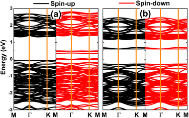 |
| | Fig. 3 Spin-polarized band structure (the Fermi level is set to 0 eV) of the PdO2 monolayer with (a) single Pd vacancy and (b) single O vacancy. | |
 |
| | Fig. 4 Spin density (iso-surface value: 0.02 e Å−3) in the PdO2 monolayer with a single Pd vacancy. | |
PDOS spectra of the first and second atoms from vacancy sites in the PdO2 monolayer are displayed in Fig. 5. In the case of the single Pd vacancy, the middle gaps are derived mainly from O-px,y states with a small contribution from the Pd-dxy state. The spin polarization suggests that the magnetism is originated mainly from the O-px,y state. On the other hand, a single O vacancy induces new middle-gap states to reduce the electronic band gap that are formed mainly by px,y states of the second neighbor O atoms from the vacancy site. Therefore, the atoms around defect sites generate the band structure around the Fermi level, consequently they determine mainly the electronic and magnetic properties of the defected PdO2 monolayer.
 |
| | Fig. 5 Projected density of states of first and second atoms from the vacancy site in the PdO2 monolayer with (a) single Pd vacancy and (b) single O vacancy. | |
3.3. Effects of doping with transition metals
Herein, the effects of doping with transition metal (TMs = V, Cr, Mn, Fe) in the Pd sublattice in the PdO2 monolayer are investigated. The doping energy Ed is calculated as follows:| | |
Ed = Edos − Epm + μPd − μD
| (3) |
where Edos and Epm are the total energy of the doped and perfect monolayer, respectively; μPd and μD refer to the chemical potential of Pd and the transition metal, respectively. Then the structural–chemical stability of the doped systems is verified through the cohesive energy Ec, which is calculated using the following expression:| |
 | (4) |
EX and nX denote the energy of an isolated X atom and number of X atoms in the system, respectively. Results are given in Table 1. The obtained Ed values for V, Cr, Mn, and Fe dopants are −5.57, −5.07, −3.91, and −2.57 eV, respectively. The negative Ed values suggest an exothermic doping process for transition metals in the PdO2 monolayer, where the degree of difficulty may increase according to the increase in the atomic number of the TM impurities since this parameter becomes more positive in this direction. Once formed, all the TM-doped systems exhibit good structural–chemical stability since their cohesive energy has negative values between −4.08 and −4.01 eV per atom, which are slightly more negative than that of the bare monolayer (−3.97 eV per atom).
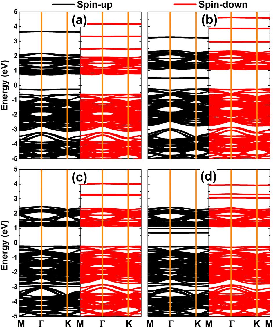
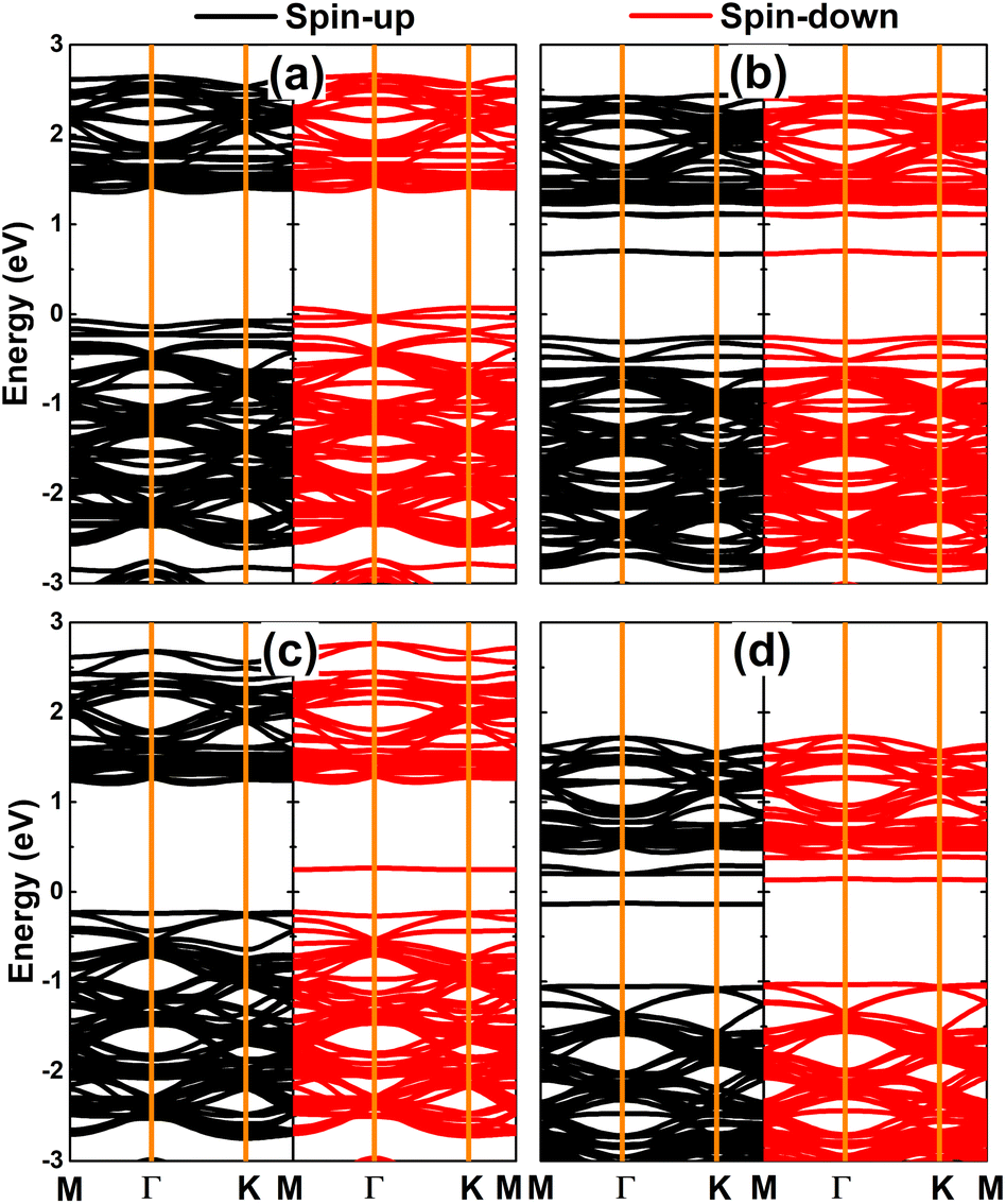
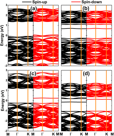
Fig. 6 shows the spin-polarized band structures of V-, Cr-, Mn-, and Fe-doped PdO2 monolayers. Significant spin polarization around the Fermi level and in the upper part of the conduction band can be noted, where new middle-gap flat energy branches are observed in both spin channels. Moreover, the semiconductor character is preserved in both spins of the PdO2 monolayer upon doping with transition metals. The spin-up/spin-down energy gaps of the V-, Cr-, Mn-, and Fe-doped system are 0.98/1.33, 0.73/1.33, 1.33/1.34, and 0.92/1.35 eV, respectively. These results indicate the emergence of the diluted magnetic semiconductor nature, such that the incorporation of magnetic TM impurities in the PdO2 monolayer may be introduced as an effective method to make new 2D spintronic materials.32 Using the Bader charge analysis, it is found that V, Cr, Mn, and Fe impurities lose charge transferring charge amounts of 1.94, 1.81, 1.76, and 1.59e to the host monolayer, respectively. Undoubtedly charge loss is a characteristic of metals (low electronegative atoms) in compound materials.
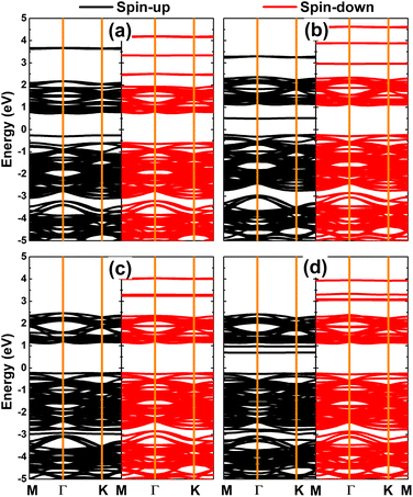 |
| | Fig. 6 Spin-polarized band structures (the Fermi level is set to 0 eV) of (a) V-, (b) Cr-, (c) Mn-, and (d) Fe-doped PdO2 monolayers. | |
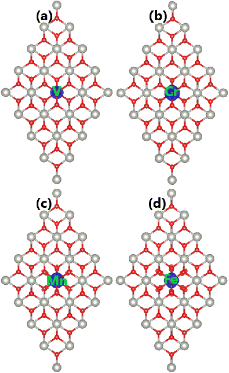
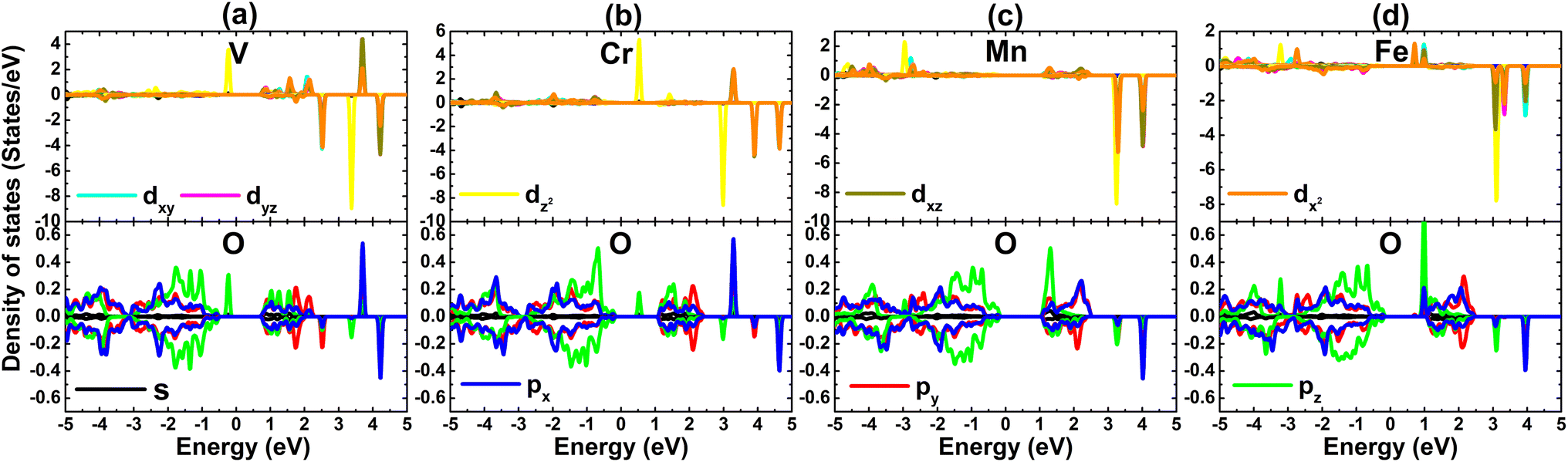
The spin polarization in Fig. 6 suggests that PdO2 is significantly magnetized by doping with transition metals. It is found that the charge distribution between spin channels is different, which is reflected in the total magnetic moments of 1.00, 2.00, and 3.00 μB for V-, Cr(Fe)-, and Mn-doped systems, respectively. The spin density is visualized in Fig. 7. From the figure, one can conclude that magnetic properties of the TM-doped PdO2 monolayer are produced mainly by TM impurities since spin surfaces are centered mainly at their sites. To further investigate the contribution of TM dopants, their PDOS are given in Fig. 8 along with neighbor O atoms. Note that new flat energy branches (in the band structures) are built up mainly from TM-3d states with strong spin polarization, indicating that TM-3d electrons originate mainly the magnetism and regulate the electronic properties of the doped systems. In the considered energy range from −5 to 5 eV, a small contribution from O-2p states is also noted that exhibits a slight hybridization with TM-3d states. However, the interactions between TM impurities and their neighbor O atoms are predominantly ionic due to the charge transfer as analyzed above.
 |
| | Fig. 7 Spin density (iso-surface value: 0.02 e Å−3) in (a) V-, (b) Cr-, (c) Mn-, and (d) Fe-doped PdO2 monolayers. | |
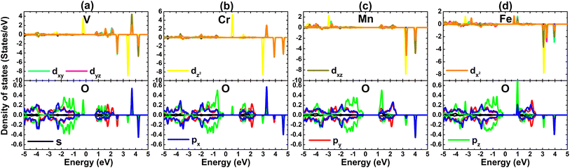 |
| | Fig. 8 Projected density of states of TM impurities and their neighbor O atom in (a) V-, (b) Cr-, (c) Mn-, and (d) Fe-doped PdO2 monolayers. | |
3.4. Effects of doping with non-metal atoms
Now, the effects of doping with non-metal (B, C, N, and F) atoms in the O sublattice in the PdO2 monolayer are investigated. Applying eqn (3) (modified for the O sublattice) and eqn (4), doping energy and cohesive energy are calculated. Results are listed in Table 1. Note that B, C, and N doping are endothermic processes requiring additional energy of 3.18, 4.08, and 3.10 eV, respectively. Meanwhile, exothermic F doping is suggested by the negative Ed value of −0.38 eV. Once formed, all the doped 2D PdO2 systems are structurally–chemically stable considering their negative Ec values between −3.99 and −3.94 eV per atom.
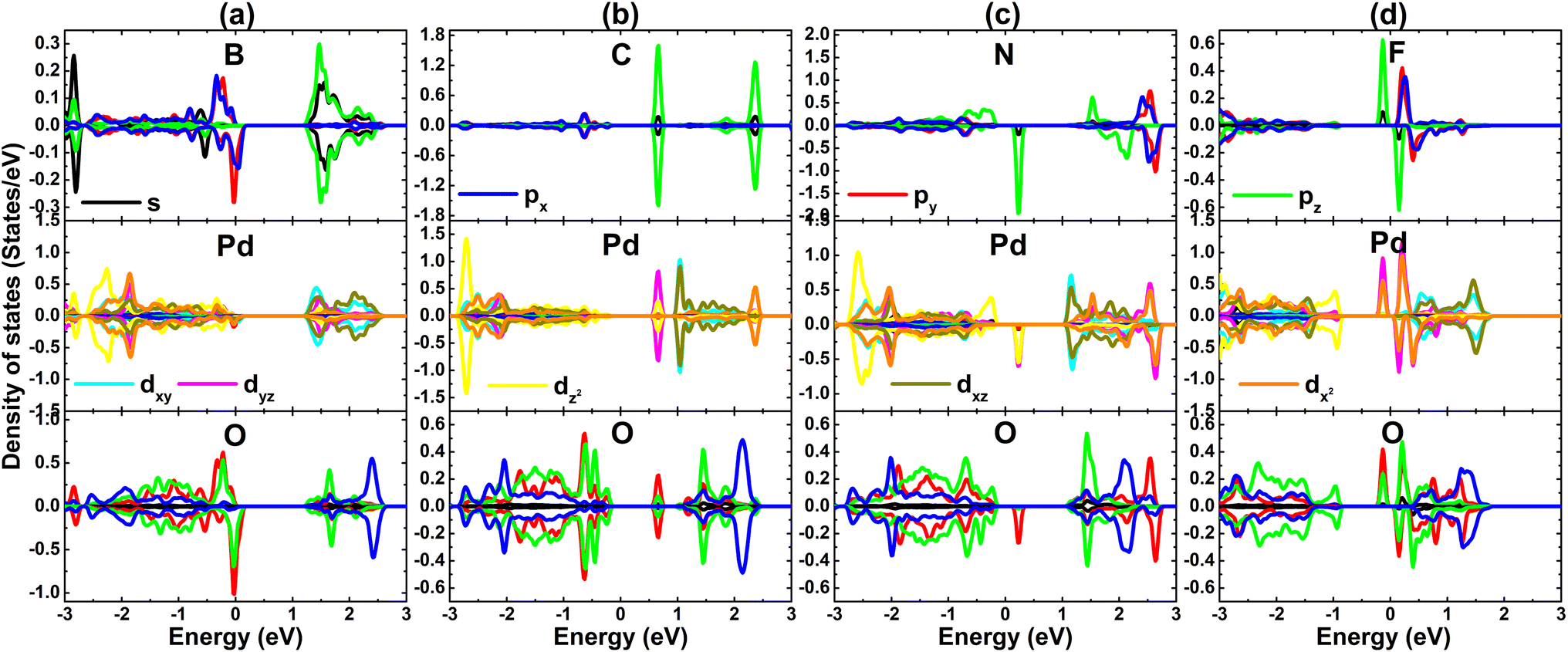
The spin-polarized band structures of PdO2 monolayers doped with non-metal atoms are displayed in Fig. 9. Note that B, N, and F doping breaks the spin symmetry with the appearance of new middle-gap energy states. BS profiles indicate the semiconductor spin-up state and metallic spin-down state of the B-doped system, that is a half-metallic nature is induced. Besides, both spin states exhibit semiconductor behavior, indicating that the N- and F-doped systems are diluted magnetic semiconductor 2D materials. The spin-up/spin-down for these three systems are 1.43/M, 1.43/0.47, and 0.32/1.16 eV, respectively. These features indicate prospective spintronic applicability of the PdO2 monolayer functionalized by doping with B, N, and F atoms. Similarly, new energy states emerge also as a consequence of doping with C atom, however the band structure lacks spin polarization. In this case, the appearance of a flat energy branch above the Fermi level reduces the PdO2 monolayer band gap to 0.93 eV, corresponding to a reduction in the order of 35.86%. Analyzing the Bader charge of impurities, it is found that the B atom acts as a charge loser transferring a charge quantity of 0.82e to the host monolayer. Meanwhile, C, N, and F impurities play the role of a charge gainer receiving 0.07, 0.47, and 0.57e from the host monolayer, respectively. Note that the transferred charge quantity between the C dopant and the host monolayer is quite small, which may be the reason for the absence of spin polarization in the C-doped PdO2 monolayer.
 |
| | Fig. 9 Spin-polarized band structures (the Fermi level is set to 0 eV) of (a) B-, (b) C-, (c) N-, and (d) F-doped PdO2 monolayers. | |
From the BS spin polarization, an unbalanced charge distribution between spin channels in the PdO2 monolayer can be expected, caused by doping with B, N, and F atoms. Such that total magnetic moments of 0.98, 1.00, and 1.00 μB are obtained, indicating that significant magnetization has been achieved. The visualization of spin density in Fig. 10 indicates that the B-doped system magnetism is produced mainly by the second neighbor O atoms from the doping site, suggesting that these O atoms attract charge from both Pd and B atoms. This feature explains why the B impurity acts as a charge loser, despite being incorporated in the O sublattice. On the other hand, the non-metal dopant, the first neighbor Pd atoms and the second neighbor O atoms make contributions to the magnetic properties of the N- and F-doped systems. Since the doping-induced modifications of the electronic interactions in the PdO2 monolayer take place mainly around the doping site, PDOS spectra of the mentioned dopant, and their first and second neighbor atoms are given in Fig. 11 to get more insights into the electronic and magnetic properties. The spin-down metallization in the B-doped system can be attributed mainly to O-py-pz states, which are also responsible for producing the magnetic properties due to their strong spin polarization around the Fermi level. Meanwhile, the hybridization between C-pz and Pd-dyz states generates the flat energy branch above the Fermi level to reduce the energy gap as analyzed above. Moreover, the electronic and magnetic properties of the N- and F-doped systems are also regulated mainly by the interactions between N(F)-2p, Pd-4d, and O-2p orbitals since they exhibit an important presence in the vicinity of the Fermi level, generating new middle-gap states.
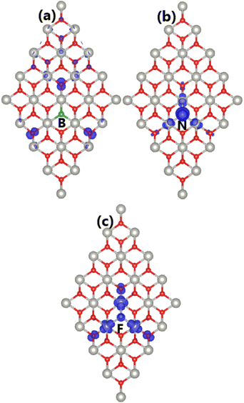 |
| | Fig. 10 Spin density (iso-surface value: 0.005 e Å−3) in (a) B-, (b) N-, and (c) F-doped PdO2 monolayers. | |
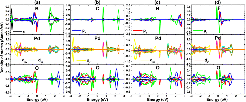 |
| | Fig. 11 Projected density of states of impurities and their neighbor Pd and O atoms in (a) B-, (b) C-, (c) N-, and (d) F-doped PdO2 monolayers. | |
4. Conclusions
In summary, the effects of vacancies and doping (with transition metals in the Pd sublattice and with non-metals in the O sublattice) on the PdO2 monolayer’s electronic and magnetic properties have been systematically investigated using first-principles calculations. The pristine monolayer exhibits good mechanical, dynamical, and thermal stability. Calculations assert also its indirect gap semiconductor nature and reveal a mix of covalent and ionic characters in the Pd–O chemical bond. The monolayer is magnetized by a single Pd vacancy with a half-metallic nature, meanwhile a single O vacancy preserves the non-magnetic semiconductor behavior. Doping with transition metals (V, Cr, Mn, and Fe) and with F atoms is an exothermic process as suggested by the negative doping energy. In contrast, the positive doping energy values may suggest an endothermic process for B, C, and N doping. However, all the doped systems have good structural–chemical stability once formed. 3d electrons of TM impurities generate significant magnetism in the PdO2 monolayer with total magnetic moments between 1.00 and 3.00 μB, where the diluted magnetic semiconductor nature is induced. Herein, the transition metal acts as a charge loser, transferring charge to the host monolayer. The half-metallic and magnetic semiconductor behaviors are also induced by B- and N-, F-doping, respectively. In these cases, total magnetic moments between 0.98 and 1.00 μB are obtained, where the magnetic properties are produced mainly by the impurity, and their first neighbor Pd atoms and second neighbor O atoms. Meanwhile, C doping reduces the PdO2 monolayer band gap without inducing magnetism. Because of the charge attraction of the second atoms, the B impurity acts as a charge loser. In contrast, C, N and F impurities play the role of charge gainer receiving charge from the host monolayer. Results show that feature-rich electronic and magnetic properties can be induced in a non-magnetic PdO2 monolayer, which are suitable for spintronic applications. Therefore, vacancies and doping can be proposed as efficient and solid ways to realize new 2D spintronic materials from a non-magnetic PdO2 monolayer.
Data availability
Data related to this study are available upon reasonable request.
Conflicts of interest
The authors declare that they have no known competing financial interests or personal relationships that could have appeared to influence the work reported in this paper.
Acknowledgements
Calculations were performed in the DGCTIC-UNAM Supercomputing Center (projects LANCAD-UNAM-DGTIC-368) and the high-performance computing cluster (HPCC) of Thu Dau Mot University (TDMU). D. M. Hoat expresses their gratitude to all the valuable support from Duy Tan University, which is going to celebrate its 30th anniversary of establishment (Nov. 11, 1994–2024) towards “Integral, Sustainable and Stable Development”.
References
- K. S. Novoselov, A. K. Geim, S. V. Morozov, D.-e. Jiang, Y. Zhang, S. V. Dubonos, I. V. Grigorieva and A. A. Firsov, Electric field effect in atomically thin carbon films, Science, 2004, 306(5696), 666–669 CrossRef CAS PubMed.
- C. Soldano, A. Mahmood and E. Dujardin, Production, properties and potential of graphene, Carbon, 2010, 48(8), 2127–2150 CrossRef CAS.
- M. J. Allen, V. C. Tung and R. B. Kaner, Honeycomb carbon: a review of graphene, Chem. Rev., 2010, 110(1), 132–145 CrossRef CAS PubMed.
- H. Zhang, M. Holbrook, F. Cheng, H. Nam, M. Liu, C.-R. Pan, D. West, S. Zhang, M.-Y. Chou and C.-K. Shih, Epitaxial growth of two-dimensional insulator monolayer honeycomb BeO, ACS Nano, 2021, 15(2), 2497–2505 CrossRef CAS PubMed.
- K. K. Kim, A. Hsu, X. Jia, S. M. Kim, Y. Shi, M. Hofmann, D. Nezich, J. F. Rodriguez-Nieva, M. Dresselhaus and T. Palacios, et al., Synthesis of monolayer hexagonal boron nitride on Cu foil using chemical vapor deposition, Nano Lett., 2012, 12(1), 161–166 CrossRef PubMed.
- J. Gusakova, X. Wang, L. L. Shiau, A. Krivosheeva, V. Shaposhnikov, V. Borisenko, V. Gusakov and B. K. Tay, Electronic properties of bulk and monolayer TMDs: theoretical study within DFT framework (GVJ-2e method), Phys. Status Solidi A, 2017, 214(12), 1700218 CrossRef.
- S. Tongay, D. S. Narang, J. Kang, W. Fan, C. Ko, A. V. Luce, K. X. Wang, J. Suh, K. D. Patel and V. Pathak, et al., Two-dimensional semiconductor alloys: Monolayer Mo1−xWxSe2, Appl. Phys. Lett., 2014, 104(1), 012101 CrossRef.
- J. Li, P. Song, J. Zhao, K. Vaklinova, X. Zhao, Z. Li, Z. Qiu, Z. Wang, L. Lin and M. Zhao, et al., Printable two-dimensional superconducting monolayers, Nat. Mater., 2021, 20(2), 181–187 CrossRef CAS PubMed.
- H. Wang, X. Huang, J. Lin, J. Cui, Y. Chen, C. Zhu, F. Liu, Q. Zeng, J. Zhou and P. Yu, et al., High-quality monolayer superconductor NbSe2 grown by chemical vapour deposition, Nat. Commun., 2017, 8(1), 394 CrossRef PubMed.
- B. Feng, J. Zhang, R.-Y. Liu, T. Iimori, C. Lian, H. Li, L. Chen, K. Wu, S. Meng and F. Komori, et al., Direct evidence of metallic bands in a monolayer boron sheet, Phys. Rev. B, 2016, 94(4), 041408 CrossRef.
- X. Wan, E. Chen, J. Yao, M. Gao, X. Miao, S. Wang, Y. Gu, S. Xiao, R. Zhan and K. Chen, et al., Synthesis and characterization of metallic Janus MoSH monolayer, ACS Nano, 2021, 15(12), 20319–20331 CrossRef CAS PubMed.
- M. Bernardi, C. Ataca, M. Palummo and J. C. Grossman, Optical and electronic properties of two-dimensional layered materials, Nanophotonics, 2017, 6(2), 479–493 Search PubMed.
- R. Yang, Y. Fan, Y. Zhang, L. Mei, R. Zhu, J. Qin, J. Hu, Z. Chen, Y. Hau Ng and D. Voiry, et al., 2D transitionmetal
dichalcogenides for photocatalysis, Angew. Chem., Int. Ed., 2023, 62(13), e202218016 CrossRef CAS PubMed.
- Z. Guan, S. Ni and S. Hu, Tunable electronic and optical properties of monolayer and multilayer Janus MoSSe as a photocatalyst for solar water splitting: a first-principles study, J. Phys. Chem. C, 2018, 122(11), 6209–6216 CrossRef CAS.
- W. Zheng, X. Liu, J. Xie, G. Lu and J. Zhang, Emerging van der Waals junctions based on TMDs materials for advanced gas sensors, Coord. Chem. Rev., 2021, 447, 214151 CrossRef CAS.
- E. Lee, Y. S. Yoon and D.-J. Kim, Two-dimensional transition metal dichalcogenides and metal oxide hybrids for gas sensing, ACS Sens., 2018, 3(10), 2045–2060 CrossRef CAS PubMed.
- M. Chhowalla, D. Jena and H. Zhang, Two-dimensional semiconductors for transistors, Nat. Rev. Mater., 2016, 1(11), 16052 CrossRef CAS.
- H. Ilatikhameneh, Y. Tan, B. Novakovic, G. Klimeck, R. Rahman and J. Appenzeller, Tunnel field-effect transistors in 2-D transition metal dichalcogenide materials, IEEE J. Explor. Solid-State Comput. Devices Circuits, 2015, 1, 12–18 Search PubMed.
- X. Geng, Y. Yu, X. Zhou, C. Wang, K. Xu, Y. Zhang, C. Wu, L. Wang, Y. Jiang and Q. Yang, Design and construction of ultra-thin MoSe2 nanosheet-based heterojunction for high-speed and low-noise photodetection, Nano Res., 2016, 9, 2641–2651 CrossRef CAS.
- S. Aftab and H. H. Hegazy, Emerging trends in 2D TMDs photodetectors and piezo-phototronic devices, Small, 2023, 19(18), 2205778 CrossRef CAS PubMed.
- Y. Niu, S. Gonzalez-Abad, R. Frisenda, P. Marauhn, M. Drüppel, P. Gant, R. Schmidt, N. S. Taghavi, D. Barcons and A. J. Molina-Mendoza, et al., Thickness-dependent differential reflectance spectra of monolayer and few-layer MoS2, MoSe2, WS2 and WSe2, Nanomaterials, 2018, 8(9), 725 CrossRef PubMed.
- C. C. Mayorga-Martinez, A. Ambrosi, A. Y. S. Eng, Z. Sofer and M. Pumera, Transition metal dichalcogenides (MoS2, MoSe2, WS2 and WSe2) exfoliation technique has strong influence upon their capacitance, Electrochem. Commun., 2015, 56, 24–28 CrossRef CAS.
- M. Salavati, Electronic and mechanical responses of two-dimensional HfS2, HfSe2, ZrS2, and ZrSe2 from first-principles, Front. Struct. Civ. Eng., 2019, 13, 486–494 CrossRef.
- M. Mattinen, G. Popov, M. Vehkamaki, P. J. King, K. Mizohata, P. Jalkanen, J. Raisanen, M. Leskela and M. Ritala, Atomic layer deposition of emerging 2D semiconductors, HfS2 and ZrS2, for optoelectronics, Chem. Mater., 2019, 31(15), 5713–5724 CrossRef CAS.
- E. A. Moujaes and W. Diery, Optical properties and stability of new two-dimensional allotropes of PdS2, PdSe2 and PdSSe monolayers, Phys. E, 2021, 128, 114611 CrossRef CAS.
- L.-S. Lu, G.-H. Chen, H.-Y. Cheng, C.-P. Chuu, K.-C. Lu, C.-H. Chen, M.-Y. Lu, T.-H. Chuang, D.-H. Wei and W.-C. Chueh, et al., Layer-dependent and in-plane anisotropic properties of low-temperature synthesized few-layer PdSe2 single crystals, ACS Nano, 2020, 14(4), 4963–4972 CrossRef CAS PubMed.
- B. Y. Zhang, K. Xu, Q. Yao, A. Jannat, G. Ren, M. R. Field, X. Wen, C. Zhou, A. Zavabeti and J. Z. Ou, Hexagonal metal oxide monolayers derived from the metal–gas interface, Nat. Mater., 2021, 20(8), 1073–1078 CrossRef CAS PubMed.
- J. Miao, C. Chen, L. Meng and Y. Lin, Self-assembled monolayer of metal oxide nanosheet and structure and gas-sensing property relationship, ACS Sens., 2019, 4(5), 1279–1290 CrossRef CAS PubMed.
- A. Hirohata, K. Yamada, Y. Nakatani, I.-L. Prejbeanu, B. Diény, P. Pirro and B. Hillebrands, Review on spintronics: Principles and device applications, J. Magn. Magn. Mater., 2020, 509, 166711 CrossRef CAS.
- I. Žutić, J. Fabian and S. D. Sarma, Spintronics: Fundamentals and applications, Rev. Mod. Phys., 2004, 76(2), 323 CrossRef.
- A. Telegin and Y. Sukhorukov, Magnetic semiconductors as materials for spintronics, Magnetochemistry, 2022, 8(12), 173 CrossRef CAS.
- X. Li and J. Yang, First-principles design of spintronics materials, Natl. Sci. Rev., 2016, 3(3), 365–381 CrossRef CAS.
- J. Ma, V. I. Hegde, K. Munira, Y. Xie, S. Keshavarz, D. T. Mildebrath, C. Wolverton, A. W. Ghosh and W. Butler, Computational investigation of half-Heusler compounds for spintronics applications, Phys. Rev. B, 2017, 95(2), 024411 CrossRef.
- F. Casper, T. Graf, S. Chadov, B. Balke and C. Felser, Half-Heusler compounds: novel materials for energy and spintronic applications, Semicond. Sci. Technol., 2012, 27(6), 063001 CrossRef.
- Y. Chang, D. Wang, X. Luo, X. Xu, X. Chen, L. Li, C. Chen, R. Wang, J. Xu and D. Yu, Synthesis, optical, and magnetic properties of diluted magnetic semiconductor Zn1−xMnxO nanowires via vapor phase growth, Appl. Phys. Lett., 2003, 83(19), 4020–4022 CrossRef CAS.
- J. S. Kulkarni, O. Kazakova and J. D. Holmes, Dilute magnetic semiconductor nanowires, Appl. Phys. A, 2006, 85, 277–286 CrossRef CAS.
- M. Bibes and A. Barthelemy, Oxide spintronics, IEEE Trans. Electron Devices, 2007, 54(5), 1003–1023 CAS.
- M. Opel, Spintronic oxides grown by laser-MBE, J. Phys. D: Appl. Phys., 2012, 45(3), 033001 CrossRef.
- L. Jin, D. Ni, X. Gui, D. B. Straus, Q. Zhang and R. J. Cava, Ferromagnetic double perovskite semiconductors with tunable properties, Adv. Sci., 2022, 9(8), 2104319 CrossRef CAS PubMed.
- T. Saha-Dasgupta, Magnetism in double perovskites, J. Supercond. Novel Magn., 2013, 26, 1991–1995 CrossRef CAS.
- J. J. Palacios, J. Fernández-Rossier and L. Brey, Vacancy-induced magnetism in graphene and graphene ribbons, Phys. Rev. B: Condens. Matter Mater. Phys., 2008, 77(19), 195428 CrossRef.
- J.-J. Chen, H.-C. Wu, D.-P. Yu and Z.-M. Liao, Magnetic moments in graphene with vacancies, Nanoscale, 2014, 6(15), 8814–8821 RSC.
- J. Ren, H. Zhang and X. Cheng, Electronic and magnetic properties of all 3d transition-metal-doped ZnO monolayers, Int. J. Quantum Chem., 2013, 113(19), 2243–2250 CrossRef CAS.
- H. Huang, A. Zheng, G. Gao and K. Yao, Thermal spin filtering effect and giant magnetoresistance of half-metallic graphene nanoribbon co-doped with non-metallic nitrogen and boron, J. Magn. Magn. Mater., 2018, 449, 522–529 CrossRef CAS.
- X. Li, Q.-B. Liu, Y. Tang, W. Li, N. Ding, Z. Liu, H.-H. Fu, S. Dong, X. Li and J. Yang, Quintuple function integration in two-dimensional Cr(II) five-membered heterocyclic metal organic frameworks via tuning ligand spin and lattice symmetry, J. Am. Chem. Soc., 2023, 145(14), 7869–7878 CrossRef CAS PubMed.
- A. F. Wani, L. Patra, M. Srinivasan, J. Singh, S. A. Abdelmohsen, M. M. Alanazi, S. Dhiman and K. Kaur, XO2 (X = Pd, Pt) monolayers: A promising thermoelectric materials, Adv. Theory Simul., 2023, 2300158 CrossRef CAS.
- Z. Li and F. Chen, Ion beam modification of two-dimensional materials: Characterization, properties, and applications, Appl. Phys. Rev., 2017, 4(1), 011103 Search PubMed.
- M. Ghorbani-Asl, S. Kretschmer, D. E. Spearot and A. V. Krasheninnikov, Two-dimensional MoS2 under ion irradiation: from controlled defect production to electronic structure engineering, 2D Materials, 2017, 4(2), 025078 CrossRef.
- W. Kohn and L. J. Sham, Self-consistent equations including exchange and correlation effects, Phys. Rev., 1965, 140(4A), A1133 CrossRef.
- G. Kresse and J. Furthmüller, Efficiency of ab initio total energy calculations for metals and semiconductors using a plane-wave basis set, Comput. Mater. Sci., 1996, 6(1), 15–50 CrossRef CAS.
- G. Kresse and J. Furthmüller, Efficient iterative schemes for ab initio total-energy calculations using a plane-wave basis set, Phys. Rev. B: Condens. Matter Mater. Phys., 1996, 54(16), 11169 CrossRef CAS PubMed.
- J. P. Perdew, K. Burke and M. Ernzerhof, Generalized gradient approximation made simple, Phys. Rev. Lett., 1996, 77(18), 3865 CrossRef CAS PubMed.
- A. V. Krukau, O. A. Vydrov, A. F. Izmaylov and G. E. Scuseria, Influence of the exchange screening parameter on the performance of screened hybrid functionals, J. Chem. Phys., 2006, 125(22), 224106 CrossRef PubMed.
- S. L. Dudarev, G. A. Botton, S. Y. Savrasov, C. Humphreys and A. P. Sutton, Electron-energy-loss spectra and the structural stability of nickel oxide: An LSDA+U study, Phys. Rev. B: Condens. Matter Mater. Phys., 1998, 57(3), 1505 CrossRef CAS.
- Y. Wang, S. Li and J. Yi, Transition metal-doped tin monoxide monolayer: a first-principles study, J. Phys. Chem. C, 2018, 122(8), 4651–4661 CrossRef CAS.
- H. J. Monkhorst and J. D. Pack, Special points for Brillouin-zone integrations, Phys. Rev. B: Solid State, 1976, 13(12), 5188 CrossRef.
- L.-Y. Feng, R. A. B. Villaos, Z.-Q. Huang, C.-H. Hsu and F.-C. Chuang, Layer-dependent band engineering of Pd dichalcogenides: a first-principles study, New J. Phys., 2020, 22(5), 053010 CrossRef CAS.
- F. Mouhat and F.-X. Coudert, Necessary and sufficient elastic stability conditions in various crystal systems, Phys. Rev. B: Condens. Matter Mater. Phys., 2014, 90(22), 224104 CrossRef.
|
| This journal is © The Royal Society of Chemistry 2024 |
Click here to see how this site uses Cookies. View our privacy policy here. 
 Open Access Article
 This Open Access Article is licensed under a Creative Commons Attribution-Non Commercial 3.0 Unported Licence
 *ab,
Vo Van On*c,
Phan Van Huand and
J. Guerrero-Sancheze
*ab,
Vo Van On*c,
Phan Van Huand and
J. Guerrero-Sancheze