
 Open Access Article
 This Open Access Article is licensed under a Creative Commons Attribution-Non Commercial 3.0 Unported Licence
Development of enduring interstitial defects in Mg-doped CuO thin films†
Adithya
Prakash
 ,
Vikash
Mishra
and
M. G.
Mahesha
*
,
Vikash
Mishra
and
M. G.
Mahesha
*
Department of Physics, Manipal Institute of Technology, Manipal Academy of Higher Education, 576104, India. E-mail: mahesha.mg@manipal.edu
First published on 26th March 2024
Abstract
Doping is one of the easiest methods to enhance the properties of semiconducting thin films. This work presents a systematic study of the influence of Mg doping on the optoelectronic properties of copper oxide (CuO) thin films prepared by spray pyrolysis. The pristine and doped films were prepared on glass substrates at an optimized temperature of 350 °C and a precursor solution concentration of 0.15 M while the Mg doping concentration was varied between 2 and 10 at%. The properties of the prepared films were studied in detail by using various characterization techniques such as X-ray diffraction, field emission scanning electron microscopy, Raman and photoluminescence, X-ray photoelectron spectroscopy and Hall measurement. The results suggest that oxygen interstitial (Oi) defects were enhanced upon doping which has influenced the properties of the film. The size of the crystallites reduced, and the band gap widened after doping. In addition, comprehensive density functional theory analyses have been conducted to gain a thorough understanding of the impact of impurity (i.e., doping/interstitial) atoms on the optical and electrical characteristics of CuO. This study shows that Oi defects improved the conductivity and enhanced the carrier concentration leading to an improvement in the electrical properties of the films.
Introduction
Technological and industrial development has resulted in a huge rise in energy demands for mankind such that the existing non-renewable sources of energy are no longer sufficient for the long run. This has resulted in a high rise in energy-related research, both in production and storage with a special focus on renewable sources. Being the most abundant source, the hottest niche is that of solar energy. The initial solar energy-related research was mostly concentrated on Si technology, which has lost its glory, mainly due to the high fabrication cost and scant availability of Si.1 Thus, the search for new compounds started off with various thin films, to perovskites, organic compounds and has reached quantum dots and many more. Today we have fabricated solar cells with an efficiency of over 25% using many of these materials. However, most of these faced a setback when it came to cost effectiveness, non-toxicity and sustainability. This has forced the scientific world to search for alternative materials that are environmentally friendly and economical in the long run.Among the different materials, oxides of copper gained considerable attention not only because of its abundance and low cost but also for its non-toxicity. There are two major stable oxides of copper: cuprite (Cu2O) and tenorite (CuO). Both cuprite and tenorite have been widely used for solar energy applications. In spite of the ideal band and high absorption coefficient of CuO thin films, the efficiency of CuO based solar cells has always been lower. The major reason for this is the high resistivity of CuO thin films. A low level of doping was observed to improve the electrical properties by reducing the resistivity of CuO thin films. Higher levels of doping however worsened the efficiency because of the formation of Cu2O phase and the band gap widening.2 Dopants like nitrogen, titanium etc. were observed to improve the photovoltaic performance of CuO-based solar cells indicating the positive impact of doping.3,4
In this work, we investigated the effect of Mg doping on the properties of spray deposited CuO oxide films. Isovalent doping can significantly influence the intrinsic defects in the film. In CuO thin films, the intrinsic defects are mainly due to the Cu vacancies (VCu), Cu interstitials (Cui), oxygen vacancies (Vo) or oxygen interstitials (Oi). Out of these defects, VCu and Oi are acceptor defects that can improve the electrical conductivity of the films. So, if we can enhance these acceptor defects, the electrical properties of the films can be improved significantly. As Mg2+ ions have an ionic radius comparable to Cu2+ ions, Mg2+ can readily substitute Cu2+ without causing significant strain or distortion. In addition to these, the strong oxygen affinity of Mg may improve the Oi defects in the films. Hence, Mg was chosen as the suitable dopant. Even though defects can enhance the properties, it is important to control these defects because higher defects can act as scattering centres for charge carriers affecting their electrical properties. Hence, we are trying to tune the intrinsic defects in CuO thin films especially, Oi defects by a low level of Mg doping (2–10 at%).
Spray pyrolysis is a cost-effective method that is suitable for large area deposition. It's a chemical method in which the precursor solution of suitable metal salts is sprayed onto a heated substrate. As the aerosol falls on the heated substrate, pyrolysis occurs which results in the formation of the required compound on the substrate. The by-products are usually in gaseous form, which are removed from the chamber through the exhaust. Spray pyrolysis is one of the suitable methods for the fabrication of solar cells as it allows large area deposition. Also, the preparation of thin films and even their modification can be done easily without any hassle using this method. There have been several reports on the preparation of pristine and doped CuO thin films by spray pyrolysis in the recent past. However, only a few reports are available on Mg-doped CuO thin films prepared by spray pyrolysis. Also, the influence of Mg doping on the intrinsic defects and properties of CuO thin films has not been investigated. We have explored the influence of Mg doping on the intrinsic defects of spray deposited CuO thin films. The experimental results were verified using Density Functional Theory (DFT) calculations. The results from this study are expected to provide insights into the effect of Mg doping on CuO thin films and also explore its suitability for solar cell application.
Methodology
Experimental details
The Mg-doped CuO thin films were prepared via simple spray pyrolysis technique. All the prepared thin films were fabricated on ultrasonically cleaned, acid etched soda-lime glass slides using a series of distilled water, acetone, and isopropyl alcohol baths. Magnesium chloride hexahydrate (MgCl2·6H2O) and copper chloride dihydrate (CuCl2·2H2O) were used as source salts for the preparation of 0.15 M of the spray solution in distilled water. The precursor solution with different Mg doping concentrations (0–10 at%) was prepared by varying the volume of Mg salt solution added to copper chloride solution by keeping the total volume fixed at 10 mL. The samples were named CMO 0, CMO 2, CMO 4, CMO 6, CMO 8 and CMO 10 with the number indicating the atomic percentage of Mg doping. The resulting mixture of salt solutions was magnetically stirred to ensure uniform mixing. The obtained stock solution was then sprayed onto glass substrates preheated to 350 °C on the hot plate inside the spray chamber. The distance between the nozzle of the spray syringe and the substrates was maintained at 14 cm. The air compressed at a pressure of 2 mbar produces a mist of the solution as it is pushed out of the syringe which when comes in contact with the heated substrates undergoes thermolysis resulting in the formation of thin films. The solution was sprayed at regular intervals for about 20 minutes to obtain quality films. The obtained films were deep black in colour and the thickness of the films, measured using Bruker profilometer, was in the range of 550 ± 50 nm. A gradual increase in the thickness of the films was observed with the increase in Mg doping concentration.The properties of the films were studied using suitable characterization techniques. The information regarding the structural properties of the films was obtained from X-ray Diffraction (XRD) using Rigaku X-ray diffractometer. The diffractogram of the films was obtained using Cu-Kα X-ray source in the 2θ![[thin space (1/6-em)]](https://www.rsc.org/images/entities/char_2009.gif) range of 20 to 80° at a scanning rate of 1° min−1. The phase purity of the films was further confirmed by studying the vibrational modes using Raman spectrometer (Horiba LABRAM) with a laser source of 532 nm. The composition of elements and the morphology of the prepared nanoparticles were obtained from Field Emission Scanning Electron Microscopy (FESEM) with Energy Dispersive X-ray Spectroscopy (EDS) (Zeiss SEM EV01S). The optical absorbance of the synthesized films was recorded using SHIMADZU UV 1800 double beam spectrophotometer. Photoluminescence spectra of the films were taken at an excitation wavelength of 532 nm using Horiba LABRAM to understand the defects in the system. The electrical properties of the films were measured using Keithley 2450 source meter employing the van der Pauw technique. Further, the chemical composition of the samples was analysed by X-ray Photoelectron Spectroscopy (XPS) using PHI VersaProbe III having Al Kα source of photon energy 1486.6 eV.
range of 20 to 80° at a scanning rate of 1° min−1. The phase purity of the films was further confirmed by studying the vibrational modes using Raman spectrometer (Horiba LABRAM) with a laser source of 532 nm. The composition of elements and the morphology of the prepared nanoparticles were obtained from Field Emission Scanning Electron Microscopy (FESEM) with Energy Dispersive X-ray Spectroscopy (EDS) (Zeiss SEM EV01S). The optical absorbance of the synthesized films was recorded using SHIMADZU UV 1800 double beam spectrophotometer. Photoluminescence spectra of the films were taken at an excitation wavelength of 532 nm using Horiba LABRAM to understand the defects in the system. The electrical properties of the films were measured using Keithley 2450 source meter employing the van der Pauw technique. Further, the chemical composition of the samples was analysed by X-ray Photoelectron Spectroscopy (XPS) using PHI VersaProbe III having Al Kα source of photon energy 1486.6 eV.
Theoretical details
The DFT calculations were performed using the Quantum Espresso (QE) software, specifically within the framework of a plane-wave self-consistent field (PWscf) method.5 The computations employed the generalised gradient approximation (GGA + U) for accuracy6 Monoclinic space group C2/c with the lattice constants a = 4.6837 Å, b = 3.4226 Å, and c = 5.1288 Å of pure and Mg-doped CuO were employed for the calculation. Further, employed U = 3.5 eV at Cu-3d orbitals with 3 × 3 × 3 supercells. The optimized structures of these supercells are shown in Fig. 1. We have used nearly ∼4 at% and ∼8 at% doping of Mg on pure and defective CuO structures. A k-mesh of size 4 × 4 × 4 was employed within the first Brillouin zone.7 The self-consistent computations reach convergence when the total energy of the system remains constant within a range of 10−3 mRy.8 The relaxation process for both pure and defective structures carried till the energy convergence reaches 4 × 10⁻⁵ eV and continues until the forces per atom decrease to 0.04 eV.9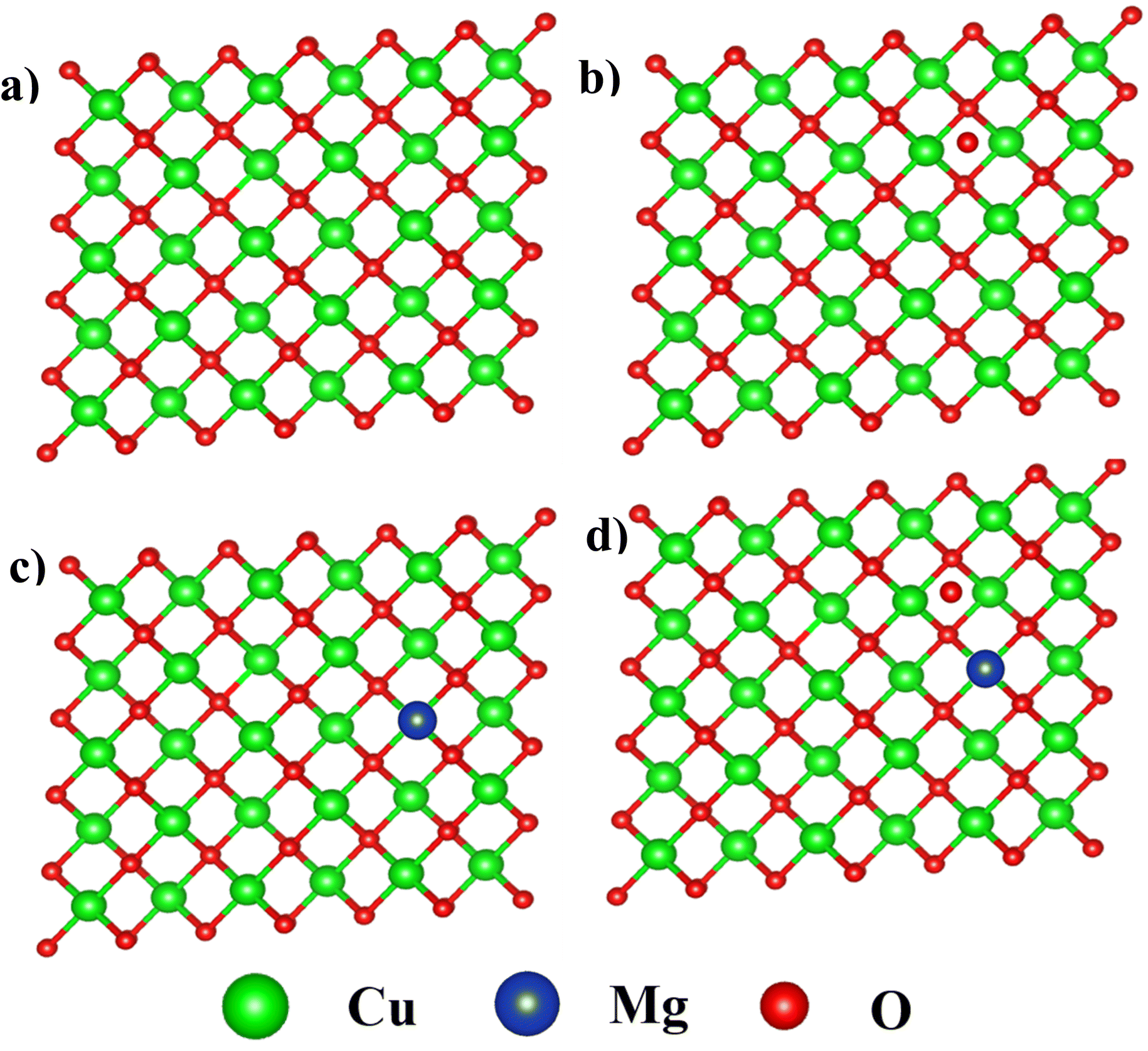 | ||
| Fig. 1 Crystal structure of (a) pure CuO (b) Oi on CuO, (c) Mg doped CuO and (d) Oi on Mg doped CuO. | ||
Results and discussions
Structural characterization
The crystalline structure and phase of CMO samples were identified using XRD. The obtained diffraction pattern is depicted in Fig. 2(a). All the samples exhibited similar diffraction patterns corresponding to the monoclinic phase of CuO thin films. The diffractogram of the films consists of two dominant peaks and a few other minor peaks. The major peaks at 36° and 39° correspond to the reflection from (![[1 with combining macron]](https://www.rsc.org/images/entities/char_0031_0304.gif) 11) and (111) diffraction planes respectively. All the minor peaks were also identified and indexed comparing with the standard JCPDS card (01-077-7718). No other peaks corresponding to other impurity phases like Cu2O or MgO were observed in the diffraction pattern confirming the phase purity of the prepared samples. This indicates that Mg2+ ions can easily penetrate into the CuO lattice without affecting the crystal structure. However, peaks corresponding to (020) and (13) diminished or disappeared from the diffraction pattern with Mg doping which indicates that incorporation of Mg ions has influenced the grain growth in CuO thin films. A higher degree of preferential orientation of CuO planes was therefore observed in doped samples.
11) and (111) diffraction planes respectively. All the minor peaks were also identified and indexed comparing with the standard JCPDS card (01-077-7718). No other peaks corresponding to other impurity phases like Cu2O or MgO were observed in the diffraction pattern confirming the phase purity of the prepared samples. This indicates that Mg2+ ions can easily penetrate into the CuO lattice without affecting the crystal structure. However, peaks corresponding to (020) and (13) diminished or disappeared from the diffraction pattern with Mg doping which indicates that incorporation of Mg ions has influenced the grain growth in CuO thin films. A higher degree of preferential orientation of CuO planes was therefore observed in doped samples.
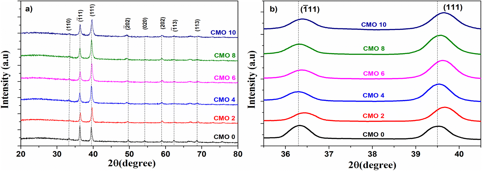 | ||
| Fig. 2 (a) X-ray diffractogram of prepared CMO films, (b) shift in the peak position of (111) and (11) reflection planes. | ||
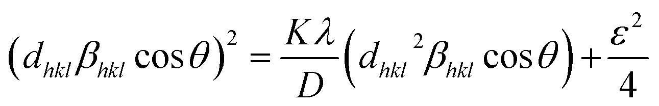
Incorporation of dopant atoms can cause lattice distortions, mainly due to the size difference between the host and dopant atoms. The lattice distortion can be observed from the change in lattice parameters extracted from the XRD data using unit cell software. For monoclinic CuO, lattice parameters a, b, c is related to interfacial angle β and Miller indices h, k, l by,10
 | (1) |
The obtained values of lattice parameters are shown in Table 1. There is an expansion observed along both a and c whereas, the b showed a decrease in its value upon doping. The positions of the two major peaks in the diffractogram are observed to be shifted with Mg doping which is depicted in Fig. 2(b). The position of (111) and (11) showed a shift towards a slightly larger angle. This right shift in the peak position is attributed to the smaller size of Mg2+ ions compared to the Cu2+ ions. When Cu2+ cations are replaced by smaller Mg2+ ions, lattice compression occurs which results in the shift in the peak position towards higher angles.11 A deviation from this trend is shown by (111) peak of CMO 4 and CMO 8 samples in which they show a left shift in the peak position. This can be accounted for by the residual stress developed during the film growth. Residual stress causes anisotropic change in lattice parameters leading to lattice distortion. Tensile stress causes the peaks to shift to lower angles whereas compressive stress shifts the peak towards higher angles.12
| Sample | a (Å) | b (Å) | c (Å) | β (degrees) | V (Å3) |
|---|---|---|---|---|---|
| CMO 0 | 4.574 | 3.370 | 5.070 | 97.78 | 77.45 |
| CMO 2 | 4.598 | 3.353 | 5.082 | 99.39 | 77.29 |
| CMO 4 | 4.625 | 3.333 | 5.095 | 99.48 | 77.47 |
| CMO 6 | 4.621 | 3.319 | 5.092 | 99.56 | 77.02 |
| CMO 8 | 4.624 | 3.325 | 5.103 | 99.57 | 77.36 |
| CMO 10 | 4.630 | 3.315 | 5.097 | 99.69 | 77.11 |
The intensity and full width half maximum (βhkl) of the major peaks in XRD were determined and it was found that the intensity of the peaks decreased, and the peaks broadened after doping. The intensity of diffraction peaks depends on several factors such as the structure factor and atomic scattering factor. When Mg atoms are doped into the CuO lattice, it changes the mean atomic scattering factor and structural factor and there by cause a change in intensity. The broadening of the diffraction peaks is associated with the lattice distortions introduced by the dopant atoms. The orientation of grain growth was determined by calculating the texture coefficient (TChkl)13 given by,
 | (2) |
11) and (111) were calculated and is given in Table 2. It is observed that, before doping, TC11 has a value greater than 1 and after doping it decreased and for doped samples, TC111 is greater than 1. This indicates a clear change in orientation of the crystallites from (11) plane in the undoped film to (111) plane in the doped films.
| Sample | Crystallite size (nm) | Dislocation density (×1016 m−2) | No. of crystallites (×1018 m−2) | TC11 |
TC111 |
|---|---|---|---|---|---|
| CMO 0 | 16 ± 1 | 0.40 | 0.88 | 1.15 | 0.85 |
| CMO 2 | 14 ± 1 | 0.49 | 0.15 | 0.84 | 1.16 |
| CMO 4 | 7 ± 1 | 2.25 | 1.55 | 0.79 | 1.21 |
| CMO 6 | 9 ± 1 | 1.19 | 0.60 | 0.71 | 1.29 |
| CMO 8 | 8 ± 1 | 1.73 | 1.04 | 0.74 | 1.25 |
| CMO 10 | 9 ± 1 | 1.27 | 0.66 | 0.81 | 1.19 |
The size of the crystallites (D) in the films was calculated from size-strain plot15 given by,
 | (3) |
 | (4) |
 | (5) |
Fig. 1 depicts the optimized structure of 3 × 3 × 3 CuO supercell containing 108 atoms of Cu and O each. Optimized k-mesh for the CMO structures were obtained to be 4 × 4 × 4 for kx, ky and kz Brillouin zone as presented in Fig. S1(a).† Structural optimization also been done and the same is depicted in Fig. S1(b).† The minimized energy of these structures signifies the stability of the crystal lattice. To explore the impact of Mg doping, two different concentrations: ∼4 at% and ∼8 at% were theoretically investigated through DFT calculations. Additionally, we computed the formation energy of the CuO crystal structure with intrinsic interstitial oxygen defects. The results revealed a reduction in formation energy from −1.021 eV in pristine CuO to −1.062 eV in 8 at% doped CuO, indicating the stability of CuO post-Mg doping and affirming the suitability of the dopant.
Morphological characterization and elemental analysis
The morphology of the surface of synthesized films were observed using FESEM. Fig. 3 shows the FESEM micrographs of spray deposited pristine and Mg doped CuO thin films. All the films appear to be uniform and crack free with small grains. No pinholes were observed in the FESEM images indicating uniform deposition and good quality of the films. The grain size of the doped films appears to be smaller than that of the pristine samples, indicating that Mg doping has influenced the growth of the grains in the films. The calculated grain size of the films is given in Table 3. The decrease in the grain size of the film upon doping is due to the strain introduced by the dopant atom.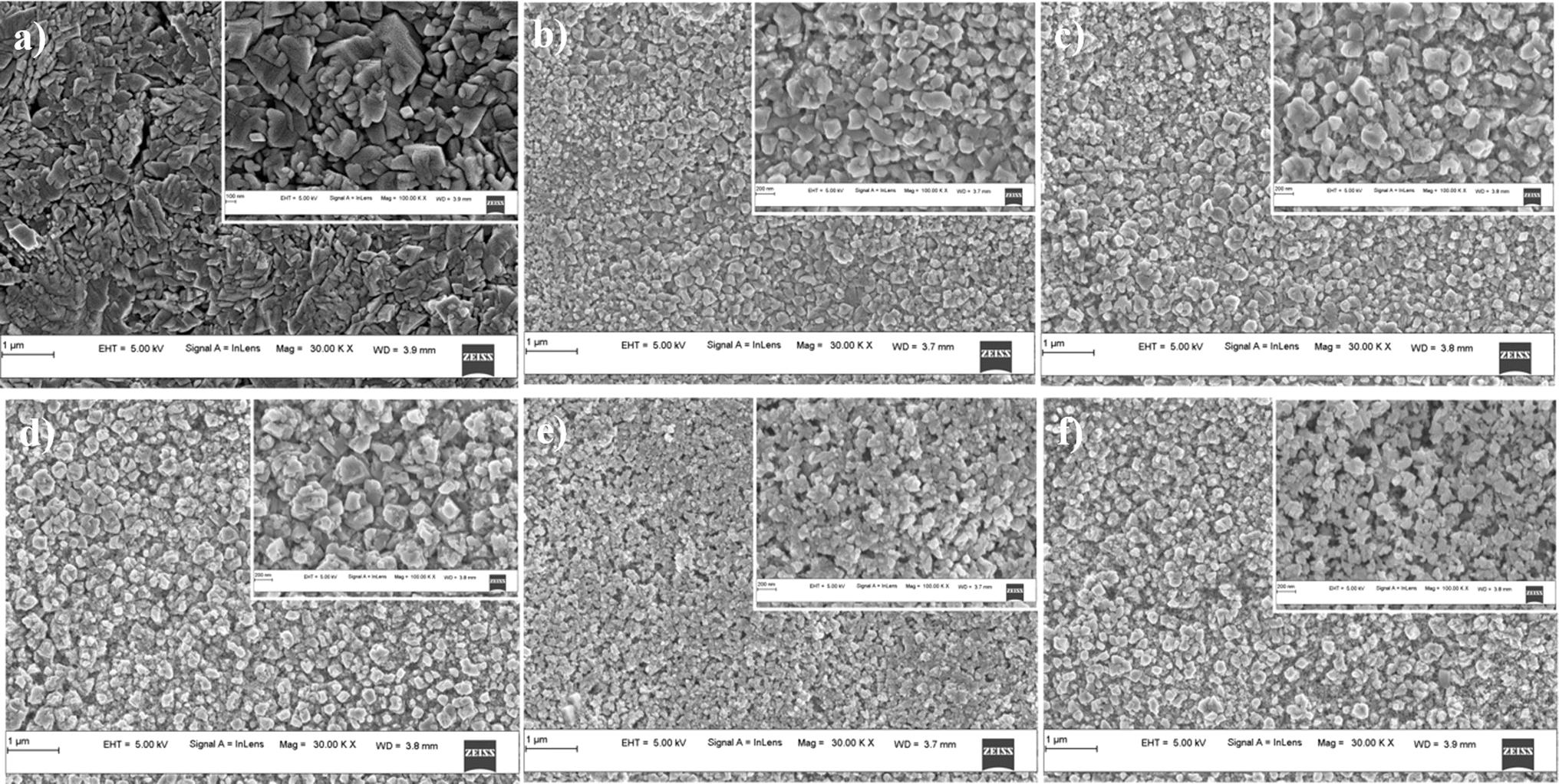 | ||
| Fig. 3 FESEM micrographs (magnification: 30k×) of: (a) CMO 0, (b) CMO 2, (c) CMO 4, (d) CMO 6, (e) CMO 8, (f) CMO 10 thin films (insets show images at 100k× magnification). | ||
| Sample | Cu (at%) | O (at%) | Mg (at%) |
|
Grain size (nm) |
|---|---|---|---|---|---|
| CMO 0 | 46.21 | 53.79 | 0 | 0 | 203 ± 8 |
| CMO 2 | 40.28 | 58.58 | 1.14 | 0.03 (0.04) | 142 ± 4 |
| CMO 4 | 38.94 | 58.79 | 2.28 | 0.06 (0.08) | 106 ± 10 |
| CMO 6 | 38.1 | 58.73 | 3.17 | 0.08 (0.12) | 155 ± 3 |
| CMO 8 | 36.87 | 58.84 | 4.28 | 0.10 (0.16) | 93 ± 4 |
| CMO 10 | 36.10 | 58.84 | 5.06 | 0.12 (0.20) | 102 ± 10 |
The morphology of the Mg doped films appears to be slightly different from that of the undoped film. The doped films have smaller, more or less cubical shaped nanoparticles compared to the large irregularly shaped nanoparticles as observed in the undoped film. This change in the morphology of the films may be associated with the difference in electronegativity of dopant and host atoms. Cu ions have a higher electronegativity value of 1.90 compared to Mg whose electronegativity is 1.31.17 As the electronegativity of Mg is less than Cu, the growth rate of CuO is reduced by Mg doping which causes the morphological variation.11
The composition of elements in the films was studied using EDS. As a representative, the EDS spectrum of CMO 8 is given in Fig. S2(a).† The peaks corresponding to Cu, O and Mg is observed in the spectrum confirming the presence of these elements in the deposited films. The estimated elemental composition of the films is given in Table 3. It is observed that the films have become oxygen rich in nature upon Mg doping. The Mg dopant concentration is found to be less than that of the source values. This deviation may be due to the difference in the reaction mechanism of both Mg and Cu salts.18 The distribution of the elements within the films was obtained using elemental mapping. Fig. S2(b)–(d)† shows the elemental mapping of O, Mg and Cu in CMO 8 sample. The distribution of the elements is observed to be uniform throughout the samples.
UV-Vis spectroscopic analysis
The optical properties of the prepared films were studied using UV-Vis spectroscopy. Fig. 4(a) illustrates the absorption spectra of pristine and Mg doped CuO thin films deposited on glass substrate. All the films exhibited high absorbance in the spectral range of 550–600 nm which makes them suitable for photovoltaic applications. Doping has resulted in an increase in the absorbance of the films, with CMO 10 showing the maximum absorbance at 580 nm. The absorption edge of pristine CuO thin films lies around 748 nm, which showed a nominal shift towards the lower wavelength region indicating a blue shift in the absorbance edge. The blue shift is associated with the smaller crystallite size of the samples after doping.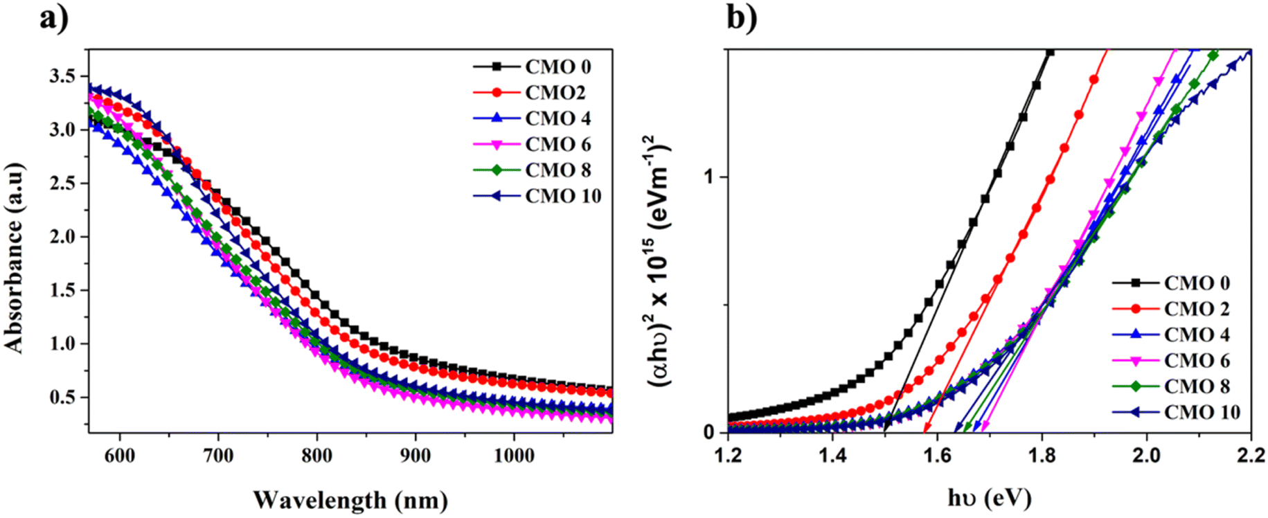 | ||
| Fig. 4 (a) Absorbance spectra and (b) Tauc plot of CMO films. | ||
For direct band gap semiconductors, the optical band gap can be determined from Tauc relation given by,
| αhν = B(hν − Eg)1/2 | (6) |
 | (7) |
We have also simulated the optical spectra using first principle calculations to compare experimental bandgap as well as finding excitonic binding energy for pure and Mg doped CuO (see Fig. S3†). Observed simulated optical absorption spectra are well matched with our experimental findings. Using optical absorption spectra, we have also calculated exitonic binding energy23 and found that in case of Mg doped CuO, exitonic binding energy is higher than pristine samples which is due to doping and interstitial effect in CuO (see Fig. S3†).
Raman analysis
CuO having monoclinic structure belongs to the space group of C2/c (C62h). The primitive unit cell of CuO has two molecules, i.e., four atoms, resulting in three acoustic and nine phonon branches represented as,24| Γ = 4Au + Ag + 5Bu + 2Bg | (8) |
Out of the nine optical modes, six are IR active and three are Raman active modes.25 The Raman modes include the Ag and 2Bg symmetries. The acoustic modes are represented by Au and 2Bu symmetries and the remaining 3Au and 3Bu are IR active modes.26 All the Raman active modes of CuO are because of the displacement of oxygen atoms and in all the cases, Cu atoms remain stationary. This is due to the site symmetry of oxygen atom.27 Ag mode represents the in-phase or out-phase rotation of CuO and Bg1, Bg2 modes are due to the bending of CuO and symmetric stretching of oxygen respectively.28,29
Fig. 5 shows the Raman spectra of Mg doped CuO thin films deposited by spray pyrolysis on glass substrate. Spectra shows all the three Raman active modes which are centred at 293, 342 and 628 cm−1 in the pristine sample. The peak at 293 cm−1 corresponds to the Ag mode whereas the peaks at 342 and 628 cm−1 are assigned to Bg1 and Bg2 modes respectively. These values are in good agreement with those found in the literature.30 While the position of Ag mode remained the same for all the doped samples, there was a shift in the peak positions of Bg modes. This is due to the fact that vibrations of Bg modes are associated with the oxygen atom and the increase in the oxygen content after doping has resulted in the shift in peak position.
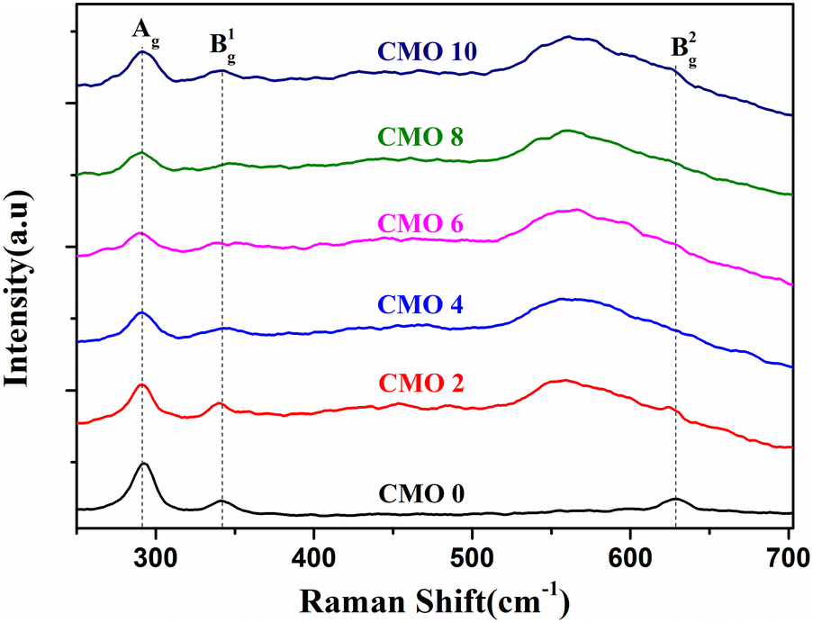 | ||
| Fig. 5 Raman spectra of spray deposited CMO films. | ||
The position of Bg2 mode showed a much higher redshift as compared to Bg1. Also, the Bg2 is much broader compared to other Raman peaks present in the sample. The broadness in Raman peaks is mainly associated with poor crystallinity, the presence of defects and the quantum confinement effect.31 As observed from the XRD, the large redshift and increase in the broadness of the peak can be assigned to a decrease in the crystallite size of the nanoparticles and the confinement of vibrations along the radial direction.31 The broad Raman peaks can also be due to the presence of defects in the system. After Mg-doping, there has been an enhancement in the amount of oxygen present in the sample as observed from EDS. This increase in the oxygen content increased the amount of interstitial oxygen defects, which is detailed in the PL analysis.
Photoluminescence study
The optical properties and defect levels within the band gap of the prepared nanoparticles were studied using photoluminescence (PL) spectroscopy. The deconvoluted PL emission spectra of the synthesized CuO and Mg doped CuO thin films between the wavelength range of 550 to 950 nm is depicted in Fig. 6. All the films showed similar PL spectra with peaks in the green and IR region and a broad emission in the orange-red region. A total of 4 emission bands were observed in the PL spectrum of each sample. The green emission was observed at 565 nm and IR emission at 884 nm. The broad emission at orange–red region were deconvoluted to two peaks centred at 676 and 726 nm.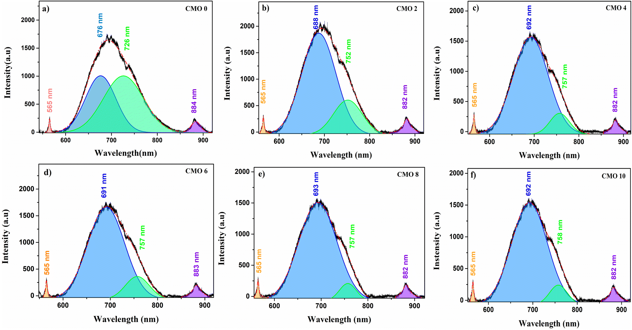 | ||
| Fig. 6 Photoluminescence spectra of (a) CMO 0, (b) CMO 2, (c) CMO 4, (d) CMO 6, (e) CMO 8 and (f) CMO 10 films. | ||
The emissions in PL spectrum can be intrinsic, due to the transition between conduction band and the valence band which are usually referred to as the band edge emission. Along with this there are several defect related emissions known as the extrinsic emission. The peak at 884 nm correspond to the band edge emission. The remaining three peaks are defect related emissions that corresponds to the various defects present in the samples. The intrinsic defects in CuO are mainly due to the Cu vacancies (VCu), Cu interstitials (Cui), oxygen vacancies (Vo) or oxygen interstitials (Oi).32 The peak at 565 nm is from the transition between the exited energy level to the VCu levels.
The red emission at 676 nm is associated with Oi.33,34 As generation of VCu is energetically favoured in the host lattice, a higher concentration of such defects could be expected in CuO nanoparticles. However, VCu being the most stable defect in CuO, doesn't create changes in the electronic structure and doesn't usually contribute to emissions.35 An enrichment of VCu thereby enhances the oxygen ions resulting in Oi defects. Both VCu and Oi act as acceptor levels and enhance the p-type conductivity of CuO.36 The emission at 726 nm corresponds to recombination of electrons from the donor level with the free holes.37 Vo usually acts as the donor level in CuO and hence it can be assumed that this particular emission also corresponds to the oxygen vacancies as well.
The influence of Mg doping in the position and intensity of defect peaks can be observed from Fig. 6. Though the position of both band edge and green emission remained the same, there was an increase in the intensity of these emissions. A significant variation in the intensity and position of defect peaks were observed in the doped samples. While the intensity of both 676 and 726 nm peaks were nearly the same in the case of undoped sample, an enhancement in the intensity of 676 nm peak and a decrease in the intensity of 726 nm peak can be observed with doping. A redshift in the position of these two peaks can also be found. The enhancement in the intensity of 676 nm peak and the redshift of these peaks can be assigned to the increase in the amount of interstitial oxygen defect upon doping.34
To confirm the existence of oxygen at interstitial in Mg doped CuO observed in experimental results, we have done theoretical calculations for the pure and Mg-doped CuO along with O at interstitial positions (see Fig. 7). Formation energies for the pure and Mg-doped CuO along with various kinds of neutral native point defects38 were estimated and observed results have been plotted as functions of the Fermi energy. In the calculations, the zero of the energy was set at the top of the valence band. From the figure, it is clearly observed that interstitial oxygen is the most stable defect with increase in Mg doping as compared to other native defects.
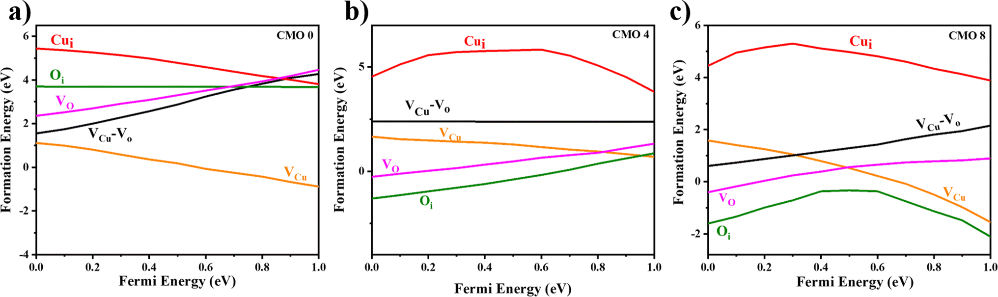 | ||
| Fig. 7 Calculated formation energy of CuO (a) without doping (b) with ∼4 at% Mg doping (c) with ∼8 at% Mg doping. | ||
In isovalent doping, most of the changes in the properties of the films are caused due to lattice deformations introduced by the dopant atom. When dopant atom replaces the metal cations, the surface charge density varies causing a change in the energy of the ionic bond (Ei). Usually, Ei increases as the size of cation decreases. This causes a reduction in the oxygen vacancies.39 The presence of Oi causes an expansion in the CuO lattice which can lead to the redshift observed. This may be the reason for the increase in the a and c lattice parameters as found from XRD. Area ratio of Oi to Vo PL emission peaks were calculated and is given in the Table 4. The Oi/Vo is maximum for CMO 8 indicating that CMO 8 has the maximum Oi defects.
| Sample | E g (eV) | Oi/Vo |
|---|---|---|
| CMO 0 | 1.50 | 0.8 |
| CMO 2 | 1.57 | 3.5 |
| CMO 4 | 1.67 | 8.3 |
| CMO 6 | 1.69 | 6.2 |
| CMO 8 | 1.65 | 12.8 |
| CMO 10 | 1.63 | 10.6 |
X-ray photoelectron spectroscopy
The chemical phase of the prepared film can be further confirmed by identifying the valence state of Cu and other elements present in the sample. The chemical state of the elements present in the film was identified using XPS. The XPS survey spectrum of CMO 8 sample is illustrated in Fig. 8. The survey spectrum included 2p peaks of Cu and Mg along with 1s peaks of O and C. Additional minor peaks corresponding to Cu 3s, 3p and Cu LMM auger peaks were also observed in the spectrum indicating the presence of these elements in the sample. Any shift in the binding energy due to the surface charging is eliminated by carbon correction at 284.8 eV.40 The peaks present in the core spectrum of each element were deconvoluted and fitted using the Gaussian function to separate different species.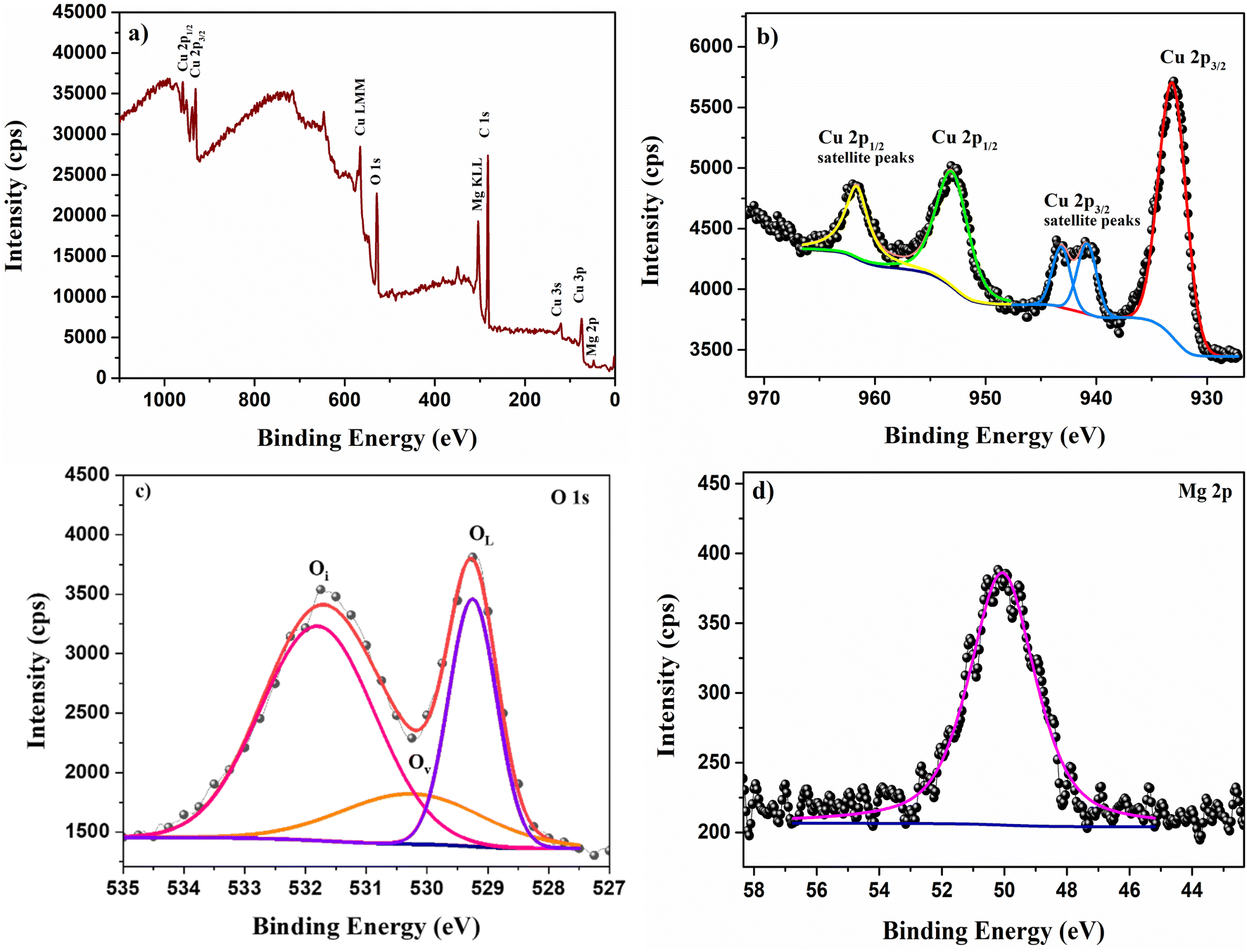 | ||
| Fig. 8 XPS (a) survey and core spectra of (b) Cu 2p, (c) O 1s, (d) Mg 2p subshells. | ||
The fitted profile of the high resolution Cu 2p photoemission spectrum of CMO 8 film (Fig. 8(b)) displayed two prominent peaks centred around 953.02 and 933.12 eV. These two peaks with a peak separation of 19.9 eV is attributed to the spin orbit splitting of 2p orbital state of Cu and is in good agreement with the reported values in the literature.41 The peak at lower binding energy corresponds to Cu 2p3/2 and the one at the higher binding energy represents Cu 2p1/2. Furthermore, strong shake up peaks were observed in the higher binding energy region of both Cu 2p3/2 and Cu 2p1/2. Copper has two stable oxidation states: Cu+ and Cu2+ and the presence of shakeup peaks in the higher binding energy region is a clear indication of +2 oxidation state of Cu.42 Satellite peaks are characteristics of the materials having d9 configuration in the ground state.43 The two shake up peaks at 940.84 and 943.16 eV arise due to the multiplet splitting in 2p5 3d9 configuration.44 These satellite peaks are not observed in the Cu+ configuration as the completely filled d10 configuration does not allow screening via charge transfer to the d states.44 However, Mg doping has resulted in a shift in the peak positions towards lower binding energy. When Mg replaces Cu atoms from the CuO lattice, the difference in the electronegativity creates variation in the electron density cloud of Cu2+. As the electronegativity of Mg is lesser than Cu, the electron density cloud around Cu2+ increases with doping causing a decrease in the binding energy.17
The deconvoluted O 1s core level spectrum is shown in Fig. 8(c). It consists of three peaks located at 529.25, 530.25 and 531.80 eV. The peak at lower binding energy (P1) corresponds to the lattice oxygen and the peak at the middle binding energy (P2) is attributed to the oxygen vacancies.45 The peak at higher binding energy (P3) is associated with interstitial oxygen.45,46 This indicates the co-existence of both Oi and Vo which is also observed in PL spectra. As observed in PL, the area ratio of Oi/Vo is greater than 1 indicating that Oi is the dominant defect in the prepared films which is in line with the PL data. One interesting observation is that the oxygen defect peak corresponding to Oi has a significant area greater than the lattice oxygen itself. Such enhancement in the defect peaks was also observed by M. Nesa et al.47 with Zn doping. Fig. 8(d) displays the fitted profile of Mg 2p containing only a single peak centred at 50.07 eV. This peak is due to the +2 oxidation state of Mg.48 No other peaks corresponding to any other phase were observed in the profile indicating that Mg2+ ions have substituted Cu2+ ions from its lattice, which is backed by both EDS as well as XRD observations.
The percentage composition of the elements present in the sample was quantified from XPS spectra using the relative sensitive factor approach. In this method, we assume that the intensity of the signals corresponding to a given element is proportional to its concentration.49
| Ii = αixi | (9) |
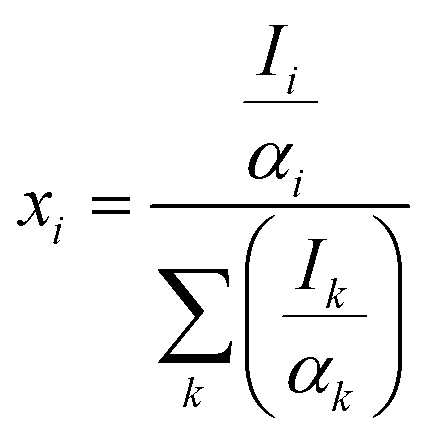 | (10) |
Thus, the calculated amount of Cu, O and Mg present in CMO 8 sample is found to be 36, 60 and 4% respectively. These values are in good agreement with those obtained from EDS results. The higher percentage of O in the samples indicates that our films are oxygen rich in nature.
Electrical properties
The effect of Mg doping on the electrical properties of CuO thin films was studied using Hall measurements. Fig. 9 shows the variation in the obtained electrical properties of doped and undoped films. All the films showed p-type conductivity. The presence of VCu is the primary reason for the p-type conductivity in CuO thin films.50 Mg doping has resulted in a considerable improvement in the conductivity and carrier concentration of CuO films with CMO 8 showing the maximum conductivity and carrier concentration. The carrier concentration of the films was increased by an order of two after doping. The increase in conductivity and carrier concentration can be associated with the defects introduced in the films after doping, especially the oxygen interstitials. Enhancement in the oxygen interstitials increases the p-type conductivity.34–36 The increase in oxygen interstitials with doping is substantiated by the enhanced oxygen content from EDS. Further, the enhanced Oi peaks in PL and the XPS also confirm this observation. Fig. 9(b) represents the variation of carrier density and PL peak area ratio of Oi/Vo with the change in Mg doping concentration. The identical trend in the variation of carrier concentration and Oi/Vo elucidates this argument. On the other hand, the mobility of the films showed an inverse trend. The mobility of the films has declined which is due to the smaller crystallite size. With doping, the carrier concentration has increased, and the grain size has decreased. The change in grain size has influenced the mobility significantly. To see the change in the electronic properties with Mg doping in CuO we have also calculated the total density of states for (a) pure CuO, (b) 4 at% Mg doped CuO and, (c) 8 at% Mg doped CuO (see Fig. S4†). Electronic bandgap of pristine were observed at 1.50 eV and increases to 1.67 eV in case of 4 at% Mg doping while this decreases to 1.65 eV in case of 8 at% Mg doping in CuO. Variation in bandgap is due to structural disorder in case of 8 at% Mg doping and hence it is more favouring Oi and also found in the formation energy calculations.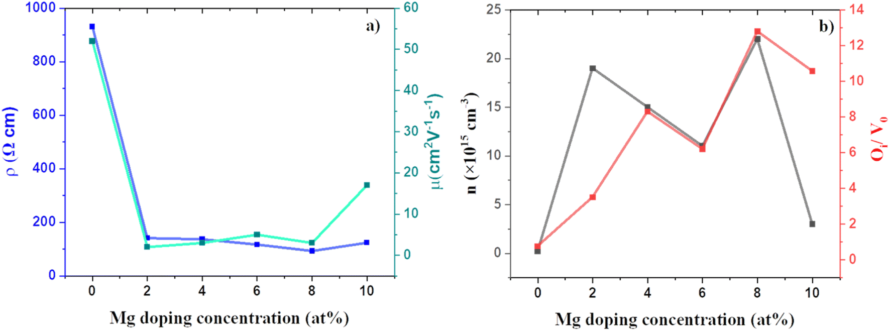 | ||
| Fig. 9 Variation of (a) electrical resistivity, mobility and (b) carrier concentration, area ratio of Oi to Vo PL peaks of CMO films with doping. | ||
Conclusion
The influence of Mg doping on the optoelectronic properties of spray deposited CuO thin films has been investigated. CuO and Mg doped CuO thin film were synthesized over a glass substrate by spray pyrolysis method. Mg doping has resulted in an enrichment of oxygen atoms in the films which has affected structural, optical, and electrical properties. The EDS result revealed the presence of oxygen in excess. The detailed analysis of PL and XPS data has shown that this excess oxygen has remained as interstitials which leads to the lattice expansion. Mg2+ ions, being smaller than Cu2+, were easily incorporated into the CuO lattice without affecting its monoclinic structure. However, the presence of Oi has resulted in the expansion of lattice parameters as observed from XRD results. The crystallite size of the films was observed to be decreased and the band gap of the films widened with doping. Mg doping has improved the conductivity and carrier concentration of the films with CMO 8 showing the least resistivity and maximum carrier concentration. CMO 8 showed the maximum Oi/Vo ratio in PL which explains the maximum conductivity and carrier concentration of this film. Extensive DFT calculations confirms the stability of Oi defects in Mg doped CuO thin films. Presence of Oi in Mg doped CuO shows significant changes in emission and absorption spectra, as well as it also helps to improve the electrical properties. To conclude, Mg doping can be used to improve the electrical properties of CuO films, by enhancing the Oi defects, without compromising their good optical properties and thus can be used for improving the performance of CuO based solar cells.Author contributions
Adithya Prakash: conceptualization, investigation, formal analysis, methodology, visualization, writing – original draft. Vikash Mishra: methodology (DFT calculations). M. G. Mahesha: conceptualization, supervision, writing – review & editing.Conflicts of interest
Authors have no conflict of interest to declare.References
- M. Ajili, S. Dabbabi, N. Bouarissa and N. T. Kamoun, Investigation on substrate effect on physical characteristics of CuO-sprayed thin films suitable for photovoltaic application: Ag/ZnO:Sn (n)/CuO (p)/SnO2:F, Mater. Technol., 2022, 37(6), 381–396, DOI:10.1080/10667857.2020.1854516.
- T. K. S. Wong, S. Zhuk, S. Masudy-Panah and G. K. Dalapati, Current status and future prospects of copper oxide heterojunction solar cells, Materials, 2016, 9(4), 1–21, DOI:10.3390/ma9040271.
- S. Masudy-Panah, K. Radhakrishnan, H. R. Tan, R. Yi, T. I. Wong and G. K. Dalapati, Titanium doped cupric oxide for photovoltaic application, Sol. Energy Mater. Sol. Cells, 2015, 140, 266–274, DOI:10.1016/j.solmat.2015.04.024.
- S. Masudy-Panah, K. Radhakrishnan, A. Kumar, T. I. Wong, R. Yi and G. K. Dalapati, Optical bandgap widening and phase transformation of nitrogen doped cupric oxide, J. Appl. Phys., 2015, 118(22), 225301, DOI:10.1063/1.4936318.
- P. Giannozzi, et al., Advanced capabilities for materials modelling with Quantum ESPRESSO, J. Phys.: Condens. Matter, 2017, 29(46), 465901, DOI:10.1088/1361-648X/aa8f79.
- V. Mishra, et al., Diffuse reflectance spectroscopy: an effective tool to probe the defect states in wide band gap semiconducting materials, Mater. Sci. Semicond. Process., 2018, 86, 151–156, DOI:10.1016/j.mssp.2018.06.025.
- S. Arige, V. Mishra, M. Miryala, M. S. R. Rao and T. Dixit, Plasmon-coupled sub-bandgap photoluminescence enhancement in ultra-wide bandgap CuO through hot-hole transfer, Opt. Mater., 2022, 134, 113149, DOI:10.1016/j.optmat.2022.113149.
- P. Singh, et al., Role of H-bond along with oxygen and zinc vacancies in the enhancement of ferromagnetic behavior of ZnO films: an experimental and first principle-based study, J. Alloys Compd., 2022, 889, 161663, DOI:10.1016/j.jallcom.2021.161663.
- S. Kumar, S. Nandi, V. Mishra, A. Shukla and A. Misra, Anomalous electrochemical capacitance in Mott-insulator titanium sesquioxide, J. Mater. Chem. A, 2022, 10(13), 7314–7325, 10.1039/D1TA10262A.
- N. Thakur, Anu, K. Kumar and A. Kumar, Effect of (Ag, Zn) co-doping on structural, optical and bactericidal properties of CuO nanoparticles synthesized by a microwave-assisted method, Dalton Trans., 2021, 50(18), 6188–6203, 10.1039/d0dt04405a.
- S. U. Din, M. Sajid, M. Imran, J. Iqbal, B. A. Shah, M. Azeem ullah and S. Shah, One step facile synthesis, characterization and antimicrobial properties of Mg-doped CuO nanostructures, Mater. Res. Express, 2019, 6(8), 085022, DOI:10.1088/2053-1591/ab1c1a.
- T. Jiang, Y. Wang, D. Meng and D. Wang, One-step hydrothermal synthesis and enhanced photocatalytic performance of pine-needle-like Zn-doped CuO nanostructures, J. Mater. Sci.: Mater. Electron., 2016, 27(12), 12884–12890, DOI:10.1007/s10854-016-5424-2.
- H. Cavusoglu and R. Aydin, Complexing agent triethanolamine mediated synthesis of nanocrystalline CuO thin films at room temperature via SILAR technique, Superlattices Microstruct., 2019, 128, 37–47, DOI:10.1016/j.spmi.2019.01.011.
- A. Moumen, B. Hartiti and P. Thevenin, Synthesis and characterization of CuO thin films grown by chemical spray pyrolysis, Opt. Quantum Electron., 2017, 49(2), 1–12, DOI:10.1007/s11082-017-0910-1.
- A. Prakash, V. S. Ganesha Krishna, S. N. Moger and M. G. Mahesha, Spectroscopic and electrical analysis of spray deposited copper oxide thin films, Mater. Today Commun., 2022, 32, 103926, DOI:10.1016/j.mtcomm.2022.103926.
- P. Sarker, et al., Effect of gamma irradiation on structural, morphological and optical properties of thermal spray pyrolysis deposited CuO thin film, Ceram. Int., 2021, 47(3), 3626–3633, DOI:10.1016/j.ceramint.2020.09.211.
- Y. Lv, L. Li, P. Yin and T. Lei, Synthesis and evaluation of the structural and antibacterial properties of doped copper oxide, Dalton Trans., 2020, 49(15), 4699–4709, 10.1039/d0dt00201a.
- C. P. Goyal, D. Goyal, S. K. Rajan, N. S. Ramgir, Y. Shimura, M. Navaneethal, Y. Hayakawa, C. Muthamizhchelvan, H. Ikeda and S. Ponnusamy, Effect of Zn doping in CuO octahedral crystals towards structural, optical, and gas sensing properties, Crystals, 2020, 10(3), 188, DOI:10.3390/cryst10030188.
- J. Tauc, R. Grigorovici and A. Vancu, Optical Properties and Electronic Structure of Amorphous Germanium, Phys. Status Solidi B, 1966, 15(2), 627–637, DOI:10.1002/pssb.19660150224.
- S. Ashwani, K. Parveen and D. Sanjay, Structural and Optical Study of Zn doped CuO Nano Particles Synthesized by Sol Gel Method, Int. J. Theor. Appl. Sci., 2017, 9(05), 114–118 Search PubMed.
- R. E. Marotti, P. Giorgi, G. Machado and E. A. Dalchiele, Crystallite size dependence of band gap energy for electrodeposited ZnO grown at different temperatures, Sol. Energy Mater. Sol. Cells, 2006, 90(15), 2356–2361, DOI:10.1016/j.solmat.2006.03.008.
- Y. Wang, T. Jiang, D. Meng, D. Wang and M. Yu, Synthesis and enhanced photocatalytic property of feather-like Cd-doped CuO nanostructures by hydrothermal method, Appl. Surf. Sci., 2015, 355, 191–196, DOI:10.1016/j.apsusc.2015.07.122.
- P. Dey, T. Dixit, V. Mishra, A. Sahoo, C. Vijayan and S. Krishnan, Emergence and Relaxation of an e–h Quantum Liquid Phase in Photoexcited MoS2 Nanoparticles at Room Temperature, Adv. Opt. Mater., 2023, 11(15), 2202567, DOI:10.1002/adom.202202567.
- A. Bhaumik, A. Haque, P. Karnati, M. F. N. Taufique, R. Patel and K. Ghosh, Copper oxide based nanostructures for improved solar cell efficiency, Thin Solid Films, 2014, 572, 126–133, DOI:10.1016/j.tsf.2014.09.056.
- B. K. Meyer, et al., Binary copper oxide semiconductors: from materials towards devices, Phys. Status Solidi B, 2012, 249(8), 1487–1509, DOI:10.1002/pssb.201248128.
- O. Daoudi, A. Elmadani, M. Lharch and M. Fahoume, A new efficient synthesis of CuO thin films using modified SILAR method, Opt. Quantum Electron., 2020, 52(9), 1–17, DOI:10.1007/s11082-020-02530-2.
- P. Chand, A. Gaur, A. Kumar and U. Kumar, Structural and optical study of Li doped CuO thin films on Si (1 0 0) substrate deposited by pulsed laser deposition, Appl. Surf. Sci., 2014, 307, 280–286, DOI:10.1016/j.apsusc.2014.04.027.
- H. Siddiqui and M. R. Parra, Studies of structural, optical, and electrical properties associated with defects in sodium-doped copper oxide (CuO/Na) nanostructures, J. Mater. Sci., 2018, 53(12), 8826–8843, DOI:10.1007/s10853-018-2179-6.
- H. Siddiqui, M. S. Qureshi and F. Z. Haque, Lithium-Doped CuO Nanosheets: Structural Transformation, Optical, and Electrical Characteristics with Enhanced Photocatalytic and Solar Cell Performance, Energy Environ. Mater., 2020, 4(4), 646–657, DOI:10.1002/eem2.12149.
- A. Moumen, et al., Preparation and characterization of nanostructured CuO thin films using spray pyrolysis technique, Superlattices Microstruct., 2019, 127, 2–10, DOI:10.1016/j.spmi.2018.06.061.
- M. F. Saleem, Y. A. Haleem, W. Sun, L. Ma and D. Wang, Surface-enhanced resonance Raman scattering in partially oxidized thin copper film, J. Raman Spectrosc., 2020, 51(8), 1286–1294, DOI:10.1002/jrs.5905.
- A. Živković and N. H. De Leeuw, Exploring the formation of intrinsic p-type and n-type defects in CuO, Phys. Rev. Mater., 2020, 4(7), 1–10, DOI:10.1103/PhysRevMaterials.4.074606.
- F. M. Chang, S. Brahma, J. H. Huang, Z. Z. Wu and K. Y. Lo, Strong correlation between optical properties and mechanism in deficiency of normalized self-assembly ZnO nanorods, Sci. Rep., 2019, 9(1), 1–9, DOI:10.1038/s41598-018-37601-8.
- R. Saha, N. R. Saha, A. Karmakar, G. K. Dalapati and S. Chattopadhyay, Generation of oxygen interstitials with excess in situ Ga doping in chemical bath deposition process for the growth of p-type ZnO nanowires, J. Mater. Sci.: Mater. Electron., 2019, 30, 8796–8804, DOI:10.1007/s10854-019-01204-4.
- B. Troudi, O. Halimi, M. Sebais, B. Boudine and A. Djebli, Synthesis, Structural and Optical Properties of CuO Nanocrystals Embedded in Polyvinyl Chloride (PVC) Thin Films, International Journal of Mechanical and Production Engineering, 2017, 5(2), 115–119 Search PubMed.
- Y. Shen, M. Guo, X. Xia and G. Shao, Role of materials chemistry on the electrical/electronic properties of CuO thin films, Acta Mater., 2015, 85, 122–131, DOI:10.1016/j.actamat.2014.11.018.
- C. Y. Huang, A. Chatterjee, S. B. Liu, S. Y. Wu and C. L. Cheng, Photoluminescence properties of a single tapered CuO nanowire, Appl. Surf. Sci., 2010, 256(11), 3688–3692, DOI:10.1016/j.apsusc.2010.01.007.
- A. Sumanth, V. Mishra, P. Pandey, M. S. R. Rao and T. Dixit, Investigations into the Role of Native Defects on Photovoltaic and Spintronic Properties in Copper Oxide, IEEE Trans. Nanotechnol., 2022, 21, 522–527, DOI:10.1109/TNANO.2022.3204587.
- G. N. Gerasimov, V. F. Gromov, M. I. Ikim and L. I. Trakhtenberg, Effect of Composition and Structure of Metal Oxide Composites Nanostructured on Their Conductive and Sensory Properties, Russ. J. Phys. Chem. B, 2021, 15(6), 1072–1083, DOI:10.1134/S1990793121060038.
- P. Kumar, G. K. Inwati, M. C. Mathpal, S. Ghosh, W. D. Roos and H. C. Swart, Defects induced enhancement of antifungal activities of Zn doped CuO nanostructures, Appl. Surf. Sci., 2021, 560, 150026, DOI:10.1016/j.apsusc.2021.150026.
- O. Lupan, V. Cretu, V. Postica, O. Polonskyi, N. Ababii, F. Schutt, V. Kaidas, F. Faupel and R. Adelung, Non-planar nanoscale p–p heterojunctions formation in ZnxCu1-xOy nanocrystals by mixed phases for enhanced sensors, Sens. Actuators, B, 2016, 230, 832–843, DOI:10.1016/j.snb.2016.02.089.
- M. C. Biesinger, Advanced analysis of copper X-ray photoelectron spectra, Surf. Interface Anal., 2017, 49(13), 1325–1334, DOI:10.1002/sia.6239.
- A. Kaphle, E. Echeverria, D. N. McLlroy and P. Hari, Enhancement in the performance of nanostructured CuO-ZnO solar cells by band alignment, RSC Adv., 2020, 10(13), 7839–7854, 10.1039/c9ra10771a.
- R. Shabu, A. Moses Ezhil Raj, C. Sanjeeviraja and C. Ravidhas, Assessment of CuO thin films for its suitability as window absorbing layer in solar cell fabrications, Mater. Res. Bull., 2015, 68, 1–8, DOI:10.1016/j.materresbull.2015.03.016.
- U. Ilyas, et al., Structural and photoluminescence study of zinc oxide thin films grown by laser induced plasma, in Proceedings of the 5th international conference on the frontiers of plasma physics and technology, 2013, vol. 44, suppl. 37, p. 44083031 Search PubMed.
- H. B. Fan, et al., Investigation of oxygen vacancy and interstitial oxygen defects in ZnO films by photoluminescence and X-ray photoelectron spectroscopy, Chin. Phys. Lett., 2007, 24(7), 2108–2111, DOI:10.1088/0256-307X/24/7/089.
- M. Nesa, M. Sharmin and A. H. Bhuiyan, Role of Zn dopants on the surface morphology, chemical structure and DC electrical transport properties of nanostructured p-type CuO thin films, Mater. Sci. Semicond. Process., 2021, 122, 105479, DOI:10.1016/j.mssp.2020.105479.
- S. Ardizzone, C. L. Bianchi, M. Fadoni and B. Vercelli, Magnesium salts and oxide: an XPS overview, Appl. Surf. Sci., 1997, 119(3–4), 253–259, DOI:10.1016/S0169-4332(97)00180-3.
- A. Jablonski, et al., Quantitative analysis by XPS using the multiline approach, Surf. Interface Anal., 1994, 21(10), 724–730, DOI:10.1002/sia.740211008.
- G. Chaloeipote, R. Prathumwan, K. Subannajui, A. Wisitsoraat and C. Wongchoosuk, 3D printed CuO semiconducting gas sensor for ammonia detection at room temperature, Mater. Sci. Semicond. Process., 2021, 123, 105546, DOI:10.1016/j.mssp.2020.105546.
Footnote |
| † Electronic supplementary information (ESI) available. See DOI: https://doi.org/10.1039/d4ra01414f |
| This journal is © The Royal Society of Chemistry 2024 |