DOI:
10.1039/D4RA01931H
(Paper)
RSC Adv., 2024,
14, 16846-16858
Enhanced solar-driven photoelectrochemical water splitting using nanoflower Au/CuO/GaN hybrid photoanodes
Received
13th March 2024
, Accepted 8th May 2024
First published on 23rd May 2024
Abstract
Harnessing solar energy for large-scale hydrogen fuel (H2) production shows promise in addressing the energy crisis and ecological degradation. This study focuses on the development of GaN-based photoelectrodes for efficient photoelectrochemical (PEC) water splitting, enabling environmentally friendly H2 production. Herein, a novel nanoflower Au/CuO/GaN hybrid structure was successfully synthesized using a combination of methods including successive ionic layer adsorption and reaction (SILAR), RF/DC sputtering, and metal–organic chemical vapour deposition (MOCVD) techniques. Structural, morphological, and optical characteristics and elemental composition of the prepared samples were analyzed using X-ray diffraction (XRD), scanning electron microscopy (SEM), UV-Vis spectroscopy, and energy-dispersive X-ray (EDX) spectroscopy, respectively. PEC and electrochemical impedance measurements were performed for all samples. The nanoflower Au/CuO/GaN hybrid structure exhibited the highest photocurrent density of ∼4 mA cm−2 at 1.5 V vs. RHE in a Na2SO4 electrolyte with recorded moles of H2 of about 3246 μmol h−1 cm−2. By combining these three materials in a unique structure, we achieved improved performance in the conversion of solar energy into chemical energy. The nanoflower structure provides a large surface area and promotes light absorption while the Au, CuO, and GaN components contribute to efficient charge separation and transfer. This study presents a promising strategy for advancing sustainable H2 production via efficient solar-driven water splitting.
1. Introduction
Worldwide energy consumption is quickly expanding and the overall dependence on nonrenewable energy sources is rapidly increasing CO2 levels in the atmosphere, resulting in global warming. Renewable energy sources have attracted the attention of scientists around the world as a solution to this problem.1–3 Hydrogen (H2) exhibits potential to be a dependable substitute energy source owing to its high energy density, environmental friendliness, and ability to be produced from a plentiful supply of water and powerful solar energy.4–6 The photoelectrochemical (PEC) technique for the splitting of water is a promising methodology for the generation of hydrogen from solar light and water using a semiconductor photoelectrode.7,8 The primary challenges with regard to photoelectrode materials, which must be solved for the actual implementation of PEC water splitting include the efficiency and stability of the photoelectrode.9,10 Transition metal oxides,11,12 phosphides,13,14 sulfides,15 hydroxides,16 and carbides17 are commonly employed in the PEC water-splitting process. However, these materials have poor crystal quality, short carrier lifetime, broad band gap and short diffusion length of charge carriers, which all contribute to their poor performance as photoelectrodes in the PEC water-splitting process.18 Metal nitrides have attracted much interest owing to their electrical conductivity and structural stability. Moreover, III–V semiconductors have become promising candidates for the PEC water-splitting process and other applications.19,20 The significant characteristics that make III–V semiconductors suitable candidates for the PEC water-splitting process include crystal quality, band gap tunability, better thermal stability, and prolonged carrier lifetime.21–23 GaN is a III–V semiconductor that exhibits a direct band gap, valence and conduction bands straddling the water redox level (H+/H2 and O2/H2O potentials), a wide emission/absorption spectrum from the infrared to the ultraviolet region. Moreover, it has long-term chemical stability in electrolytes because of the ionic bonds between Ga and N, and it is known to have a high absorption coefficient and excellent transport for charge carriers, all of which boost the PEC activity. Consequently, the GaN photoelectrode is a material that holds the greatest promise for producing H2 via the PEC water-splitting mechanism. GaN has been previously prepared in several ways such as RF magnetron sputtering, pulsed laser deposition, atomic layer deposition, hydride vapour phase epitaxy technique and metal–organic chemical vapour deposition technique.24–29
To achieve more hydrogen generation efficiency via PEC water splitting, a critical issue is the creation of GaN-based materials with enhanced charge transfer and separation efficiency. It has been demonstrated that heterojunctions such as p–n junctions offer a driving force to promote the process of charge separation by the junction's built-in electric field.30 Nevertheless, there has not been much research on the PEC behaviour of heterojunctions made of III-nitride. It is possible to prevent the recombination process of the photo-generated charges and cause extremely effective PEC water-splitting by combining an n-type semiconductor and a p-type semiconductor with a narrow band gap and adequate band potentials for efficient charge separation.31 Accordingly, the fabrication of a junction from GaN and a P-type semiconductor is considered a unique idea for green hydrogen production via the PEC water-splitting process. Copper(II) oxide (CuO) often known as cupric oxide has become one of the most fundamental p-type metal oxide semiconductors in recent years due to its abundance in nature, narrower bandgap, and strong chemical stability. Therefore, it is used in various applications including supercapacitors, solar cells, lithium-ion batteries, photocatalysts, gas sensors, and transistors.32–34 According to the previous discussion, designing a p–n junction from GaN and CuO will contribute greatly to improving the PEC water-splitting efficiency.
This study aims to design a hybrid structure from GaN/CuO decorated with gold (Au) plasmonic metal particles and then investigate its efficiency in PEC cells for H2 production. Combining plasmonic metal particularly gold (Au) with a semiconductor surface is also an effective way to improve the PEC water-splitting process because the creation of a junction between Au plasmonic metal and the photoactive semiconductor aids in the reduction of the recombination rate of electron–hole pairs, it can improve the absorption ability of solar light in the region of visible light due to surface plasmon resonance (SPR) of the Au noble metal, and the SPR makes the charge carriers denser and their transit easier.35,36 Furthermore, during the PEC process, the Au metal can shield the coated semiconductor layer from the photocorrosion process.37 For the composition of the Au/GaN/CuO hybrid structure, different preparation methods were used. Initially, a layer of GaN was well deposited onto a sapphire (Al2O3) substrate via a metal–organic chemical vapour deposition (MOCVD) technique, this process achieved a highly uniform and well-adherent GaN layer. Subsequently, the CuO layer is deposited on GaN via a low-cost successive ionic layer adsorption and reaction (SILAR) technique, and this method has several advantages such as large area deposition, controllable thickness, stoichiometry, morphology, and grain size.38 After that, the GaN/CuO heterostructure was well decorated with Au plasmonic metal by an RF-sputtering common technique for designing Au/GaN/CuO hybrid structures; this procedure enabled the deposition of high-purity samples. Then, the morphological, optical, and chemical characteristics and the PEC water-splitting behaviours were investigated. Numerous performance metrics including current density (Jph) values, conversion efficiencies, and the number of hydrogen moles have also been investigated.
2. Experimental methods
2.1 Materials
All the chemicals were of analytical grade and used without further purification. Copper chloride (CuCl2·2H2O) (Sigma-Aldrich, 98%), ammonium hydroxide (NH4OH) (Sigma-Aldrich, 30%), and water of the highest purity Milli-Q grade (14.9 MΩ cm) were used in the experiment.
2.2 Synthesis of Au/CuO/GaN heterostructures
GaN was grown on a sapphire (Al2O3) substrate via a metal–organic chemical vapour deposition technique. As a purging and carrier gas, nitrogen was utilized. During the procedure, the reactor's pressure was below 10 mbar. After that, using the successive ionic layer adsorption and reaction (SILAR) method, a layer of CuO was deposited onto the GaN layer using a solution containing 0.1 molar copper chloride (CuCl2·2H2O). Ammonia solution was added to the copper chloride solution as a reagent. The CuO layer was successfully grown by alternately dipping the GaN film in the copper chloride-ammonia solution and a hot water solution conserved at 90 °C. The dipping time in every solution was 30 seconds for one cycle, and this process was repeated 20 times for the formation of CuO. It is feasible to summarize the growth of CuO thin films as follows:| | |
CuCl2 + 2NH4OH → Cu(OH)2 + NH4Cl
| (1) |
| | |
Cu(OH)2 + 4NH4OH → [Cu(NH3)4]2+ + 2OH− + 4H2O
| (2) |
| | |
[Cu(NH3)4]2+ + 4H2O → Cu(OH)2 + 4NH4− + 2OH−
| (3) |
Gold (Au) nanoparticles (NPs) were sputtered on CuO/GaN via the DC sputtering technique (LA440S Ardenne). A gold target with high purity (Au, 99.9%) was used to sputter the Au NPs. The sputtering time lasted for 30 seconds; the deposition process was carried out at 0.015 amperes for the DC and 2 torr for the pressure.
2.3 Characterization techniques
XRD was performed using an X-ray diffractometer model (X'pert PRO, Philips, Eindhoven, Netherlands) with monochromatic Cu-Kα operating radiation at 40 kV and 40 mA (0.154056 nm). The analysis was performed at 2θ from 30° to 80° and a temperature of 25 °C to assess the structure and characteristic phase formation. A field emission scanning electron microscope (FESEM, Zeiss sigma 500 VP, Germany) was used to examine the morphological properties of the produced samples. Energy-dispersive X-ray spectrometer equipped with an SEM was also used to analyze the elemental composition and map the elements on the film's surface. The optical characteristics were examined using a UV–Vis spectrophotometer (PerkinElmer Lambda750; Massachusetts, USA) at a wavelength in the range of 350 to 800 nm.
2.4 PEC-measurements
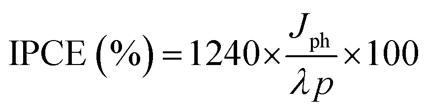
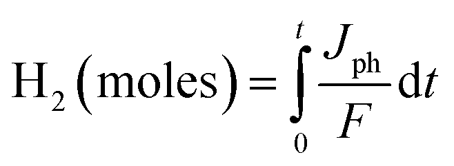
PEC measurements were performed for all produced samples using an Auto-lab Potentiostat with a three-electrode system. The fabricated sample serves as the working electrode; the counter electrode was a platinum sheet, whereas Ag/AgCl acts as the reference electrode. The electrodes were submerged in a solution of Na2SO4 (0.3 M, pH = 7). Linear scan voltammetry was performed between −0.5 V and 1.5 V vs. RHE. A 400 W Xenon lamp was used to illuminate the system to determine the photocurrent density. Numerous computations including the stability, incident photon-to-current conversion efficiency (IPCE%), applied bias photon-to-current efficiency (ABPE%), and electrochemical impedance spectroscopy (EIS) were performed. The evolved hydrogen moles were calculated from the stability experiment (Jph − time) based on the Faraday equation for the Au/CuO/GaN photoelectrode immersed in a 0.3 M Na2SO4 electrolyte under illumination condition and 1.5 V vs. RHE applied voltage.
3. Results and discussion
The XRD patterns of the Au/CuO/GaN heterostructure are displayed in Fig. 1 at a scan rate of about 0.02° s−1, a wavelength of 1.54 Å and 2θ from 30° to 80° As depicted in Fig. 1, the XRD patterns showed the presence of two strong peaks at 35.5° and 38.6° ascribed to the (002) and (111) diffraction planes of the CuO monoclinic phase structure (according to PDF card, no. 01-089-2531). Small and medium intense peaks clearly appeared at 49.8°, 53.3°, 57.1°, 61.6°, and 68.01°, and these peaks also belong to CuO. A small intense peak for metallic gold (Au) presented at 44.4° matches with PDF card, no. 00-066-0091. It is noted that in the Au/CuO/GaN sample, no signals related to the Al2O3 substrate or GaN layer appeared, which can be attributed to the high loaded layer of CuO deposited on the GaN layer. The nano crystallite size (D) of the Au particles was calculated using the Scherrer equation (D = 0.9λ/β![[thin space (1/6-em)]](https://www.rsc.org/images/entities/char_2009.gif) cosθ) with the half width at full maximum (β) of the Au-peak that appeared in the X-ray diffraction pattern of the Au/CuO/GaN sample. The calculated crystallite size of Au particles was approximately 15 nm, whereas β was ∼0.557 radian.
cosθ) with the half width at full maximum (β) of the Au-peak that appeared in the X-ray diffraction pattern of the Au/CuO/GaN sample. The calculated crystallite size of Au particles was approximately 15 nm, whereas β was ∼0.557 radian.
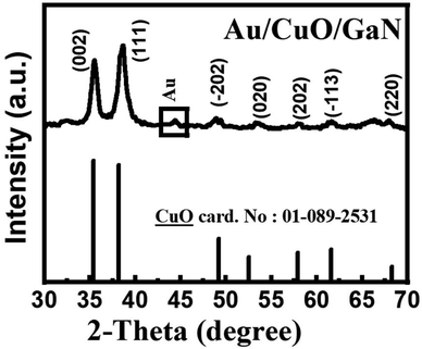 |
| | Fig. 1 XRD diffraction patterns of the Au/CuO/GaN hybrid structure. | |
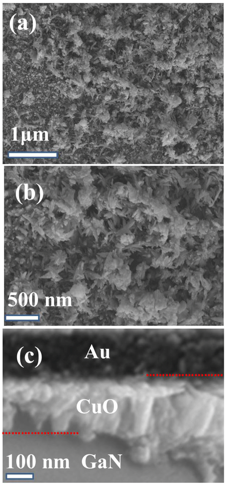
The morphology of the Au/CuO/GaN hybrid structure was examined by scanning electron microscopy (SEM) imaging. Fig. 2a and b shows the high- and low-magnification (1 μm and 500 nm) SEM images. As depicted, the images reveal the presence of flower-like nanostructures (nanoflowers). The flowers are dense and piled on top of each other and appear clearly in the 500 nm magnification image. Fig. 2c depicts the cross-sectional image illustrating the configuration of the Au/CuO/GaN structure. As described in Fig. 2c, three regions appeared at 100 nm scanning representing Au, CuO, and GaN layers. Au appeared on the top surface and looked darker than the under layers.
 |
| | Fig. 2 SEM images of the Au/CuO/GaN hybrid structure: (a) high magnification (1 μm), (b) low magnification (500 nm), and (c) cross section. | |
Nanoflowers are a recently created class of nanoparticles that have a structure resembling a flower. Nanoflowers are made up of several layers of petals that are arranged in a small structure to provide a large surface area for various applications such as drug delivery, biosensing, and catalysis. They exhibited many features including (i) high surface-to-volume ratios that improve the ability of surface adsorption, (ii) better charge transfer, (iii) a three-dimensional structure enhancing the efficiency of surface reactions, and (iv) high surface roughness.39,40 All these features make them distinctive structures for use and accelerate the redox reaction kinetics in the PEC water-splitting process. Nanoflower structures have been reported previously in the literature as effective catalysts for solar energy applications. Ozlem Coskun et al. recorded that the photocurrent density improved to ∼1.3 mA cm−2 for ZnO nanoflower photoanodes in the PEC water-splitting mechanism,41 and Jonathan Harris et al.42 also succeeded in preparing TiO2 nanoflower photocatalysts for the photo-oxidation of methylene blue.
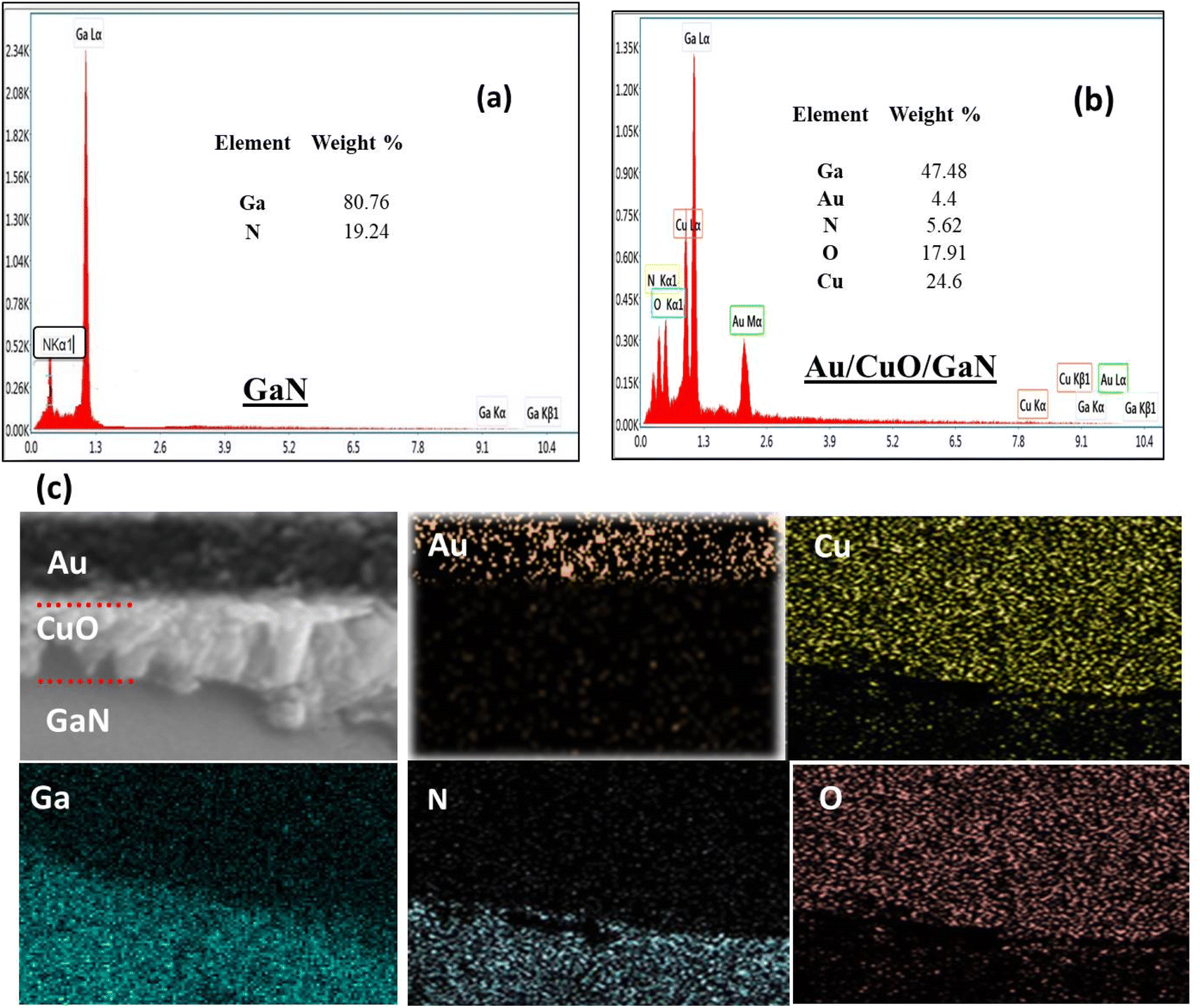
Using an energy-dispersive X-ray spectrometer (EDX), the elemental content of GaN only and the Au/CuO/GaN structure was determined over the cross-sectional area, and elemental mapping was also carried out. The EDX spectra shown in Fig. 3a correspond to GaN and only reveal the presence of N and Ga elements; no peaks were observed for Cu, O and Au. The weight percentage of Ga and N was recorded, and the result is shown in the inset of the figure. Moreover, Cu, O and Au elements appeared in the EDX spectra related to the Au/CuO/GaN structure, as shown in Fig. 3b. It is noted that in the GaN region, the weight percentages of Ga and N are relatively high compared to the Au/CuO/GaN structure. The elemental mapping of the elements that appeared in the full cross-sectional area is displayed in Fig. 3c.
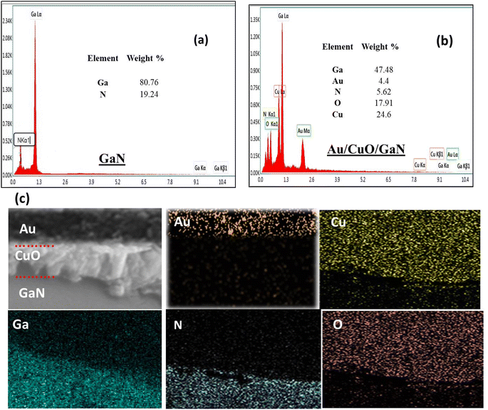 |
| | Fig. 3 (a) EDX spectra of the GaN region, (b) EDX spectra of the Au/CuO/GaN hybrid structure photoelectrodes, and (c) mapping of the Au/CuO/GaN hybrid structure photoelectrode. | |
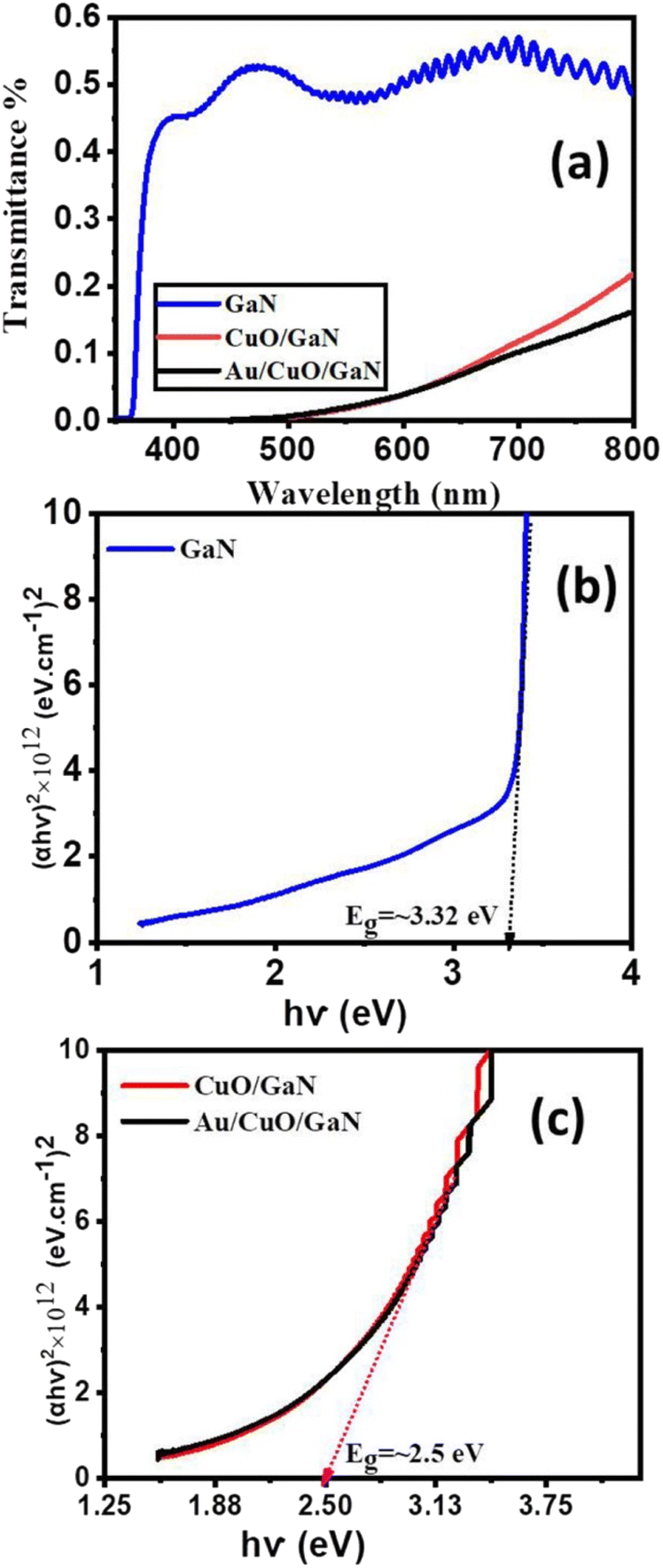
The transmittance spectra of the prepared samples were analyzed using a UV-visible spectrophotometer. The wavelengths ranged from 350 nm to 800 nm (encompassing the visible, ultraviolet, and near-IR spectrums). As shown in Fig. 4a, the produced samples exhibited a maximum transmittance value ranging from 0.1% to 0.5% suggesting that samples with high absorption values were generated. The maximum transmittance value (0.5%) was found in GaN samples; this value declined upon deposition of the CuO layer, and the metallic Au above the GaN layer and attained the lowermost value (0.1%) for the Au/CuO/GaN sample. For the GaN sample from 350 nm to 362 nm, the transmittance value is close to zero after that, and the value starts to increase. Moreover, for CuO/GaN and Au/CuO/GaN samples, the transmittance is comparable to zero from 350 nm to 500 nm, which is an indication of the widening of the absorption limit after the deposition of CuO and metallic Au over GaN. For more investigation, the energy gap (Eg) was measured for all samples in Fig. 4b and c using the Tauc relation (αhν)2 = B(hν − Eg). The measured Eg value for CuO/GaN and Au/CuO/GaN structures was almost the same (∼2.5 eV), and for GaN, only Eg was higher than that of the hybrid structures (∼3.32 eV).
 |
| | Fig. 4 (a) Transmittance spectra of the prepared samples. (b and c) Tauc plot of all samples. | |
The photoelectrochemical behavior of the prepared samples was evaluated using a three-electrode PEC cell system and simulated solar irradiation (AM 1.5G). The three electrodes included the working electrode, which represented the fabricated sample, the counter electrode (Pt-sheet) and the reference electrode (Ag/AgCl). Fig. 5a shows the Jph–V curves of GaN, CuO/GaN and Au/CuO/GaN photoanodes in the 0.1 M Na2SO4 electrolyte, and the scan rate was 10 mV s−1. In the absence of light (dark condition), the Jph–V curves were insignificant, and under the illumination condition, the photocurrent density (Jph) of the prepared samples increased with the increase in the applied bias. The highest value of Jph at 1.5 V vs. RHE in the case of GaN reached ∼0.8 mA cm−2, while in the case of CuO/GaN and Au/CuO/GaN samples, the highest value of Jph was comparable to 2 mA cm−2 and 4 mA cm−2 respectively. It is noted that by depositing a CuO layer on GaN, the maximum Jph value increased from 0.8 to 2 mA cm−2, because CuO/GaN exhibited a type-II band alignment which achieved effective separation of the photogenerated charge carriers, thereby enhancing the PEC performance.43
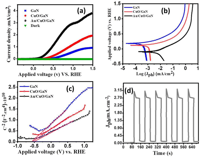 |
| | Fig. 5 (a) Jph–V curves of all samples in a 0.1 M Na2SO4 electrolyte. (b) Tafel plots of all samples. (c) Mott–Schottky measurements for all samples. (d) Transient photocurrent measurement of the Au/CuO/GaN hybrid structure. | |
The Tafel plot characteristics were assessed to determine the mechanism underlying the HER process, the Tafel plots for all samples are displayed in Fig. 5b. The Tafel slopes were calculated using the relation V = βlog(Jph) + c. The anodic (βa) and cathodic (βc) Tafel slopes are depicted in Table 2. Compared with the GaN electrode, the Au/CuO/GaN hybrid structure exhibited the smallest value of βa and βc slopes. A low Tafel slope value for the hybrid structure implies the high hydrogen evolution efficiency. For more investigation, the Mott–Schottky analysis (MS) was performed for all samples for the investigation of the carrier concentrations in addition to the confirmation of the photoanode behaviours of the samples. The resulting Mott–Schottky plots with the corresponding linear fitting were depicted in Fig. 5c. The positive slopes for all samples confirmed their photoanode behaviours. The concentration of the charge carriers (ND) was calculated using the obtained slopes via the relation ND = (2/eεε0) × (slope)−1. The obtained concentrations were ∼5 × 1018 cm−3, ∼9 × 1018 cm−3 and ∼13 × 1018 cm−3 for GaN, CuO/GaN and Au/CuO/GaN, respectively. The high carrier concentration for the Au/CuO/GaN anode may have resulted from the deposition of the plasmonic gold layer. Fig. 5d displays the transient current behaviour of the Au/CuO/GaN hybrid structure under white light illumination at 1.5 V vs. RHE in a 0.3 M Na2SO4 electrolyte, and Jph was found to be stable and high, which displayed reliable on/off photocurrent characteristics.
In the PEC experiment, a voltage was carried out between the counter and working electrodes to examine the PEC characteristics including stability, Jph–V curve, and electrochemical impedance. This applied voltage played an effective role in the acceleration of the transportation process for charge carriers between the working and counter electrodes, which would affect the PEC's activity. As a result, the applied biased photon-to-current conversion efficiency (ABPE%) was used to subtract the excessive voltage, as described in eqn (5):44,45
| |
 | (5) |
where
Jph stands for the photocurrent density,
V bias is the applied voltage, and
P refers to the incoming light intensity (100 mW cm
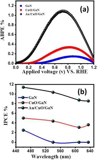
−2). ABPE% for all photoanodes under white light illumination is shown in
Fig. 6a. It is noted that the Au/CuO/GaN sample exhibited a value of 0.015% for the ABPE% at 0 V
vs. RHE, revealing a good rate of light utilization compared to other samples.
 |
| | Fig. 6 (a) ABPE% for all photoanodes under white light illumination. (b) Different values of IPCE% as a function of wavelength for all samples. | |
The photo-generated charge carriers collected for each incident photon at a certain wavelength are expressed as the external quantum efficiency (EQE) or incident photon-to-current conversion efficiency (IPCE%). Eqn (6) was used to estimate the IPCE% for all prepared samples at 1.5 V vs. RHE:46
| |
 | (6) |
where
p is the illuminating power (100 mW cm
−2) and
λ is the incoming photons' wavelength in nanometers. The IPEC efficiency was calculated at wavelengths ranging from 460 to 636 nm; for all samples, the maximum value was recorded at 460 nm. Different values of IPCE% as a function of wavelengths for all samples are displayed in
Fig. 6b. GaN-based photoelectrodes exhibited a maximum value for IPCE equal to ∼2.6%, while in the case of CuO/GaN, the value was ∼5%. The calculated IPCE% for Au/CuO/GaN was ∼11.5% at 460 nm. As discussed, the Au/CuO/GaN sample exhibited the highest efficiency and photocurrent density; this can be attributed to the role of the plasmonic gold metal that decorated the sample. The function of plasmonic Au in the PEC process has several interpretations including following, (i) photoabsorption can be improved as a result of increased photons scattering by loaded Au nanoparticles on the surface of the CuO/GaN heterostructure but this explanation takes place only if Au particles greater than 50 nm;
47 (ii) the interaction between the localized electric field of Au metal and the semiconductor can also lead to an increase in the interband transition within it and hence improve the PEC activity,
48,49 to clarify more the Au metal can support a localized surface plasmon included the visible light region resulted in a radiated energy, this energy included the visible region and can be transported to the semiconductor resulting in creation electron–hole pairs within it and this depended on the energy gap of the semiconductor, the band gap needed to be within the visible region energy in order to enhance the PEC efficiency for this semiconductor. Herein, this radiative energy which includes the visible light region is insufficient to create a pair of electrons and holes as the energy gap of CuO is comparable to ∼1.2 eV; therefore, this effect can also be excluded in improving the efficiency;
50 (iii) a hot electron will be injected from Au towards the conduction band of the CuO layer by the action of the surface plasmon resonance (SPR), and thus, the number of conduction band electrons in CuO is increased with the aid of Au plasmonic metal. Here, this effect is likely to have the highest impact on increasing the PEC activity. It is important to note that CuO/GaN displayed a type II junction, meaning that the level of the CuO conduction band is higher than that of GaN. As a result, electrons from the CuO conduction band can be injected into the GaN conduction band based on their band alignment, effectively separating the photogenerated charge carriers and increasing PEC efficiency.
43,49
We will therefore focus on and conclude the other PEC investigations using Au/CuO/GaN as the ideal photoanode among other samples, as it showed the highest efficiency and photocurrent density. As shown in Fig. 7a, the stability of the Au/CuO/GaN heterostructure was investigated under white light illumination at 1.5 V vs. RHE in a 0.3 M Na2SO4 electrolyte. The photocurrent density was lowered from its beginning value (∼3.75 mA cm−2) to roughly 2.9 mA cm−2 after ∼65 s, and then, the value of Jph stabilized at 3.06 mA cm−2. The reason for this sudden drop in the Jph value is the photo corrosion process that takes place between the photoelectrode and the electrolyte. Theoretically, Faraday's rule in eqn (7) was used to determine the moles of hydrogen produced by the PEC water splitting process:51
| |
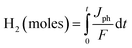 | (7) |
where
F denotes the Faraday constant (9.65104 C mol
−1) and
t represents the time. The produced moles of hydrogen as a function of time are presented in
Fig. 7b, which was estimated using the measured
Jph − time data. The number of hydrogen moles was 3246 μmol h
−1 cm
−2. In comparison to the previously validated GaN-based PEC photoelectrodes, the optimized Au/CuO/GaN photoelectrode in this work demonstrated a greater photocurrent density and conversion efficiency.
Table 1 presents an overview of our Au/CuO/GaN electrode's PEC performances in comparison to other GaN-based photoelectrodes found in the literature.
 |
| | Fig. 7 (a) Stability of the Au/CuO/GaN heterostructure under white light illumination at 1.5 V vs. RHE in a 0.3 M Na2SO4 electrolyte. (b) Produced moles of hydrogen as a function of time. | |
Table 1 Previous studies of GaN-based electrodes for the PEC water-splitting process
| Sample |
Photocurrent density (mA cm−2) |
Voltage vs. RHE (V) |
Electrolyte |
Light intensity (mW cm−2) |
Ref. |
| InGaN/GaN |
0.16 |
2 |
0.1 M Na2SO4 |
100 |
63 |
| ZnS/AuNPs/GaN |
1.15 |
0 |
1 M NaOH |
100 |
2 |
| GaN NRs/Ta foil |
0.165 |
0.6 |
1 M oxalic acid |
100 |
64 |
| NiO/GaN |
0.4 |
0.5 |
1 M HCl |
100 |
65 |
| GaN NRs |
0.3 |
0 |
1 M NaOH |
90 |
66 |
| p–n GaN |
0.16 |
1.23 |
0.1 M Na2SO4 |
100 |
67 |
| GaN nanowire/Si |
0.55 |
0 |
1 M NaOH |
100 |
68 |
| InGaN |
2.4 |
1.6 |
1 M HBr |
100 |
69 |
| n-GaN |
0.15 |
0.8 |
1 M NaOH |
100 |
70 |
| Au/CuO/GaN |
4 |
1.5 |
0.3 M Na2SO4 |
100 |
This work |
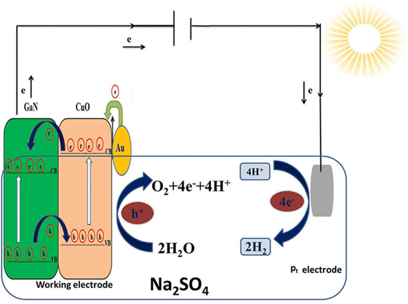
Comprehending the formation, separation and movement of the photoexcited electron–hole pairs within the Au/CuO/GaN heterostructure system is crucial in clarifying its improved PEC water-splitting capabilities. The suggested mechanism for the charge transfer process through the Au/CuO/GaN hybrid structure is displayed in Fig. 8. CuO has a work function of around 5.97 eV, which is larger than the work function of Au (5.1 eV), revealing that the CuO layer has a substantially lower Fermi level than Au.52,53 As a result of the decoration of CuO/GaN with Au, the electrons will successfully drift from Au to CuO because of the obvious differences in Fermi levels until the balanced state is achieved for the Fermi levels in both materials; therefore, a Schottky barrier is established between Au and CuO, leading to a downward band bending for CuO. Under the illumination conditions, the hot energetic electrons created in the Au layer will successfully overcome the Schottky barrier and be injected into the conduction band of CuO, which causes the formation of holes in Au and the accumulation of the hot electron in the conduction band of CuO. Moreover, the incident photons on the CuO layer will make a photoexcitation process and create photogenerated electrons and holes inside it. Based on the CuO/GaN heterostructure's band alignment, both the electrons generated by the incident light and the hot energetic electrons injected by Au in the CuO conduction band will further transfer from the conduction band of CuO to the conduction band of GaN. Then the injected and generated electrons in the conduction band of GaN will transfer to the external circuit and arrive at the platinum electrode for achieving the reduction process of H+ to H2 on this electrode. Furthermore, the photo-generated holes created near the surface of CuO and Au layers will be responsible for achieving the oxidation process of water to O2 via the capture of electrons from the electrolyte (water) and form O2.54
 |
| | Fig. 8 Suggested mechanism of the charge transfer process through the Au/CuO/GaN hybrid structure. | |
In order to examine the charge transfer processes taking place at the interface between the semiconductor and the electrolyte, electrochemical impedance spectroscopy (EIS) was applied to the prepared photoanodes. The experiment was tested at 0 V vs. RHE, room temperature (∼25 °C) and frequencies between 0.01 Hz and 100 kHz. Additionally, the ZsimpWin software was employed for fitting the obtained data and the extraction of the equivalent circuit. Fig. 9 displays the Nyquist plots of the fitted and experimental EIS data for all photoelectrodes; the experimental data are indicated by symbols, and the fitting curves are displayed as dashed lines. The circuit model used to fit the obtained EIS data is provided in the insets of Fig. 9a; it is simply composed of three elements, namely, Rs, Rct and CPE. The values of the equivalent circuit parameters are recorded in Table 2. Rs is the electrolyte resistance which represents the resistance of the charges within the electrolyte. For the GaN sample Rs was recorded as 97.95 Ω cm2, and this value diminished to 15.14 Ω cm2 for the Au/CuO/GaN hybrid structure. Rct denotes the resistance for the movement of the charges across the interface between the photoanode and the electrolyte, and the more effective charge transport could be provided by the small value of Rct. Rct is signified by the diameter of the semicircle in the Nyquist plot, where it decreases as the semi-circle size decreases.55,56 Rct exhibited the highest value for GaN as 49902 Ω cm−2, and this value decreased to 3748.8 Ω cm−2 and 102.79 Ω cm−2 for CuO/GaN and Au/CuO/GaN, respectively. The low Rct value for Au/CuO/GaN compared with the other samples justifies the large obtained photocurrent density. The capacitance corresponding to the double layer formed between the active electrode and the electrolyte can be indicated by the constant phase element (CPE).57–59 Generally, CPE may manifest as a result of (i) the nature of the electrode, (ii) porosity, and (iii) the inhomogeneity of the electrode–electrolyte interface.60,61 CPE is described in eqn (8):62
| |
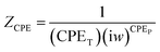 | (8) |
where CPE
T and CPE
P are constants that are independent of frequency and
w represents the angular frequency. The constant phase element is identified by two values of CPE
T and CPE
P. The value of CPE
T is associated with the capacitance and active area, whereas CPE
P is the exponent of the constant phase element and it corresponds to the surface roughness of the photoelectrode; rougher surfaces correlate with lower CPE
P values. The CPE
P values range from 0 to 1, and for ideal capacitance without defects, CPE
P is 1, whilst CPE
P values of 0 and 0.5 signify a resistance and Warburg behavior, respectively.
60 As presented in
Table 2, Au/CuO/GaN recorded the highest value for CPE
T (2.5 × 10
−6 F cm
−2), which implies that it acquired a large capacitance among the other electrodes; moreover, a lower value of CPE
P (0.83) indicates its high roughness value. Finally, from the impedance data, it was observed that the Au/CuO/GaN hybrid structure achieved a lower value for
Rs,
Rct and CPE
P and a larger value for CPE
T. All these factors made it an influential electrode in the PEC water-splitting process compared with the other electrodes.
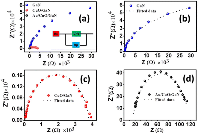 |
| | Fig. 9 Nyquist plots of the fitted and experimental EIS data of (a) the three photoelectrodes, (b) GaN photoelectrode, (c) CuO/GaN photoelectrode, and (d) Au/CuO/GaN photoelectrode. | |
Table 2 Values of the equivalent circuit parameters obtained from EIS data and anodic (βa) and cathodic (βc) Tafel slopes
| Sample |
Rs (Ω cm−2) |
Rct (Ω cm−2) |
CPET (F cm−2) |
CPEP (—) |
βa (mV dec−1) |
βc (mV dec−1) |
| GaN |
97.95 |
49902 |
6.7 × 10⁻⁸ |
0.97 |
225 |
780 |
| CuO/GaN |
54.85 |
3748.8 |
1.1 × 10⁻⁷ |
0.91 |
173 |
1055 |
| Au/CuO/GaN |
15.14 |
102.79 |
2.5 × 10⁻⁶ |
0.83 |
170 |
590 |
For the investigation of the purity of the Au/CuO/GaN photoanode, XRD diffraction patterns were performed after PEC tests. Fig. 10 displays the comparison between the peaks before and after PEC measurements. After the PEC measurements, there was no change in the peak positions or the emergence of new ones, indicating its high stability. However, the intensity of the peaks slightly decreased compared with the previous PEC tests. This implied the good stable nature of the Au/CuO/GaN photoanode.
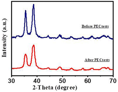 |
| | Fig. 10 XRD diffraction patterns before and after the PEC test for the Au/CuO/GaN photoelectrode. | |
4. Conclusion
In summary, high-quality nanoflower Au/CuO/GaN hybrid structures have been successfully prepared by a combination of techniques, namely, successive ionic layer adsorption and reaction (SILAR), RF/DC sputtering, and metal–organic chemical vapour deposition (MOCVD). X-ray diffraction (XRD) analysis revealed the presence of sharp and strong peaks at 35.5° and 38.6°, ascribed to the (002) and (111) lattice planes, respectively, indicating the monoclinic phase of CuO according to the reference (PDF card, no. 01-089-2531). A small intense peak at 44.4° confirmed the presence of metallic gold. Scanning electron microscopic (SEM) images displayed the nanoflower morphology at both high (1 μm) and low magnifications (500 nm). Energy-dispersive X-ray (EDX) spectra confirmed the presence of N, Ga, Cu, O and Au elements in the hybrid structure. Transmittance spectra showed low values, indicating enhanced absorption of the samples within the 350 nm to 800 nm range. Photoelectrochemical (PEC) measurements revealed an incident photon-to-current conversion efficiency (IPCE%) of approximately 11.5% at 460 nm, while the anodic photocurrent bias potential efficiency (APBE%) was recorded as 0.015% at 0 V vs. RHE. Electrochemical impedance spectroscopy (EIS) measurements exhibited low values for a series resistance (Rs) of 15.14 Ω cm−2 and a charge transfer resistance (Rct) of 102.79 Ω cm−2, indicating the highly effective performance of the nanoflower Au/CuO/GaN hybrid structures in the PEC water-splitting process. This study demonstrates the efficient preparation and characterization of high-quality nanoflower Au/CuO/GaN hybrid structures, highlighting their potential for enhanced photoelectrochemical water-splitting applications.
Data availability
All data are available within the manuscript.
Conflicts of interest
There are no conflicts to declare.
Acknowledgements
The authors extend their sincere appreciation to the Researchers Supporting Project number (RSP2024R55), King Saud University, Riyadh, Saudi Arabia for the funding support.
References
- T. Ahmad and D. Zhang, A critical review of comparative global historical energy consumption and future demand: The story told so far, Energy Rep., 2020, 6, 1973–1991 CrossRef.
- A. Abdullah, I. V. Bagal, A. Waseem, M. A. Kulkarni, H. Thaalbi and J. K. Lee, et al., Engineering GaN nanowire photoanode interfaces for efficient and stable photoelectrochemical water splitting, Mater. Today Phys., 2022, 28, 100846 CrossRef CAS.
- Z. Wang, J. Fan, B. Cheng, J. Yu and J. Xu, Nickel-based cocatalysts for photocatalysis: Hydrogen evolution, overall water splitting and CO2 reduction, Mater. Today Phys., 2020, 15, 100279 CrossRef.
- C. Koroneos, A. Dompros, G. Roumbas and N. Moussiopoulos, Advantages of the use of hydrogen fuel as compared to kerosene, Resour., Conserv. Recycl., 2005, 44, 99–113 CrossRef.
- I. Staffell, D. Scamman, A. Velazquez Abad, P. Balcombe, P. E. Dodds and P. Ekins, et al., The role of hydrogen and fuel cells in the global energy system, Energy Environ. Sci., 2019, 12, 463–491 RSC.
- X. Yang, W. Liu, C. Han, C. Zhao, H. Tang and Q. Liu, et al., Mechanistic insights into charge carrier dynamics in MoSe2/CdS heterojunctions for boosted photocatalytic hydrogen evolution, Mater. Today Phys., 2020, 15, 100261 CrossRef.
- W. Yang, R. R. Prabhakar, J. Tan, S. D. Tilley and J. Moon, Strategies for enhancing the photocurrent, photovoltage, and stability of photoelectrodes for photoelectrochemical water splitting, Chem. Soc. Rev., 2019, 48, 4979–5015 RSC.
- M. A. Marwat, M. Humayun, M. W. Afridi, H. Zhang, M. R. Abdul Karim and M. Ashtar, et al., Advanced catalysts for photoelectrochemical water splitting, ACS Appl. Energy Mater., 2021, 4, 12007–12031 CrossRef CAS.
- Y.-H. Chiu, T.-H. Lai, M.-Y. Kuo, P.-Y. Hsieh and Y.-J. Hsu, Photoelectrochemical cells for solar hydrogen production: Challenges and opportunities, APL Mater., 2019, 7, 080901 CrossRef.
- A. Thakur, D. Ghosh, P. Devi, K.-H. Kim and P. Kumar, Current progress and challenges in photoelectrode materials for the production of hydrogen, Chem. Eng. J., 2020, 397, 125415 CrossRef CAS.
- N. Hassan, A. Jalil, N. Khusnun, A. Ahmad, T. Abdullah and R. Kasmani, et al., Photoelectrochemical water splitting using post-transition metal oxides for hydrogen production: a review, Environ. Chem. Lett., 2022, 1–23 Search PubMed.
- P. Pattanayak, P. Singh, N. K. Bansal, M. Paul, H. Dixit and S. Porwal, et al., Recent progress in perovskite transition metal oxide-based photocatalyst and photoelectrode materials for solar-driven water splitting, J. Environ. Chem. Eng., 2022, 108429 CrossRef CAS.
- Y. Wang, B. Kong, D. Zhao, H. Wang and C. Selomulya, Strategies for developing transition metal phosphides as heterogeneous electrocatalysts for water splitting, Nano Today, 2017, 15, 26–55 CrossRef CAS.
- Y. Li, Z. Li, C. Xu, S. Yu and Z. Sun, Facile preparation of nickel phosphide for enhancing the photoelectrochemical water splitting performance of BiVO4 photoanodes, RSC Adv., 2023, 13, 8374–8382 RSC.
- H. Wang, Y. Xia, H. Li, X. Wang, Y. Yu and X. Jiao, et al., Highly active deficient ternary sulfide photoanode for photoelectrochemical water splitting, Nat. Commun., 2020, 11, 3078 CrossRef CAS PubMed.
- X. Ning, P. Du, Z. Han, J. Chen and X. Lu, Insight into the Transition-Metal Hydroxide Cover Layer for Enhancing Photoelectrochemical Water Oxidation, Angew. Chem., Int. Ed., 2021, 60, 3504–3509 CrossRef CAS PubMed.
- X. Han, S. Heuser, X. Tong, N. Yang, X. Y. Guo and X. Jiang, Epitaxial Cubic Silicon Carbide Photocathodes for Visible-Light-Driven Water Splitting, Chem.–Eur. J., 2020, 26, 3586–3590 CrossRef CAS PubMed.
- D. Li, J. Shi and C. Li, Transition-Metal-Based Electrocatalysts as Cocatalysts for Photoelectrochemical Water Splitting: A Mini Review, Small, 2018, 14, 1704179 CrossRef PubMed.
- W. Z. Tawfik, S.-J. Bae, S. B. Yang, T. Jeong and J. K. Lee, Stress Engineering by Controlling Sapphire Substrate Thickness in 520 nm GaN-Based Light-Emitting Diodes, Appl. Phys. Express, 2013, 6, 122103 CrossRef.
- W. Z. Tawfik, M. A. Hassan, M. A. Johar, S.-W. Ryu and J. K. Lee, Highly conversion efficiency of solar water splitting over p-Cu2O/ZnO photocatalyst grown on a metallic substrate, J. Catal., 2019, 374, 276–283 CrossRef CAS.
- M. Ben-Naim, R. J. Britto, C. W. Aldridge, R. Mow, M. A. Steiner and A. C. Nielander, et al., Addressing the Stability Gap in Photoelectrochemistry: Molybdenum Disulfide Protective Catalysts for Tandem III–V Unassisted Solar Water Splitting, ACS Energy Lett., 2020, 5, 2631–2640 CrossRef CAS.
- H. Lim, J. L. Young, J. F. Geisz, D. J. Friedman, T. G. Deutsch and J. Yoon, High performance III-V photoelectrodes for solar water splitting via synergistically tailored structure and stoichiometry, Nat. Commun., 2019, 10, 3388 CrossRef PubMed.
- J. D. Butson, P. R. Narangari, M. Lysevych, J. Wong-Leung, Y. Wan and S. K. Karuturi, et al., InGaAsP as a Promising Narrow Band Gap Semiconductor for Photoelectrochemical Water Splitting, ACS Appl. Mater. Interfaces, 2019, 11, 25236–25242 CrossRef CAS PubMed.
- Y. Pal, M. A. Raja, M. Madhumitha, A. Nikita and A. Neethu, Fabrication and characterization of gallium nitride thin film deposited on a sapphire substrate for photoelectrochemical water splitting applications, Optik, 2021, 226, 165410 CrossRef CAS.
- A. Mantarci and M. Kundakçi, Power-dependent physical properties of GaN thin films deposited on sapphire substrates by RF magnetron sputtering, Bull. Mater. Sci., 2019, 42, 196 CrossRef.
- Y.-W. Cheng, H.-Y. Wu, Y.-Z. Lin, C.-C. Lee and C.-F. Lin, Post-annealing effects on pulsed laser deposition-grown GaN thin films, Thin Solid Films, 2015, 577, 17–25 CrossRef CAS.
- H.-Y. Shih, M.-C. Lin, L.-Y. Chen and M.-J. Chen, Uniform GaN thin films grown on (100) silicon by remote plasma atomic layer deposition, Nanotechnology, 2014, 26, 014002 CrossRef PubMed.
- J. Hu, H. Wei, S. Yang, C. Li, H. Li and X. Liu, et al., Hydride vapor phase epitaxy for gallium nitride substrate, J. Semicond., 2019, 40, 101801 CrossRef CAS.
- J. K. Lee, G. Y. Hyeon, W. Z. Tawfik, H. S. Choi, S.-W. Ryu and T. Jeong, et al., Electrochemical removal of hydrogen atoms in Mg-doped GaN epitaxial layers, J. Appl. Phys., 2015, 117, 185702 CrossRef.
- T.-F. Hou, A. Shanmugasundaram, M. A. Hassan, M. A. Johar, S.-W. Ryu and D.-W. Lee, ZnO/Cu2O-decorated rGO: heterojunction photoelectrode with improved solar water splitting performance, Int. J. Hydrogen Energy, 2019, 44, 19177–19192 CrossRef CAS.
- M. Alizadeh, G. B. Tong, K. W. Qadir, M. S. Mehmood and R. Rasuli, Cu2O/InGaN heterojunction thin films with enhanced photoelectrochemical activity for solar water splitting, Renewable Energy, 2020, 156, 602–609 CrossRef CAS.
- C. Florica, A. Costas, A. G. Boni, R. Negrea, L. Ion and N. Preda, et al., Electrical properties of single CuO nanowires for device fabrication: Diodes and field effect transistors, Appl. Phys. Lett., 2015, 106, 223501 CrossRef.
- V. Scuderi, G. Amiard, S. Boninelli, S. Scalese, M. Miritello and P. Sberna, et al., Photocatalytic activity of CuO and Cu2O nanowires, Mater. Sci. Semicond. Process., 2016, 42, 89–93 CrossRef CAS.
- F. Wang, H. Li, Z. Yuan, Y. Sun, F. Chang and H. Deng, et al., A highly sensitive gas sensor based on CuO nanoparticles synthetized via a sol–gel method, RSC Adv., 2016, 6, 79343–79349 RSC.
- A. Machín, J. C. Arango, K. Fontánez, M. Cotto, J. Duconge and L. Soto-Vázquez, et al., Biomimetic Catalysts Based on Au@ ZnO–Graphene Composites for the Generation of Hydrogen by Water Splitting, Biomimetics, 2020, 5, 39 CrossRef PubMed.
- C. Zhou, L. Shang, H. Yu, T. Bian, L.-Z. Wu and C.-H. Tung, et al., Mesoporous plasmonic Au-loaded Ta2O5 nanocomposites for efficient visible light photocatalysis, Catal. Today, 2014, 225, 158–163 CrossRef CAS.
- S. C. Warren and E. Thimsen, Plasmonic solar water splitting, Energy Environ. Sci., 2012, 5, 5133–5146 RSC.
- H. Soonmin, Recent advances in the growth and characterizations of SILAR-deposited thin films, Appl. Sci., 2022, 12, 8184 CrossRef CAS.
- P. Shende, P. Kasture and R. S. Gaud, Nanoflowers: the future trend of nanotechnology for multi-applications, Artif. Cells, Nanomed., Biotechnol., 2018, 46, 413–422 CrossRef CAS PubMed.
- A. Hameed, A. Hameed, H. Nadeem and T. Farooq, Chapter 5 - One-pot synthesis of nanomaterials, in Handbook of Greener Synthesis of Nanomaterials and Compounds, ed. Kharisov B. and Kharissova O., Elsevier, 2021, pp. 137–76 Search PubMed.
- O. Coskun, C. T. Altaf, M. Sankir and N. D. Sankir, ZnO-nanoflower thin film photoanodes for photoelectrochemical water splitting: Effect of pH and gallium doping, Mater. Lett., 2022, 325, 132900 CrossRef CAS.
- J. Harris, R. Silk, M. Smith, Y. Dong, W.-T. Chen and G. I. N. Waterhouse, Hierarchical TiO2 Nanoflower Photocatalysts with Remarkable Activity for Aqueous Methylene Blue Photo-Oxidation, ACS Omega, 2020, 5, 18919–18934 CrossRef CAS PubMed.
- J. Li, Y. Zhao, H. Wang, Y. Zhou, W. Peng and H. Fu, et al., Introducing CuO films as hole transport materials to GaN-based heterojunction LED, Mater. Res. Express, 2020, 6, 125918 CrossRef.
- M. S. Abdel-wahab, A. M. Ibrahim, A. A. Farghali and W. Z. Tawfik, Sputtered nanocrystalline samarium doped CuO photoelectrode for efficient photoelectrochemical water splitting, Mater. Today Commun., 2023, 37, 107122 CrossRef CAS.
- S. S. Patil, M. A. Johar, M. A. Hassan, A. Waseem, I. V. Bagal and D. E. Shinde, et al., Synergic effect of ZnO nanostructures and cobalt phosphate co-catalyst on photoelectrochemical properties of GaN, Mater. Chem. Phys., 2021, 260, 124141 CrossRef CAS.
- A. M. Ibrahim, M. S. Abdel-wahab, M. A. K. Elfayoumi and W. Z. Tawfik, Highly efficient sputtered Ni-doped Cu2O photoelectrodes for solar hydrogen generation from water-splitting, Int. J. Hydrogen Energy, 2023, 48, 1863–1876 CrossRef CAS.
- S. Linic, P. Christopher and D. B. Ingram, Plasmonic-metal nanostructures for efficient conversion of solar to chemical energy, Nat. Mater., 2011, 10, 911–921 CrossRef CAS PubMed.
- D. B. Ingram and S. Linic, Water Splitting on Composite Plasmonic-Metal/Semiconductor Photoelectrodes: Evidence for Selective Plasmon-Induced Formation of Charge Carriers near the Semiconductor Surface, J. Am. Chem. Soc., 2011, 133, 5202–5205 CrossRef CAS PubMed.
- X. Zhang, Y. Liu and Z. Kang, 3D branched ZnO nanowire arrays decorated with plasmonic Au nanoparticles for high-performance photoelectrochemical water splitting, ACS Appl. Mater. Interfaces, 2014, 6, 4480–4489 CrossRef CAS PubMed.
- N. R. Dhineshbabu, V. Rajendran, N. Nithyavathy and R. Vetumperumal, Study of structural and optical properties of cupric oxide nanoparticles, Appl. Nanosci., 2016, 6, 933–939 CrossRef CAS.
- A. M. Ahmed, F. Mohamed, A. M. Ashraf, M. Shaban, A. A. P. Khan and A. M. Asiri, Enhanced photoelectrochemical water splitting activity of carbon nanotubes@ TiO2 nanoribbons in different electrolytes, Chemosphere, 2020, 238, 124554 CrossRef CAS PubMed.
- X. Wang, C. Jia, E. Sharman, G. Zhang, X. Li and J. Jiang, carbon Monoxide oxidation promoted by Surface polarization charges in a CuO/Ag Hybrid catalyst, Sci. Rep., 2020, 10, 2552 CrossRef CAS PubMed.
- M. Misra, P. Kapur, M. K. Nayak and M. Singla, Synthesis and visible photocatalytic activities of a Au@Ag@ZnO triple layer core–shell nanostructure, New J. Chem., 2014, 38, 4197–4203 RSC.
- H. M. Chen, C. K. Chen, C.-J. Chen, L.-C. Cheng, P. C. Wu and B. H. Cheng, et al., Plasmon Inducing Effects for Enhanced Photoelectrochemical Water Splitting: X-ray Absorption Approach to Electronic Structures, ACS Nano, 2012, 6, 7362–7372 CrossRef CAS PubMed.
- J. Toupin, H. Strubb, S. Kressman, V. Artero, N. Krins and C. Laberty-Robert, CuO photoelectrodes synthesized by the sol–gel method for water splitting, J. Sol-Gel Sci. Technol., 2019, 89, 255–263 CrossRef CAS.
- Y. Chen, A. Li, Q. Li, X. Hou, L.-N. Wang and Z.-H. Huang, Facile fabrication of three-dimensional interconnected nanoporous N-TiO2 for efficient photoelectrochemical water splitting, J. Mater. Sci. Technol., 2018, 34, 955–960 CrossRef CAS.
- P. Córdoba-Torres, T. J. Mesquita and R. P. Nogueira, Relationship between the Origin of Constant-Phase Element Behavior in Electrochemical Impedance Spectroscopy and Electrode Surface Structure, J. Phys. Chem. C, 2015, 119, 4136–4147 CrossRef.
- Y. Zhang, L. Li, S. Yuan, G. Li and W. Zhang, Electrical properties of the interfaces in bulk heterojunction organic solar cells investigated by electrochemical impedance spectroscopy, Electrochim. Acta, 2013, 109, 221–225 CrossRef CAS.
- N. D. Mosalakgotla, P. I. Kyesmen and M. Diale, Optimization of processing parameters for the preparation of dip-coated CuO photocathodes and modification with Au nanoparticles for water-splitting, Mater. Chem. Phys., 2023, 297, 127378 CrossRef CAS.
- T. Girija and M. Sangaranarayanan, Analysis of polyaniline-based nickel electrodes for electrochemical supercapacitors, J. Power Sources, 2006, 156, 705–711 CrossRef CAS.
- F. Gobal and M. Faraji, Preparation and electrochemical performances of nanoporous/cracked cobalt oxide layer for supercapacitors, Appl. Phys. A: Mater. Sci. Process., 2014, 117, 2087–2094 CrossRef CAS.
- C. Xia, Y. Xie, Y. Wang, W. Wang, H. Du and F. Tian, Preparation and capacitance performance of polyaniline/titanium nitride nanotube hybrid, J. Appl. Electrochem., 2013, 43, 1225–1233 CrossRef CAS.
- J. Kang, H.-J. Choi, F. Ren, J. Ao, H. Li and Y. Li, et al., Fabrication of an InGaN/GaN nanotube-based photoanode using nano-imprint lithography and a secondary sputtering process for water splitting, Jpn. J. Appl. Phys., 2019, 58, 081001 CrossRef CAS.
- P. Tyagi, C. Ramesh, J. Kaswan, S. Dhua, S. John and A. K. Shukla, et al., Direct growth of self-aligned single-crystalline GaN nanorod array on flexible Ta foil for photocatalytic solar water-splitting, J. Alloys Compd., 2019, 805, 97–103 CrossRef CAS.
- M. Ebaid, J.-H. Kang and S.-W. Ryu, Controllable Synthesis of Vapor-Liquid-Solid Grown GaN Nanowires for Photoelectrochemical Water Splitting Applications, J. Electrochem. Soc., 2015, 162, H264 CrossRef CAS.
- X. Xi, J. Li, Z. Ma, X. Li and L. Zhao, Enhanced water splitting performance of GaN nanowires fabricated using anode aluminum oxide templates, RSC Adv., 2019, 9, 14937–14943 RSC.
- C. W. Lee, F.-W. Lin, P.-H. Liao, M.-L. Lee and J.-K. Sheu, Stable Photoelectrochemical
Water Splitting Using p–n GaN Junction Decorated with Nickel Oxides as Photoanodes, J. Phys. Chem. C, 2021, 125, 16776–16783 CrossRef CAS.
- N. Anbarasan, S. Sadhasivam, M. Mukilan and K. Jeganathan, GaN nanowires grown by halide chemical vapour deposition as photoanodes for photo-electrochemical water oxidation reactions, Nanotechnology, 2020, 31, 425405 CrossRef CAS PubMed.
- R. Dahal, B. Pantha, J. Li, J. Lin and H. Jiang, Realizing InGaN monolithic solar-photoelectrochemical cells for artificial photosynthesis, Appl. Phys. Lett., 2014, 104, 143901 CrossRef.
- Z. Li, L. Zhang, Y. Liu, C. Shao, Y. Gao and F. Fan, et al., Surface-Polarity-Induced Spatial Charge Separation Boosts Photocatalytic Overall Water Splitting on GaN Nanorod Arrays, Angew. Chem., 2020, 132, 945–952 CrossRef.
|
| This journal is © The Royal Society of Chemistry 2024 |
Click here to see how this site uses Cookies. View our privacy policy here. 
 Open Access Article
 This Open Access Article is licensed under a Creative Commons Attribution-Non Commercial 3.0 Unported Licence
 b,
Abdullah M. Al-Enizi
b,
Abdullah M. Al-Enizi