 Open Access Article
Rapid, microwave-assisted deposition of anisotropic silver nanostructures on various substrates†
K. S. Choudhari a,
S. A. Shivashankarb and
Suresh D. Kulkarni
 *a
*a
aDepartment of Atomic and Molecular Physics, Manipal Academy of Higher Education, Manipal 576104, Karnataka, India. E-mail: suresh.dk@manipal.edu
bCentre for Nano Science and Engineering, Indian Institute of Science, Bangalore 560012, India
First published on 29th July 2024
Abstract
A facile, rapid, and scalable in situ microwave-assisted solvothermal technique (MAST) has been developed to deposit anisotropic silver nanoparticles (AgNP) on various substrates in a solution medium. SEM-EDS and XRD were used to characterize the morphology and structure of the deposits. Deposition on non-patterned aluminium led to near-spherical AgNP agglomerates all across the surface. Deposition on the glass at optimum solution concentration led to mirror-like coatings comprising spherical ∼50 nm particles, whereas no coating occurred at lower concentrations. AgNPs decorated the hexagonal pattern formed on a nano-patterned aluminium (NPA) substrate. Among various precursor concentrations used for deposition on NPA, the 10 μM concentration resulted in conformal deposition, with nanoparticles decorating the hexagons in NPA. In contrast, AgNP density was lower in the concave dimples on NPA. Our work demonstrates a quick and easy approach for the AgNPs' deposition, with control over size, and morphology. It can be used for deposition on large substrates, potentially making it suitable for surface-enhanced spectroscopic applications.
1. Introduction
Noble metal nanostructures have garnered significant research attention due to their unique properties and diverse applications in fields such as catalysis, electronics, magnetism, biological and chemical sensing, plasmonics, and surface-enhanced Raman spectroscopy (SERS).1–4 They are extensively used in textile coatings, food packaging, wound-healing bandages and ointments, and other industrial applications due to their antimicrobial properties.5 Noble-metal nanoparticles and roughened or nano-patterned noble metal surfaces show enhanced spectral response due to local field enhancement under electromagnetic irradiation, enabling the detection of minute quantities of adsorbed analytes. Such “nanostructured substrates” enable fluorescence enhancement,6 localized surface plasmon resonance sensing,7 surface-enhanced infrared absorption spectroscopy,8 and surface-enhanced Raman spectroscopy.9Therefore, in search of a simple, scalable, economical, and efficient method for synthesizing silver nanoparticles and their coatings on substrates, a variety of physical, chemical, and biological approaches have been attempted.10 One method that has not been employed to date is the microwave-assisted solvothermal technique (MAST), which has been shown to be useful in the synthesis of a variety of materials in the solution medium.11–15 Microwave irradiation provides efficient, uniform, and rapid heating, leading to simultaneous reaction/nucleation everywhere in the solution, which causes nanostructures to be formed.16 The advantages of MAST over conventional methods include (i) high reaction rates, (ii) excellent control of the reaction, (iii) high yields, and (iv) reproducibility.
However, to date, MAST has not been reported on the synthesis of AgNPs in the solution medium. In this present work, we discuss the rapid creation of AgNPs using microwave-assisted reaction and the application of MAST to create coatings of AgNPs on amorphous and crystalline substrates. The uniform deposition of AgNPs on the substrates could be achieved by microwave irradiation for 90 seconds, and the size of the spherical and anisotropic particles could be adjusted by varying the concentration of the precursor.
2. Material and methods
2.1 Preparation of nano-patterned aluminium substrates
Patterned aluminium substrates were prepared by etching away the oxide formed on high-purity aluminium during anodization, as reported.17–19 Before anodization, high-purity aluminum plates (Merck, 0.3 mm thick) were degreased in acetone, ultrasonicated, and then annealed at 500 °C for 5 hours. The samples were then electrochemically polished at a current density of 0.2 A cm−2 in a mixture of concentrated chromic and phosphoric acids. Electrochemical anodization was carried out in (i) 0.3 M oxalic acid at 40 V to get 45 ± 5 nm-sized pores and (ii) 10 wt% phosphoric acid at 150 V to get 200 ± 50 nm-sized pores. The temperature of the electrolytic cell was maintained at 5 °C. The cell consisted of electropolished aluminium as the anode and similarly cleaned aluminium as the cathode. The duration of anodization was 2 hours. The oxide layer formed was then removed by immersing the samples in a mixture of 6 wt% phosphoric acid and 1.8 wt% chromic acid at 60 °C for 2 hours to obtain nano-patterned aluminium.2.2 Deposition of silver nanoparticles on various substrates
An in situ reduction of AgNO3 was used for the deposition of silver nanoparticles on various substrates, namely, unpatterned aluminium, nano-patterned aluminium, glass, and Si (100). The substrates were suspended in an aqueous AgNO3 solution containing 1 ml of 0.3 M tri sodium citrate and irradiated in a domestic microwave oven (LG model 2600, 800 W). As shown in Fig. 1, the oven was fitted with a water-cooled reflux condenser to avoid solvent loss during the experiment.20 The duration of irradiation was 90 seconds for all experiments. The substrates and solution concentrations used are listed in Table 1.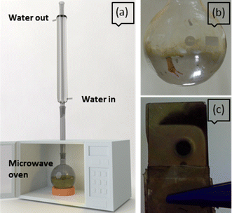 | ||
| Fig. 1 (a) Schematic of the experimental setup with modified microwave oven (b and c) mirror like appearance inside a round-bottom flask and on glass substrate, respectively, due to Ag deposition. | ||
| Sample code | Substrate | AgNO3 concentration (mM) | Deposition time (s) |
|---|---|---|---|
| A | Unpatterned aluminum | 10 | 90 |
| B | Glass | 10 | 90 |
| C | Glass | 500 × 10−3 | 90 |
| D | Nano-patterned aluminum (NPA) | 10 | 90 |
| E | NPA | 500 × 10−3 | 90 |
| F | NPA | 20 × 10−3 | 90 |
| G | NPA | 10 × 10−3 | 90 |
| H | NPA | 2 × 10⁻³ | 90 |
| I | Si (100) | 10 | 90 |
| J | Si (100) | 500 × 10−3 | 90 |
| K | Si (100) | 20 × 10−3 | 90 |
| L | Si (100) | 10 × 10−3 | 90 |
| M | Si (100) | 2 × 10⁻³ | 90 |
2.3 Characterization of substrates with silver nanoparticles
The coatings of AgNPs on different substrates were analyzed by X-ray diffraction (Rigaku Ultima-IV powder diffractometer, Cu Kα radiation). The surface morphology of the coatings was studied using scanning electron microscopy (Zeiss Gemini Ultra 55 Field Emission SEM, equipped with an energy-dispersive X-ray spectrometer). The reflectivity of the coatings was characterized by spectrophotometry (PerkinElmer Lambda 950 spectrophotometer with a 150 mm integrating sphere attachment).3. Results and discussion
Aluminum substrates were electropolished before carrying out anodization in order to reduce their surface roughness. Fig. 2a shows the oxide layer formed on aluminium during electrochemical anodization, revealing the disordered arrangement of pores. A highly ordered pattern resembling a hexagonal honeycomb-like structure was obtained after the oxide layer was etched away (Fig. 2b). Decorating metal nanoparticles on such “nano-patterned” surfaces is beneficial in various applications.21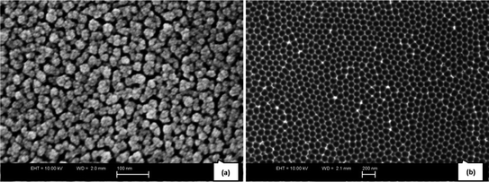 | ||
| Fig. 2 FESEM images of (a) aluminium oxide layer on the anodized aluminium substrate and (b) nano-patterned aluminium substrate after oxide removal. | ||
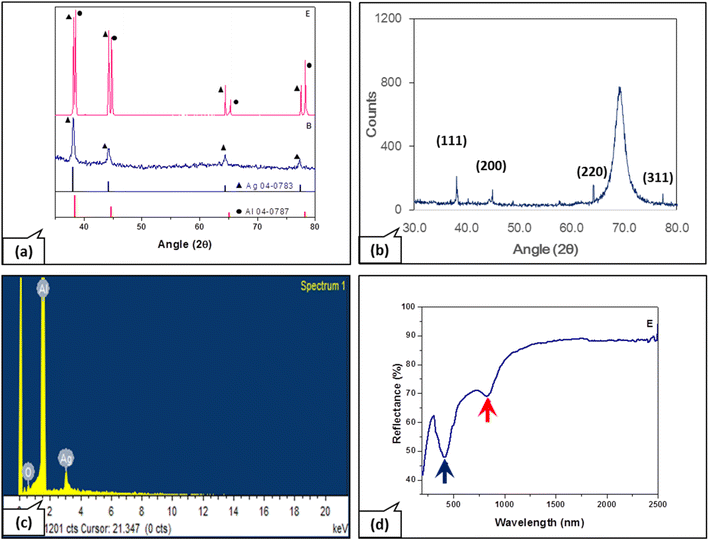
The deposition of AgNP on unpatterned aluminium, nano-patterned aluminium, and glass substrates was carried out using MAST. The X-ray diffractogram of the deposit on an aluminum substrate (sample E) reveals the cubic pattern characteristic of silver (a = 4.09 Å, Fm3m, JCPDS number 04-0783) (Fig. 3a).22 The peaks at 2θ = 38.12°, 44.28°, 64.43°, 77.48°, and 81.54° may be assigned, respectively, to the (111), (200), (220), (311) and (222) planes of fcc silver. The broad peaks are indicative of the small crystallite size. In the case of sample B, a deposit on a glass substrate, there are no peaks other than those due to Ag, indicating the purity of the silver material. XRD pattern of Ag on silicon substrate (Fig. 3b), showed similar silver peaks. The peak at 69° is due to the silicon substrate. The presence of Ag was also confirmed by EDS microanalysis (Fig. 3c). Traces of oxygen seen in the EDS pattern are attributable to the native oxide on Al or traces of the reducing agent used in our study. No signs of any other elements confirm the material purity displayed by two-dimensional elemental maps. However, in the case of sample E, Al substrate peaks (a = 4.05 Å, Fm3m, JCPDS number 04-0787) are observed, in addition to Ag peaks. Thus, the deposition conditions corresponding to sample E are conducive to obtaining uniform and well-distributed AgNP for desired applications. The reflectance spectrum of sample E was collected with near-normal incidence and reflectance angle of 8°. The local minimum in the reflectance spectrum around 825 nm (red arrow in Fig. 3d) is due to the significant inter-band transition around 1.5 eV for aluminum.23,24 The reduced reflectance intensity around 420 nm (blue arrow in Fig. 3d) is due to absorption by AgNPs, confirming their presence on the aluminum substrate.
Deposition at high precursor concentration (sample A) led to thick and dense deposits. The colorless reaction mixture turned pale yellow during microwave irradiation, and the substrate appearance changed to yellowish, indicating the formation/deposition of silver. In addition to a uniform deposition on the immersed substrate, a mirror-like coating on the inner wall of the glass container could be readily discerned (Fig. 1b and c). FESEM imaging reveals the near-spherical morphology of the “grains” comprising the deposit, each “grain” being an agglomeration of nanoparticles (Fig. 4a) ranging in size from ∼30 nm to ∼300 nm (Fig. 4b).
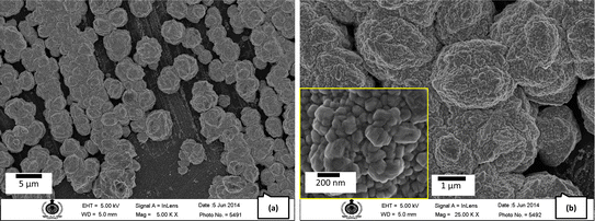 | ||
| Fig. 4 FESEM images of silver nanoparticles on an unpatterned Al substrate (sample A) at (a) lower magnification and (b) higher magnification (inset shows a magnified view). | ||
Deposition on glass substrates at the highest concentration (sample B) led to mirror-like coatings, whereas no mirror-like appearance could be observed for lower concentrations. The appearance of glass substrates changed from silver to brown upon reducing the concentration of AgNO3. The deposition was uniform and spread over the entire substrate, as can be seen from the FESEM image (Fig. 5a). The magnified image shows nearly spherical nanoparticles of various sizes centered about 80 nm, as seen from the histogram (Fig. 5b). At a concentration of 500 μM (sample C), a sparing deposition of spherical nanoparticles with reduced particle size occurred (Fig. 7f).
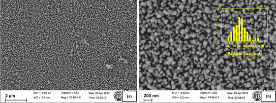 | ||
| Fig. 5 FESEM images of silver nanoparticles on glass substrate (sample B), at (a) lower magnification and (b) higher magnification (inset shows histogram of particle sizes). | ||
Nano-patterned aluminium (NPA) was also used as a substrate for the deposition of AgNP, and the effect of precursor concentration on the deposition was studied (samples D–H). To achieve narrow size distribution and uniform separation of particles, which are essential for plasmonic applications, we also attempted deposition at low precursor concentrations. In sample D, obtained at high precursor concentration, large “chunks” were observed, in addition to much smaller nanoparticles (Fig. 6a). At 500 μM concentration, nearly spherical nanoparticles (∼70 nm) and their agglomerates were observed (Fig. 6b). When the concentration was reduced to 20 μM (a factor of 500), the particle size was reduced with nearly spherical shapes (sample F, Fig. 6c). However, the amount of deposits was still high. The deposit was dense, which suggested the need for further fine-tuning the deposition conditions. A concentration of 10 μM appears to be optimum in that deposition of nearly mono-disperse particles (∼50 nm) decorates the hexagonal pattern of the NPA conformally (sample G). It may be seen that such nanoparticles are also deposited in the “wells” of the hexagonal pattern (Fig. 6d). The protruding edges of the hexagonal pattern on the substrate appear to act as nucleation sites. Hence, the density of nanoparticles is higher on the pore edges. In contrast, the density of silver nanoparticles in the concave “dimples” is lower (Fig. 6e). This is attributable to the effect of the applied microwave field: it is surmised that the effect of the associated electric field is more significant at the sharp edges of the pores in the metal than in the “wells”. The larger average size of the particles on the pore edges may also be a consequence of the same. Further dilutions (2 μM and lower) did not yield uniform deposition, as can be seen by the reduced density of AgNP (Fig. 6f). It is likely that, at such low concentrations, much more prolonged exposure to microwave radiation is needed to obtain uniform deposition. Two-dimensional elemental maps of sample E (Fig. S1, ESI†) show a uniform distribution of silver throughout the surface of the aluminium substrate.
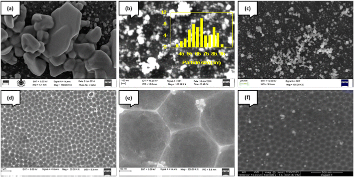 | ||
| Fig. 6 FESEM images of silver nanoparticles on nano-patterned aluminium (a) sample D, (b) sample E, (c) sample F, (d) sample G, (e) sample G-magnified view, and (f) sample H. | ||
Silicon substrates were used for the deposition of AgNP employing varying precursor concentrations (samples I–M, Table 1). Sample I, obtained with the highest concentration, displays heaps (islands) of Ag measuring about 20 μm in the extension, each comprising platelets ∼100 nm in thickness and several μm across (Fig. 7a). At 500 μM concentration, there is a lot of Ag deposition with a broad particle size distribution (Fig. 7b). As the concentration was reduced sharply to 20 μM (sample K), silver nanocrystals of various sizes and shapes were formed, some as large as ∼400 nm (Fig. 7d). Many have polyhedral shapes characteristic of the cubic structure of silver, suggesting crystal growth under equilibrium-like conditions (Fig. 7c, inset). When the concentration was further reduced to 10 μM (sample L), crystals were even larger, measuring up to 1 μm; these crystals also are faceted, characteristic of growth under equilibrium conditions (Fig. 7d). Sample M, obtained from a solution with a concentration of 2 μM, shows the formation of silver crystals, which is visibly sparser than at higher concentration samples. This is clearly due to the very low concentration of the precursor in the solution. The AgNP are distributed quite uniformly over the surface of the silicon substrate, with a relatively narrow size distribution centered at ∼30 nm (Fig. 7e).
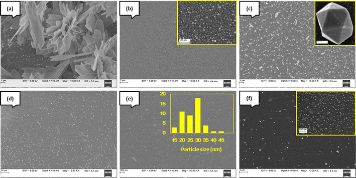 | ||
| Fig. 7 FESEM images of silver nanoparticles on Si (100) (a) sample I, (b) sample J, (c) sample K, (d) sample L, (e) sample M, and (f) glass substrate (sample C). | ||
A few inferences can be drawn from the results on the deposition of silver on different substrates from a microwave-irradiated solution. The nucleation density is high at high precursor concentrations, resulting in considerable agglomeration of nanoparticles, as seen on an aluminum substrate. Agglomeration of a different kind occurs on silicon, where “heaps” of silver platelets – presumably single-crystalline – are formed. Very limited agglomeration occurs on glass, where a uniform coating of fairly monodisperse nanocrystals of silver occurs, resulting in a mirror-like appearance. It is surmised that the differences arise from the substrate's interaction (or lack thereof) with the microwave field. Deposition on glass, which is transparent to microwaves, shows no agglomeration of the silver nanocrystals nucleated from the irradiated solution and deposited on it. The intense interaction between the microwave field and the highly conducting aluminium (3.7 × 10⁵ S cm−1) leads to significant agglomeration/fusion of silver nuclei at the substrate surface.
At the highest precursor concentration, there is agglomeration on both Al and Si substrates, though the morphologies are different. The difference can be understood on the basis of the different dielectric response of the substrate to the incident microwaves in the two cases. Al is opaque to microwaves, but the top layer (on both sides of the substrate) absorbs microwaves (skin effect), which leads to the heating of the substrate. That causes the nuclei formed on Al to be mobile and they merge to form large islands around each center of initial nucleation. So, the islands are rather “flat”. That is, their thickness is less than their diameter.
Doped silicon has much lower conductivity (0.1 S cm−1) than aluminum, due to which nucleation and growth of silver occur in a manner that – somehow – leads to the formation of thin but sizeable platelets. A detailed study would be required to understand how platelets are formed on doped Si (100) substrates. The Si substrate was of device-grade and doped (p-type, with resistivity of 10 ohm cm). Such a substrate absorbs microwaves and gets heated under irradiation. However, the thermal conductivity of doped Si is much less than that of Al, which means that the nuclei formed at a high concentration cannot move along the substrate as much as they can on the surface of Al with its high thermal conductivity. So, the growth of the silver being deposited occurs in a direction rather perpendicular to the substrate, with Ag particles that are formed moving on the previously formed Ag surfaces, given the very high thermal conductivity of Ag. Such mobility is aided by the heating of the thin deposits of Ag, due to absorption of the incident microwave irradiation. Thus, the difference between the morphologies of the Ag deposited at the same concentration on Al and Si arises from the differences in the dielectric response and thermal conductivity.
At a much lower precursor concentration, the possibility of agglomeration is reduced (on all substrates) because of the reduced nucleation density. However, the interaction of the substrate with the microwave field continues to be a factor. As a result, the deposit on aluminum comprises mostly spherical or shapeless silver particles, whereas the silver particles deposited on silicon are well-formed and faceted. Thus, microwave-assisted deposition on conducting substrates is a complex process, especially when the deposit itself is a very good metal like silver. The metal particles already nucleated are likely to complicate the interactions further.
The salient features of the MAST method include (1) rapid (90 s) deposition of AgNP; (2) substrate-specific deposition; (3) not limited by substrate dimensions; (4) conformal deposition; (5) simplicity and economy of time and effort; (6) control of the deposits. To the best of our knowledge, microwave-assisted deposition of AgNP has not been reported. The rapid deposition stems from the capability of microwaves to produce efficient and effective heating of the solution at the molecular level, resulting in chemical reactions and nucleation occurring very quickly.16 Additionally, the substrate (if it is not a conductor) is also heated by irradiation, facilitating the decomposition of the precursor at the substrate surface, which leads to conformal deposition. Our results suggest that careful optimization of solution concentration and reaction times can be used to tailor the quality of Ag deposition.
4. Conclusions
A novel, low-cost, and rapid one-pot method for depositing silver nanoparticles using microwave irradiation of aqueous silver nitrate was developed. Silver nanoparticles could be uniformly deposited on various substrates within just 1.5 min. The concentration of silver nitrate plays a significant role in controlling the growth of nanoparticles and their inter-particle spacing. A concentration of 10 μM was optimum for obtaining ∼50 nm particles conformally deposited on nano-patterned aluminium. The AgNPs were found to decorate the pore edges of the highly ordered hexagonal patterns of the nano-patterned aluminium. For silicon substrates, 2 μM concentration provided the uniformly distributed spherical AgNPs of size ∼30 nm. The microwave irradiation-based approach, being versatile and robust, provides a simple and elegant way of creating substrates decorated by AgNPs, with the capability for large-area deposition, which could be helpful in various surface-enhanced spectroscopies, catalysis, and sensing applications.Data availability
The data supporting this article have been included as part of the ESI.†Conflicts of interest
There are no conflicts to declare.Acknowledgements
We gratefully acknowledge (i) financial support from SERB, DST Govt. of India through projects no. SB/FT/CS-123/2013 and SB/S2/CMP-017/2014 (ii) the joint financial support by Manipal Academy of Higher Education and DST-FIST, Govt. of India Program via approval letter SR/FST/PSI-174/2012.References
- V. A. Kumar, Y. Nakajima, T. Uchida, T. Hanajiri and T. Maekawa, Synthesis of nanoparticles composed of silver and silver chloride for a plasmonic photocatalyst using an extract from needles of Pinus densiflora, Mater. Lett., 2016, 176, 169–172 CrossRef CAS.
- R. Krajcar, J. Siegel, O. Lyutakov, P. Slepička and V. Švorčík, Optical response of anisotropic silver nanostructures on polarized light, Mater. Lett., 2014, 137, 72–74 CrossRef CAS.
- U. Mandi, A. S. Roy, S. K. Kundu, S. Roy, A. Bhaumik and S. M. Islam, Mesoporous polyacrylic acid supported silver nanoparticles as an efficient catalyst for reductive coupling of nitrobenzenes and alcohols using glycerol as hydrogen source, J. Colloid Interface Sci., 2016, 472, 202–209 CrossRef CAS PubMed.
- Q. Zhou, S. Wang, N. Jia, L. Liu, J. Yang and Z. Jiang, Synthesis of highly crystalline silver dendrites microscale nanostructures by electrodeposition, Mater. Lett., 2006, 60(29–30), 3789–3792 CrossRef CAS.
- S. Yallappa, J. Manjanna and B. L. Dhananjaya, Phytosynthesis of stable Au, Ag and Au–Ag alloy nanoparticles using J. Sambac leaves extract, and their enhanced antimicrobial activity in presence of organic antimicrobials, Spectrochim. Acta, Part A, 2015, 137, 236–243 CrossRef CAS PubMed.
- K. Ray, M. H. Chowdhury and J. R. Lakowicz, Aluminum nanostructured films as substrates for enhanced fluorescence in the ultraviolet-blue spectral region, Anal. Chem., 2007, 79(17), 6480–6487 CrossRef CAS PubMed.
- M. Manzano, P. Vizzini, K. Jia, P.-M. Adam and R. E. Ionescu, Development of localized surface plasmon resonance biosensors for the detection of Brettanomyces bruxellensis in wine, Sens. Actuators, B, 2016, 223, 295–300 CrossRef CAS.
- B. Cerjan, X. Yang, P. Nordlander and N. J. Halas, Asymmetric aluminum antennas for self-calibrating surface-enhanced infrared absorption spectroscopy, ACS Photonics, 2016, 3(3), 354–360 CrossRef CAS.
- Y. Zhao, Y. J. Zhang, J. H. Meng, S. Chen, R. Panneerselvam and C. Y. Li, et al., A facile method for the synthesis of large-size Ag nanoparticles as efficient SERS substrates, J. Raman Spectrosc., 2016, 662–667 CrossRef CAS.
- S. Iravani, H. Korbekandi, S. V. Mirmohammadi and B. Zolfaghari, Synthesis of silver nanoparticles: chemical, physical and biological methods, Res. Pharm. Sci., 2014, 9(6), 385–406 CAS.
- S. Brahma and S. Shivashankar, Microwave irradiation-assisted method for the deposition of adherent oxide films on semiconducting and dielectric substrates, Thin Solid Films, 2010, 518(21), 5905–5911 CrossRef CAS.
- S. Komarneni, R. Roy and Q. Li, Microwave-hydrothermal synthesis of ceramic powders, Mater. Res. Bull., 1992, 27(12), 1393–1405 CrossRef CAS.
- I. Bilecka, M. Kubli, E. Amstad and M. Niederberger, Simultaneous formation of ferrite nanocrystals and deposition of thin films via a microwave-assisted nonaqueous sol–gel process, J. Sol-Gel Sci. Technol., 2011, 57(3), 313–322 CrossRef CAS.
- S. G. Menon, K. S. Choudhari, S. A. Shivashankar, S. Chidangil and S. D. Kulkarni, Microwave solution route to ceramic ZnAl2O4 nanoparticles in 10 minutes: inversion and photophysical changes with thermal history, New J. Chem., 2017, 41(13), 5420–5428 RSC.
- S. G. Menon, K. S. Choudhari, S. A. Shivashankar, C. Santhosh and S. D. Kulkarni, Thermal effects on rapid microwave synthesized Co:ZnAl2O4 spinel nanoparticles, J. Alloys Compd., 2017, 728, 1083–1090 CrossRef CAS.
- I. Bilecka and M. Niederberger, Microwave chemistry for inorganic nanomaterials synthesis, Nanoscale, 2010, 2(8), 1358–1374 RSC.
- K. S. Choudhari, P. Sudheendra and N. Udayashankar, Fabrication and high-temperature structural characterization study of porous anodic alumina membranes, J. Porous Mater., 2012, 19(6), 1053–1062 CrossRef CAS.
- K. S. Choudhari, P. Jidesh and N. Udayashankar, Fabrication of nanoporous alumina and their structural characteristics study using SEM image processing and analysis, Synth. React. Inorg., Met.-Org., Nano-Met. Chem., 2012, 42(3), 369–375 CrossRef CAS.
- K. S. Choudhari, P. Jidesh, P. Sudheendra and S. D. Kulkarni, Quantification and morphology studies of nanoporous alumina membranes: a new algorithm for digital image processing, Microsc. Microanal., 2013, 19(04), 1061–1072 CrossRef CAS PubMed.
- R. Sai, S. D. Kulkarni, K. Vinoy, N. Bhat and S. Shivashankar, ZnFe2O4: rapid and sub-100 C synthesis and anneal-tuned magnetic properties, J. Mater. Chem., 2012, 22(5), 2149–2156 RSC.
- M. Fan, G. F. S. Andrade and A. G. Brolo, A review on the fabrication of substrates for surface enhanced Raman spectroscopy and their applications in analytical chemistry, Anal. Chim. Acta, 2011, 693(1), 7–25 CrossRef CAS PubMed.
- K. S. Choudhari and S. D. Kulkarni, Development of novel deposition method for silver nanostructures on flexible and nanopatterned surfaces, Procedia Mater. Sci., 2014, 5, 1043–1048 CrossRef CAS.
- S. D. Kulkarni, K. S. Choudhari and C. Santhosh, Optical Interferometric Properties of Iridescent Nanoporous Anodic Alumina, Procedia Mater. Sci., 2014, 5, 988–994 CrossRef CAS.
- Y.-C. Tsao, T. Søndergaard, E. Skovsen, L. Gurevich, K. Pedersen and T. G. Pedersen, Pore size dependence of diffuse light scattering from anodized aluminum solar cell backside reflectors, Opt. Express, 2013, 21(101), A84–A95 CrossRef CAS PubMed.
Footnote |
| † Electronic supplementary information (ESI) available. See DOI: https://doi.org/10.1039/d4ra03132f |
| This journal is © The Royal Society of Chemistry 2024 |

