 Open Access Article
Creative Commons Attribution 3.0 Unported Licence
Photovoltaic properties of halide perovskites for solar cell application with efficiency greater than 18%
Shahid Mehmood *a,
Numan Khana,
Zahid Ali
 *a,
Imad Khan
 a and
Sarah Abdullah Alsalhib
aDepartment of Physics, University of Malakand Chakdara, Dir 18800, Pakistan. E-mail: Zahidf82@gmail.com; shahiduom07@gmail.com
bCollage of Science, Department of Physics, Princess Nourah bint Abdulrahman University, Riyadh, Saudi Arabia
First published on 24th September 2024
Abstract
The opto-electronic properties and solar cell efficiency of halide perovskites A2LiInBr6 (A = Rb, Cs) are investigated using density functional theory (DFT) through WEIN2k and SCAPS-1D. The electronic characteristic of A2LiInBr6 (A = Rb, Cs) compounds reveal their direct bandgap semiconductor nature and are active in visible rang. The results indicate that substituting Cs with Rb causes a slight narrowing of the bandgap. According to the optical analysis, these compounds possess dynamic visible-range optical properties that make them ideal for application in opto-electronic devices and solar cells. The A2LiInBr6 (A = Rb, Cs) absorber layer is employed to simulate the solar cell efficiency of these lead free perovskite-based device. The optimized FTO/WS2/A2LiInBr6 (A = Rb, Cs)/Spiro-MeOTAD/Cu solar cells exhibit the best performance with WS2 as the ETL and Spiro-MeOTAD as the HTL having Voc value of 2.27 V and 1.85 V, Jsc value is 11.35 and 11.44 mA cm−2, FF is 73.24% and 83.84%, PCE is 18.88% and 17.97%, Rs is 9.94 and 4.88 Ω cm2 and Rsh is 1.35 and 1.14 Ω cm2 respectively. As a result, this research paves the way for future experiments to create entirely inorganic perovskite photovoltaics, free of lead toxicity and exhibit improved photovoltaic ability.
1. Introduction
Perovskites, especially double perovskites, have shown great promise in various applications such as solar cells (SCs), light emitting diodes (LEDs), ferroelectrics, photo detectors, electro catalysts, nano-lasers, magneto resistive materials, white light emitters, and spintronics.1–8 A lot of the uses of perovskites depend on stability over the long term and inorganic materials are prominent for their robust stability in both air and water, hold significant attraction and promise across various applications.9 Numerous applications in optoelectronics, like single junction solar cells are preferably designed with band gaps that align well with the near infrared spectrum. Conversely, most perovskites and double perovskites identified to date show metallic properties or have band gaps within the visible range. Consequently, it is imperative to fabricate new types of perovskites materials, particularly double perovskites with lower band gaps, to facilitate the implementation of numerous practical devices.Improvements in perovskite solar cells have been dramatic over the last several decades, with efficiency jumping from 3.8% in 2009 to a whopping 22.7% in 2017-all under controlled laboratory conditions.10–13 Researcher has shown interest in the latest developments in halide perovskites, especially inorganic-lead halide perovskites like CH3NH3PbI3, because of their amazing optical and photovoltaic properties.14 However, issues like lead toxicity and long-term stability concerns hinder the practical use of these materials, hence research into lead-free alternatives is necessary. Exceptional optoelectronic characteristics, low cost, and ease of recycling are required of these substitutes. In addition to competing with existing PV technologies, they also need to fulfill commercial needs including scalability, stability, reliability, and flexibility.15–17
In response to these concerns, there has been considerable effort to replace lead-based perovskites with more eco-friendly perovskites based on lead-free halides. The exceptional optoelectronic characteristics of semiconducting halide double perovskites, such as high optical absorption coefficient, elevated carrier mobility, tunable bandgap, minimal electron–hole effective masses, and extensive molar extinction coefficient, have garnered significant interest from materials scientists. Consequently, lead-free alternatives have emerged as a important point in both theoretical and experimental investigations, owing to their stability and potential applications in optoelectronic devices.18–20
Due to the exceptional optoelectronic capabilities of the lead-free alternatives, it have shown an effective replacement. First-principles approaches have extensively explored detailed combinations of elements such as Li, K, Na, Cs, In, Ag, Bi, Sb, and halogens within the framework of double perovskites research. These studies line up understanding the diverse uses and potential effectiveness of these compounds.21–24 Compounds synthesized by combining of Li, Na K with Ga, In and Tl have recently gained attention because to their advantageous electron–hole carrier mobility characteristics, direct band gap features, and intrinsic stability. Furthermore, significant research accomplishments have focused on first-principles methods to explore lead free perovskites such as Cs2InGaX6 (X = Cl, Br, or I),25 Cs2MGaBr6 (M = Li, Na),26 A2KGaI6 (A = Cs, Rb),27 Rb2GaInX6 (X = Cl, Br, I),28 Rb2XGaBr6 (X = Na, K)29 and Cs2AgSb1−xGaxI6.30 Recently Luo et al.31 and Sun et al.32 studied the Li-based double perovskites, Cs2LiInX6 (X = F, Cl, and Br), Rb2LiInBr6, Cs2B′In0.75Bi0.25I6 (B′ = Li, Na and K), and reported that these compounds have certain application in optoelectronic devices, additionally their modest electron–hole carrier mass, direct band gap properties thermal and dynamic stability make them excellent candidates for use in optoelectronics and transport dynamics. The investigations highlight the remarkable optical performance of these materials in the visible spectrum, which is influenced by their structural stability and optimum band gap values and possibly applicable for a variety of applications. This study uses DFT calculations to understand how Li-base halide double perovskites, behave when they absorb light. Specifically, the investigation focuses on the A2LiInBr6 (A = Rb, Cs) compounds, aiming to study their potentials like electrical characteristics, light-harvesting capabilities, optical features and (SC) performance.
2. Computational detail
The WIEN2k package,33 which utilizing the full potential linear augmented plane wave (FP-LAPW) methods to simulate the optoelectronic properties of A2LiInBr6 (A = Rb, Cs) within DFT.34 To improve results while using minimal computational means, various approaches have been tried to deal with exchange–correlation functionals, these contain Generalized Gradient Approximation (GGA),35 Tran and Blaha modified Becke–Johnson potential (TB-mBJ)36 and Perovskites mBJ (P-mBJ).37 In the FP-LAPW method, a muffin-tin (MT) sphere and interstitial region are usefully designed and employ these constructions to serve the essential function of containing charges within the system and stop charges from escaping. In this arrangement, the configuration of the harmonic expansion is determined within a muffin-tin sphere having RMT = 10/KMax, near LMax = 10. The force convergence criterion is set to 1 mRy Bohr−1, ensuring accurate structural optimization, while the expected energy difference between iterations is fine-tuned to 0.1 mRy, promoting stability in the calculation process. To adequately sample the Brillouin zone, a dense 13 × 13 × 13 grid of K-points is employed, enabling comprehensive coverage of electronic states. Furthermore, the optical properties of these compounds are rigorously determined using the Kramers–Kronig relation, ensuring accurate characterization of their optoelectronic behavior.WIEN2k is mostly used for electronic structure calculations but has some limitations when it comes to simulating solar cells. Amorphous or disordered materials, which are common in thin-film solar cells, are challenging to accurately model within the WIEN2k framework. Modeling heterojunctions, which are essential for many high-efficiency solar cells, can be computationally demanding and less straightforward in WIEN2k. SCAP1D on the other hand is more suitable option for solar cell simulations as it is specifically designed to model the electrical behavior of semiconductor devices, including solar cells. It can handle heterojunctions and other complex device structures. SCAP1D can often be coupled with electronic structure codes like WIEN2k to obtain material parameters for more accurate simulations. WIEN2k and SCAP1D are complementary tools. WIEN2k provides fundamental material properties, which SCAP1D can then use to simulate device performance. Combining these tools can result in more accurate and comprehensive solar cell modeling, therefore in the current study the SCAP1D is used to estimate the solar cell parameters for the understudy compounds.
The simulation of the solar cell device, composed of FTO/WS2/A2LiInBr6 (A = Rb, Cs)/CBTS/Cu, is conducted under carefully controlled parameters. Illumination is provided by a light source featuring an A.M. 1.5 spectrums with an intensity of 1000 mW cm−2, replicating standard solar irradiance conditions. The simulated temperature is held constant at 300 K to mimic typical operating environments. Dynamic processes within the device are accurately modeled by setting the frequency of the simulation to 1 × 616 Hz. A scanning voltage range spanning from 0 to 1.50 V is employed to comprehensively assess the device's performance under varying operating conditions. These simulations are executed using SCAPS-1D, a robust software tool renowned for its effectiveness in modeling and optimizing solar cells.38 The parameters for electron transport layer (ETL), hole transport layer (HTL) are taken from ref. 39 and 40 and summarized in Table 1 along with absorber layer, the interface flaws between the absorber/HTL and absorber/ETL are described in Table 2 and the parameters used for electrode is summarize in Table 3. There is an assumption that there is no reflection of light on any surfaces or contacts. It is stated that the defect is singular, with a characteristic energy value of 0.1 eV.41,42
| Parameters | FTO | WS2 (ref. 39) | A2LiInBr6 | Spiro-MeOTAD40 |
|---|---|---|---|---|
| Thickness (nm) | 500 | 195 | 800 | 200 |
| Eg (eV) | 3.5 | 1.8 | 3.13, 3.01 | 3 |
| χ (eV) | 4.0 | 3.95 | 2.6 | 2.2 |
| εr | 9.0 | 13.6 | 3.19, 3.32 | 3.0 |
| Nc (cm−3) | 1019 | 1018 | 1022 | 2.2 × 10¹⁸ |
| Nv (cm−3) | 1019 | 1018 | 3.1 × 10²¹ | 1.8 × 10¹⁹ |
| VTh,e (cm s−1) | 107 | 107 | 107 | 107 |
| VTh,h (cm s−1) | 107 | 107 | 107 | 107 |
| μe (cm2 V s−1) | 5 × 101 | 5 × 10² | 9.74 × 10² | 2.1 × 10⁻³ |
| μh (cm2 V s−1) | 5 × 101 | 5 × 10² | 2.1 × 10² | 2.16 × 10⁻³ |
| ND (cm−3) | 1015 | 7.25 × 10¹⁸ | 0 | 0 |
| NA (cm−3) | 0 | 0 | 1019 | 1018 |
| NT (cm−3) | 1015 | 1015 | 1015 | 1015 |
| Parameters | Absorber | ETL/absorber | Absorber/HTL |
|---|---|---|---|
| Type of defect | Neutral | Neutral | Neutral |
| Cross section for electron (cm2) | 1 × 10⁻¹⁵ | 1 × 10⁻¹⁵ | 1 × 10⁻¹⁵ |
| Cross section for electron (cm2) | 1 × 10⁻¹⁵ | 1 × 10⁻¹⁵ | 1 × 10⁻¹⁵ |
| Energetic distribution | Single | Single | Single |
| Energy level with respect to Ev (eV) | 0.6 | 0.65 | 0.65 |
| Characteristic energy (eV) | 0.1 | 0.1 | 0.1 |
| Total density (cm−3) | 1014 | 1 × 10¹⁵ | 1 × 10¹⁵ |
| Contacts | Back metal contact properties | Back metal contact properties |
|---|---|---|
| Metal work function | 5.0 | 4.56 |
| Surface recombination velocity of electron (cm s−1) | 1 × 10⁷ | 1 × 10⁷ |
| Surface recombination velocity of electron (cm s−1) | 1 × 10⁵ | 1 × 10⁵ |
3. Results and discussion
3.1 Electronic properties
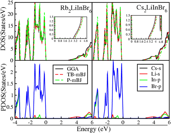
Many physical characteristics of compounds are associated to their electronic band structure. As per the literature, each compound possesses a distinct set of electrical characteristics owing to the uniqueness of its band structure.The electrical properties of materials are related to their density of states (DOS), representing the distribution of available electronic states at various energy levels. Fig. 1 shows the total density of states (TDOS) obtained through different computational methods, including GGA, TB-mBJ, and P-mBJ. Notably, the Fermi level (EF) is standardized at 0 eV to accurately assess the TDOS for these compounds, offering a comprehensive understanding of their electronic structures and behavior. The TDOS reveals that the A2LiInBr6 (A = Rb, Cs) compounds are semiconductors; the valence band (VB) and conduction (CB) encompass the energy gap and EF does not cross by densities.
The bandgap values for these compounds were calculated in the current study using several potentials. The band gap value obtained by GGA, TB-mBJ and P-mBJ are 2.88, 3.02 and 3.13 eV for Rb2LiInBr6 and are 2.76, 2.89 and 3.01 eV for Cs2LiInBr6 respectively shown in Table 4. Other groups previously calculated the band gap of isotropic double perovskites compounds e.g. Cs2AlBiCl6, Cs2LiAlCl6, Cs2LiInBr6,Rb2AgGaCl6 and Cs2AgSbCl6 are 3.23 eV, 3.22 eV, 3.75 eV, 2.53 eV and 2.35 eV respectively.26,31,43 Cs and Rb are close enough that substituting one for the other won't significantly alter their structure or functionality. The features of these lead-free double perovskites in the current study are similar to those used as solar cell and are less hazardous than lead perovskites. The present study's comparative analysis of estimated band gaps shows good agreement with the band gap of available literature. This agreement confirms the accuracy of mBJ approach's in band gap estimation and due to its usefulness it is used throughout the calculation.
According to the literature, mBJ method is proving to be quite efficient and accurate in determining band gaps for semiconductors. By proposing results comparable to more expensive methods like hybrid functional or GW, while being cost-effective like LDA/GGA functionals, it presents a valuable option for researchers. The improved exchange potential, treatment of localization, and accurate description of dielectric properties. Additionally its ability to provide results closer to experimental values than other theoretical approaches is a significant advantage and seem to be a promising tool for treating semiconductor.36,37
The graphical interpretation of Total Density of States (TDOS) for both compounds shows that switching from Rb to cation Cs, the valence states moves towards higher energy is less compared to the movement of conduction states towards lower energy. These results confirm that, the band gap becoming narrower and more precisely tuned. This effect is attributed to the increase in Cs cations ionic radii. Therefore, the ionic radius of mentioned halide ions influences hybridization, that further leading to suppression in the simulated band gap. This suppression in the band gap presents a valuable advantage for practical device fabrication, as it occurs across a range of energy levels, providing versatility in optimizing device performance for various applications.44
The Partial Density of States (PDOS) calculations for the lead-free compounds A2LiInBr6 (A = Rb, Cs) is depicted in Fig. 1, which offers valuable insight into the semiconducting properties of these materials. In Fig. 1 the s state of Cs and Li and p state of In and Br displays clearly. The contribution of both Cs and Li ‘s’ states are negligible but most of the contribution is due to the p state of In and Br. The graph shows that in VB the p state of In and Br contribute mostly and are from −4 to zero eV while the contribution of the Li s state to the CB extends from the band gap to 6 eV correspondingly. The band gap occurs between the Br-p state and Li-s state in both compounds.
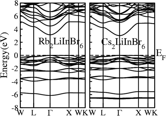
The calculated Electronic Band Structure (EBS) plotted across the irreducible Brillouin zone in K-space, specifically along high symmetry directions, for the A2LiInBr6 (A = Rb, Cs) compounds, that provides a detailed representation of the electronic properties of these materials presented in Fig. 2. The EBS analysis for these compounds confirms their semiconducting nature. Specifically the gamma symmetry point, where the VB maxima and CB minima meet signifies their behavior as direct band gap semiconductors. The calculated band gaps for A2LiInBr6 (A = Rb, Cs) compounds are 3.13 eV and 3.01 eV respectively by utilizing P-mBJ potential given is presented in Table 4. According to findings from another research group, the reported band gaps for these compounds are 2.6 eV and 2.2 eV, respectively, employing the mBJ potential.44 In Fig. 2, it's evident that the bandgap of the investigated compounds decreases as we switch from Rb to Cs. This trend is consistent with the substitution of cations with higher electronegativity for those with lower electronegativity. This phenomenon mirrors observations in other compounds, such as A3In2As4 and A5In2As6 (A = Sr and Eu), where the bandgap also decreases.45
3.2 Optical properties
Understanding the precise nature of interaction of light waves between these materials is of the utmost importance for opto-electronics applications. Here the optical properties are evaluated throughout an energy range of 0 to 14 eV has been carried out on these A2LiInBr6 (A = Rb, Cs) compounds. The optical factors computed in the current study are visualized in Fig. 3 and 4. These figures help us understand how light interacts with the materials we're studying, giving us a clear picture of their properties and behavior. The computed optical factors incorporate both the real part ε1(ω) and imaginary part ε2(ω) of the dielectric function, reflectivity R(ω), energy loss function L(ω), extinction coefficient k(ω), oscillator strength α(ω), refractive index n(ω), and optical conductivity σ(ω). These factors offer a thorough understanding of how light interacts with and characterizes the materials under investigation, providing valuable insights into their optical properties and behavior.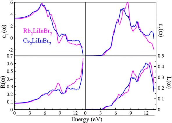 | ||
| Fig. 3 Dielectric function, reflectivity and loss function of the A2LiInBr6 (A = Rb, Cs) lead free halide perovskites. | ||
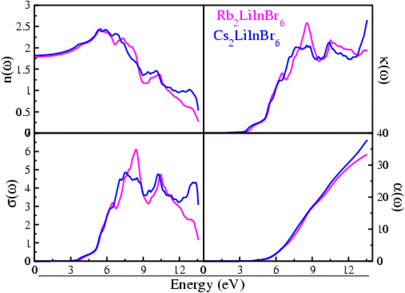 | ||
| Fig. 4 Refractive index, oscillator strength, excitation coefficient and optical conductivity of the A2LiInBr6 (A = Rb, Cs) lead free halide perovskites. | ||
The physical properties of the compound are described by the dielectric real part ε1(ω) are shown in In Fig. 3. The static dielectric constant, often denoted as ε1(0), represents the value of the dielectric function at zero electron volts (0 eV). This parameter provides crucial insight into the material's response to electric fields and its overall electronic structure. The static dielectric function ε1(0) provides insight into the material's polarization behavior, especially at low frequencies, reflecting the energy levels involved in external interactions. The calculated ε1(0) results for Rb2LiInBr6 and Cs2LiInBr6 compounds which are shown in Fig. 3, are 3.19 eV and 3.32 eV respectively. In A2LiInBr6, when A is switched from cation Rb to cation Cs, the value of ε1(0) increases while the band gap declines. This trend aligns strongly with Penn's model, which states that ε1(0) = 1 + [hωp/Eg].44 The simulated values of ε1 (0) and band gape (Eg) exhibit an inverse relationship, that confirming Penn's model. For A2LiInBr6 (A = Rb, Cs) compounds peaks arises at 5.45 and 5.29 eV, respectively, are observed in the spectra following at zero frequency. The spectra progressively flatten down up to become zero after this peak and eventually approach zero behaving like metal at those energies and no longer dielectric.
Fig. 3 illustrates the ε2(ω) values, indicating that there is no spectra present up to the optical gaps also listed in Table 3, which are 3.55 eV and 3.36 eV. The presence of multiple peaks in the imaginary dielectric function suggests that electronic excitations are influenced not just by energy levels but also by the calculated electronic properties of the material. These findings imply a deeper comprehension of the complicated relationship between electronic behavior and its manifestation in optical properties.
The calculated optical gap contracts when transitioning from Rb to Cs and are visible-light active, therefore suitable for solar cell application. The compounds A2LiInBr6 (A = Rb, Cs) in In Fig. 3 just after the threshold value, the curve begins to increase sharply, reaching peaks at 8.30 and 7.49 eV correspondingly, this enhanced understanding arises from significant interband transitions within the material.
The calculated reflectivity R(ω) for A2LiInBr6 (A = Rb, Cs) compounds is shown in Fig. 3 which is simply the fraction of reflected energy to incidental energy, serves to briefly reveal how a surface reacts to the incoming energy. As the 0 eV reflectance R(0) for A2LiInBr6 (A = Rb, Cs) compounds ranges from 7 to 8% respectively. The R(0) for Rb2LiInBr6 exhibits an extreme reflectivity of 67% at 13.56 eV, while for Cs2LiInBr6; the high reflectivity is 61% sharply at 13.6 eV. In the current study, as the energy approaches the point where the dielectric function ε1(ω) tends towards zero, there is a corresponding increase in reflectivity. This observation suggests that as the material's electronic properties align with certain energy levels, it becomes more reflective to incident light. The high reflectivity observed in the ultraviolet (UV) spectrum suggests that these compounds could serve effectively as a shield against high-frequency radiation.
The energy loss function, L(ω), which provides understanding into the energy dissipation of electrons pass through the material.46,47 Due to plasma frequency resonance, the studied compounds curves attain a maximum peak. Scattering does not occur where energy of photons is higher than the bandgap value, as seen in Fig. 3. Also Fig. 3 shows that the loss energy of the A2LiInBr6 (A = Rb, Cs) compounds extends from 9.10 to 13.07 eV, respectively, because of discrete energy bands.48
The n(ω) represent refractive index for the compounds understudy, presented in Fig. 4. For Rb2LiInBr6, the n(ω) value at zero frequency, that is n(0) is 1.78 although for Cs2LiInBr6, it is 1.82. After a certain point, the n(ω) real component starts to rise up to reaches its peak value, indicating the highest energy value which is 5.48 eV for Rb2LiInBr6 and 6.73 eV for Cs2LiInBr6.These compounds show significant refractive index n(ω) values, are a result of the limited passage of photons through the materials, indicating their substantial optical density.4
The material's ability to allow the passage of electrons when subjected to an electromagnetic field is quantified by its optical conductivity, denoted as σ(ω),which is presented in Fig. 4 for A2LiInBr6 (A = Rb, Cs) compounds, The σ(ω) initiates at the bandgap and progressively increases beyond it. A2LiInBr6 (A = Rb, Cs) compounds achieve their σ(ω) with respective values of 6.10 and 4.86 Ω−1 cm−1, as shown in Fig. 4.
The extinction coefficient is a measure of the interaction between a material and an electromagnetic wave, represented as k(ω).49–53 It's a practical conclusion that a material with a low k(ω) would exhibit excellent transmittance and minimal absorption.
The k(ω) values are predominantly zero up to the band gap, indicating minimal absorption and strong transmittance as demonstrated in Fig. 4. Maximum value for Rb2LiInBr6 is 1.72 at 8.55 eV and for Cs2LiInBr6 is 1.76 at 13.56 eV; these findings indicate that at these energy levels, both compounds exhibit high wave absorption and low wave transmission and is closely aligns with ε2(ω).
The oscillator strength, represented as α(ω), plays a crucial role in determining the number of electrons within the material that engage in an optical transition. As energy increases, the oscillator strength function α(ω), as shown in Fig. 4 for these compounds, also rises. The absence of occupied bands at lower energies can be attributed to the zero-sum rule. This principle indicates that the total number of electrons in the system remains constant; leading to the empty states in the unoccupied bands at lower energies. As here the bandgap narrows, there's a corresponding increase in the oscillator strength α(ω). As energy levels increase, there is a rapid escalation in the electron count within a system, starting from a zero baseline at lower energy states. The oscillator strength α(ω) analysis suggests that approximately 33–38 electrons participate in the optical transitions for the A2LiInBr6 (A = Rb, Cs) compounds, as observed from Fig. 4.
In summary, the distinguishing optical and electronic properties exhibited by these compounds underscore their promising suitability for utilization in solar cell technology.
3.3 Modelling and simulation of solar cell device
The optical properties exhibited by the investigated compounds prompt a deeper exploration of their potential as solar cell materials, particularly through an assessment of solar cell efficiency and current density (J) versus voltage (V) performances using the Solar Cell Capacitance Simulator (SCAPS – 1D).38 To assess the performance of solar cells constructed from several different double perovskites structures, we examine the impact of absorber layers and varying thicknesses of ETL. In this investigation, contour plot mapping is employed to assess key performance parameters of solar cells. The selection of an appropriate absorber material, HTL and ETL is crucial for attaining highest performance solar cells. By investigative contour plots representing efficiency, fill factor, open-circuit voltage, and short-circuit current density, researchers can identify optimal combinations of absorber, HTL and ETL materials that maximize solar cell performance. Additionally, selecting the appropriate thickness for the absorber, HTL and ETL is crucial for effectively capturing light and collecting holes generated within the absorber layer.In the proposed simulated structures, Ws2 and TiO2–SnO2 as taken as ETL and NiO, CuSCN, CuI, MoO3, WSe2, Spiro-MeOTAD and Cu2BaSnS4 denoted by (CBTS) as HTL, in addition Cu is used as a metallic back contact were tasted and the parameters including the short circuit current density (JSC), open circuit voltage (VOC), fill factor (FF), and PCE and the results are shown in Table 5.
| Devise structure | HTL | ETL | VOC (V) | JC (mA cm−1) | FF (%) | PCE (%) |
|---|---|---|---|---|---|---|
| FTO/NiO/absorber/WS2/Cu | NiO | WS2 | 1.31 (0.98) | 16.71 (17.59) | 78.26 (72.42) | 17.25, (12.49) |
| FTO/CuSCN/absorber/WS2/Cu | CuSCN | WS2 | 1.31 (0.98) | 16.64 (17.59) | 78.22 (72.42) | 17.17 (12.50) |
| FTO/CuI/absorber/WS2/Cu | CuI | WS2 | 1.31 (0.98) | 16.64(17.58) | 77.97 (72.43) | 17.11 (12.49) |
| FTO/MoO3/absorber/WS2/Cu | MoO3 | WS2 | 1.31 (0.98) | 16.64 (17.59) | 78.26 (72.43) | 17.29 (12.50) |
| FTO/WSe2/absorber/WS2/Cu | WSe2 | WS2 | 1.31 (0.98) | 16.72 (17.58) | 78.27 (72.43) | 17.27 (12.50) |
| FTO/Spiro-MeOTAD/absorber/WS2/Cu | Spiro-MeOTAD | WS2 | 2.27 (1.85) | 11.35 (11.44) | 73.24 (83.84) | 18.88 (17.97) |
| FTO/CBTS/absorber/WS2/Cu | CBTS | WS2 | 1.61 (1.53) | 16.41 (16.42) | 70.82 (71.44) | 18.77 (17.94) |
| FTO/CBTS/absorber/TiO2–SnO2/Cu | CBTS | TiO2–SnO2 | 1.23 (1.12) | 6.60 (12.89) | 84.39 (81.68) | 6.88 (11.81) |
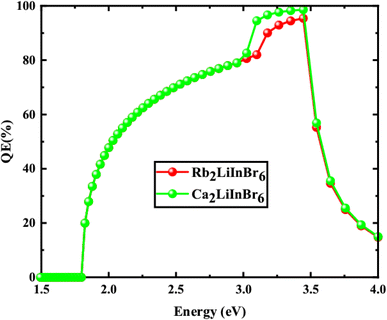
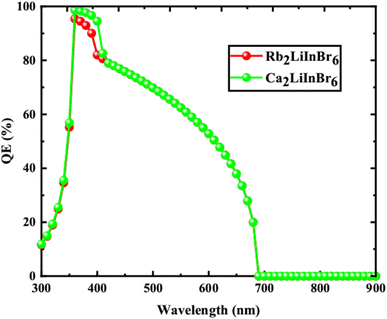
From the Table 5 the finest solar cell performance is attained for FTO/WS2/A2LiInBr6 (A = Rb, Cs)/Spiro-MeOTAD/Cu and their proposed structure as shown in Fig. 5. The quantum efficiency (QE) of a solar cell measures how effectively it converts incident photons into electron–hole pairs, expressed as the ratio of captured pairs to incident photons. These performance metrics are often characterized as functions of photon energy in electron volts (eV) or wavelength in nanometers (nm).54 The wavelength range from 300 to 900 nm and the photon energy range from 1.3 to 4.13 eV are utilized to measure the quantum efficiency (QE), as illustrated in Fig. 6 and 7, respectively. When using A2LiInBr6 compounds (A = Rb, Cs) as an absorber which is the key layer, the simulated device's quantum efficiency (QE) ranges from 11.67% to 11.98% at 4.1 eV (300 nm) and reaches 96 and 99% at 3.44–3.35 eV (360–370 nm) respectively and decreased to 19.96 and 19.98% at 1.82 eV (680 nm). Through careful analysis of the visible spectrum, the device is able to effectively convert photon energy into electrical energy. Nevertheless, the quantum efficiency (QE) reached to zero as the wavelengths become longer and the energy levels decrease. The HTL plays a crucial role in shaping the photovoltaic characteristics and hinders the movement of electrons, minimizing quenching losses by preventing effectively electron–hole (e–h) recombination and facilitating the drift of generated holes from the perovskite absorber layer to the back metallic contact, thereby enhancing power conversion efficiency (PCE).
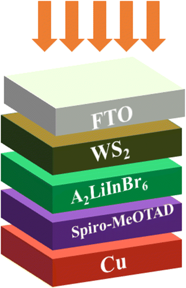 | ||
| Fig. 5 Schematic diagram of the solar cell device having A2LiInBr6 (A = Rb, Cs) lead free halide perovskites as a active layer. | ||
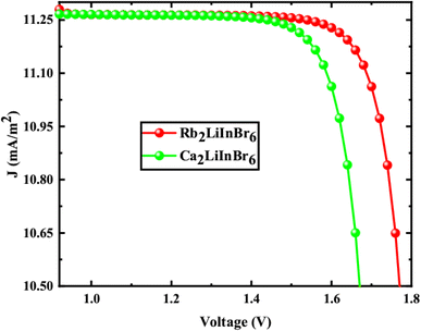
The solar cell parameters like VOC, JSC, FF, PCE, series resistance (Rs) and shunt resistance (Rsh) are obtained from the J–V shown in Fig. 8 for FTO/WS2/A2LiInBr6 (A = Rb, Cs)/Spiro-MeOTAD/Cu device, and the data is provided in Table 6, which is used to evaluate the photovoltaic (PV) characteristics.
| Parameters | Rb2LiInBr6 | Cs2LiInBr6 |
|---|---|---|
| VOC (V) | 2.27 | 1.85 |
| JC (mA cm−1) | 11.35 | 11.44 |
| FF (%) | 73.24 | 83.84 |
| PCE (%) | 18.88 | 17.97 |
| Rs | 9.64 | 4.88 |
| Rsh | 1.35 | 1.14 |
From the Table 6 the VOC is 2.27 V and 1.85 V, JSC is 11.35 and 11.44 mA cm−2, FF is 73.24% and 83.84%, PCE is 18.88% and 17.97%, Rs is 9.94 and 4.88 Ω cm2 and Rsh is 1.35 and 1.14 Ω cm2 correspondingly. When the bandgap of the active layer increases, it absorbs fewer photons, which in turn lowers the short-circuit current density (JSC). However, this also leads to an increase in the open-circuit voltage (VOC) because charge carriers segregate more easily within the active layer. These alterations have a significant impact on the overall power conversion efficiency (PCE) of the solar cell. As a consequence, the PCE of Rb2LiInBr6 is higher than that of the Cs2LiInBr6 base active layer.
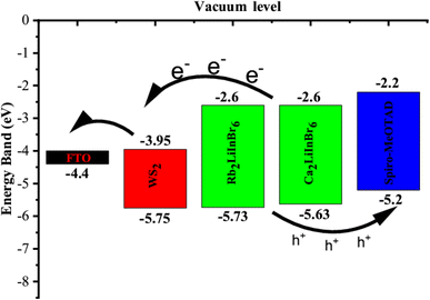
The valence band maxima (VBM) and conduction band minima (CBM) of the absorber, HTL and ETL layers are displayed in Fig. 9. The results demonstrate that the energy disparity between the absorber layer and the CBM of WS2 is less than that between the absorber layer and the VBM of WS2. Consequently, it promotes electron conduction from the absorber's conduction band to the FTO via the WS2 layer while inhibiting hole conduction from the absorber's VBM to the WS2 layer's VBM. In a similar vein, the energy disparity between the absorber layer's CBM and Spiro-oMeTAD is greater than the VBM's disparity with Spiro-MeOTAD. Due to these distinctions, holes can easily pass from the absorber's VBM to the Spiro-MeOTAD's VBM, but electrons can't pass from the absorber's CBM to the Spiro-MeOTAD's CBM.
Comparative study of the SCAPS-1D outcomes with reported work by using different double perovskites as an absorber layer is presented in Table 7. This comparison allows for an assessment of our work in relation to existing research. The table indicates that all the mentioned absorber layers did not achieve the awaited efficiency levels in previous studies. However, the current optimized device demonstrates significantly higher efficiency compared to previous works, highlighting the effectiveness of the current study. By integrating the optimized values obtained from this study with other reported results, it is observed that a substantial increase in the Power Conversion Efficiency (PCE) occur simulated in the current study. The previous reported PCE in Table 5 are 16.35%,55 1.965%,56 12%,43 10.30% (ref. 57) and 2.39% (ref. 58) while the PCE of the reported lead free absorber layer is 18.88 and 17. 97% respectively. This noteworthy improvement underscores the significance of this study in which environmentally friendly, Pb-free Perovskites Solar Cell (PSC) is designed, which incorporates inorganic charge transport layers.
4. Conclusions
The optoelectronic and photovoltaic characteristics of A2LiInBr6 (A = Rb, Cs) compounds are studied utilizing the FP-LAPW scheme in a DFT using GGA, TB-mBJ and P-mBJ potentials. Their band structure, total and partial densities of state calculations reveals that the A2LiInBr6 (A = Rb, Cs) are direct band gap semiconductors and the band gap values for A2LiInBr6 (A = Rb, Cs) drop from 3.13 to 3.01 eV when the cation is changed from Rb to Cs. The findings indicate that the examined materials exhibit optical dynamics within the visible range of the electromagnetic spectrum. This observation underscores their potential suitability for use as Solar Cell devices. The Solar Cell performance of device based on these perovskites is simulated by utilizing WS2 as the electron transport layer (ETL), Spiro-MeOTAD as the hole transport layer (HTL), and A2LiInBr6 (A = Rb, Cs) as absorber layer using SCAPS-1D. In the optimized FTO/WS2/A2LiInBr6 (A = Rb, Cs)/Spiro-MeOTAD/Cu solar cell structure, the achieved values are as follows: as VOC of 2.27 V and 1.85 V, JSC value is 11.35 and 11.44 mA cm−2, FF is 73.24% and 83.84%, PCE is 18.88% and 17.97%, Rs is 9.94 and 4.88 Ω cm2 and Rsh is 1.35 and 1.14 Ω cm2 respectively. For these reasons, our research covers the way for future experiments to develop inorganic lead-halide perovskites with enhanced photovoltaic performance.Data availability
The data used in the current study are available from the corresponding author on reasonable request.Conflicts of interest
The authors declare that they have no competing interest.Author contributions
Shahid Mehmood: investigation, methodology, writing – reviewing and editing, Numan khan: investigation, data curation, methodology, writing – original draft preparation, Zahid Ali: project administration, supervision, conceptualization, Imad Khan: visualization, formal analysis, reviewing and editing, Sarah Abdullah Alsalhi: funding acquisition, resources, software.Acknowledgements
Princess Nourah bint Abdulrahman University Researchers Supporting Project Number (PNURSP2024R453), Princess Nourah bint Abdulrahman University, Riyadh, Saudi Arabia.References
- S. H. Turren-Cruz, A. Hagfeldt and M. Saliba, Methylammonium-free, high-performance, and stable perovskite solar cells on a planar architecture, Science, 2018, 362, 449–453, DOI:10.1126/science.aat3583.
- E. K. Kim, S. G. Motti, R. Sorrentino and A. Petrozza, Enhanced solar cell stability by hygroscopic polymer passivation of metal halide perovskite thin film, Energy Environ. Sci., 2018, 11, 2609–2619, 10.1039/C8EE01101J.
- T. Leijtens, R. Prasanna, K. A. Bush, G. E. Eperon, J. A. Raiford, A. Gold-Parker, E. J. Wolf, S. A. Swifter, C. C. Boyd, H.-P. Wang, M. F. Toney, S. F. Bent and M. D. McGehee, Tin–lead halide perovskites with improved thermal and air stability for efficient all-perovskite tandem solar cells, Sustainable Energy Fuels, 2018, 2, 2450–2459, 10.1039/C8SE00314A.
- C. Duan, J. Tong, M. Shang, S. Nikodemski, M. Sanders, S. Ricote, A. Almansoori and R. O'Hayre, Readily processed protonic ceramic fuel cells with high performance at low temperatures, Science, 2015, 349, 1321–1326, DOI:10.1126/science.aab3987.
- Z. Li, Y. Cho, X. Li, X. Li, A. Aimi, Y. Inaguma, J. A. Alonso, M. T. Fernandez-Diaz, J. Yan, M. C. Downer, G. Henkelman, J. B. Goodenough and J. Zhou, New Mechanism for Ferroelectricity in the Perovskite Ca2-xMnxTi2O6 Synthesized by Spark Plasma Sintering, J. Am. Chem. Soc., 2018, 140, 2214–2220, DOI:10.1021/jacs.7b11219.
- J. Luo, X. Wang, S. Li, J. Liu, Y. Guo, G. Niu, L. Yao, Y. Fu, L. Gao, Q. Dong, C. Zhao, M. Leng, F. Ma, W. Liang, L. Wang, S. Jin, J. Han, L. Zhang, J. Etheridge and J. Wang, Efficient and stable emission of warm-white light from lead-free halide double perovskites, Nature, 2018, 563, 541–545, DOI:10.1038/s41586-018-0691-0.
- J. D. Majher, M. B. Gray, T. A. Strom and P. M. Woodward, Cs2NaBiCl6: Mn2+:a new orange-red halide double perovskite phosphor, Chem. Mater., 2019, 31, 1738–1744, DOI:10.1021/acs.chemmater.8b05280.
- M.-R. Li, M. Retuerto, Z. Deng, P. W. Stephens, M. Croft, Q. Huang, H. Wu, X. Deng, G. Kotliar, J. Sánchez-Benítez, J. Hadermann, D. Walker and M. Greenblatt, Giant magnetoresistance in the half-metallic double-perovskite ferrimagnet Mn2FeReO6, Angew. Chem., Int. Ed., 2015, 54, 12069–12073, DOI:10.1002/anie.201506456.
- D. Wang, M. Wright, N. K. Elumalai and A. Uddin, Stability of perovskite solar cells, Sol. Energy Mater. Sol. Cells, 2016, 147, 255–275, DOI:10.1016/j.solmat.2015.12.025.
- M. M. Lee, J. Teuscher, T. Miyasaka, T. N. Murakami and H. J. Snaith, Efficient Hybrid Solar Cells Based on Meso-Superstructured Organometal Halide Perovskites, Science, 2012, 338, 643–647, DOI:10.1126/science.1228604.
- W. Li, Z. Wang, F. Deschler, S. Gao, R. H. Friend and A. K. Cheetham, Chemically diverse and multifunctional hybrid organic–inorganic perovskites, Nat. Rev. Mater., 2017, 2, 1–18, DOI:10.1038/natrevmats.2016.99.
- A. Kojima, K. Teshima, Y. Shirai and T. Miyasaka, Organometal Halide Perovskites as Visible-Light Sensitizers for Photovoltaic Cells, J. Am. Chem. Soc., 2009, 131, 6050–6051, DOI:10.1021/ja809598r.
- Y. Shao, Y. Yuan and J. Huang, Correlation of energy disorder and open-circuit voltage in hybrid perovskite solar cells, Nat. Energy, 2016, 1, 1–6, DOI:10.1038/nenergy.2015.1.
- H. S. Kim, C. R. Lee, J. H. Im, K. B. Lee, T. Moehl, A. Marchioro, S. J. Moon, R. H. Baker, J. H. Yum, J. E. Moser, M. Grätzel and N. Gyu, Lead Iodide Perovskite Sensitized All-Solid-State Submicron Thin Film Mesoscopic Solar Cell with Efficiency Exceeding 9%, Sci. Rep., 2012, 2, 1–7, DOI:10.1038/srep00591.
- F. Giustino and H. J. Snaith, Toward lead-free perovskite solar cells, ACS Energy Lett., 2016, 1, 1233–1240, DOI:10.1021/acsenergylett.6b00499.
- Z. Zhang, J. Su, J. Hou, Z. Lin, Z. Hu, J. Chang, J. Zhang and Y. Hao, Potential applications of halide double perovskite Cs2AgInX6 (X= Cl, Br) in flexible optoelectronics: unusual effects of uniaxial strains, J. Phys. Chem. Lett., 2019, 10, 1120–1125, DOI:10.1021/acs.jpclett.9b00134.
- S. J. Zelewski, J. M. Urban, A. Surrente, D. K. Maude, A. Kuc, L. Schade, R. D. Johnson, M. Dollmann, P. K. Nayak, H. J. Snaith, P. Radaelli, R. Kudrawiec, R. J. Nicholas, P. Plochocka and M. Baranowski, Revealing the nature of photoluminescence emission in the metal-halide double perovskite Cs2AgBiBr6, J. Mater. Chem. C, 2019, 7, 8350–83567, 10.1039/C9TC02402F.
- L. Chu, W. Ahmad, W. Liu, J. Yang, R. Zhang, Y. Sun, J. Yang and X. Li, Lead-free halide double perovskite materials: a new superstar toward green and stable optoelectronic applications, Nano-Micro Lett., 2019, 11, 1–18, DOI:10.1007/s40820-019-0244-6.
- J. Li, J. Duan, X. Yang, Y. Duan, P. Yang, J. Li, J. Duan, X. Yang, Y. Duan, P. Yang and Q. Tang, Review on recent progress of lead-free halide perovskites in optoelectronic applications, Nano Energy, 2021, 80, 10552, DOI:10.1016/j.nanoen.2020.105526.
- E. Meyer, D. Mutukwa, N. Zingwe and R. Taziwa, Lead-free halide double perovskites: a review of the structural, optical, and stability properties as well as their viability to replace lead halide perovskites, Metals, 2018, 8(9), 667, DOI:10.3390/met8090667.
- N. A. Noor, M. W. Iqbal, T. Zelai, A. Mahmood, H. M. Shaikh, S. M. Ramay and W. A. Masry, Analysis of direct band gap A2ScInI6 (A= Rb, Cs) double perovskite halides using DFT approach for renewable energy devices, J. Mater. Res. Technol., 2021, 13, 2491–2500, DOI:10.1016/j.jmrt.2021.05.080.
- X. Zhou, J. Jankowska, H. Dong and O. V. Prezhdo, Recent theoretical progress in the development of perovskite photovoltaic materials, J. Energy Chem., 2018, 27(3), 637–649, DOI:10.1016/j.jechem.2017.10.010.
- F. Aslam, H. Ullah and M. Hassan, Mater, Theoretical investigation of Cs2InBiX6 (X=Br, I) double perovskite halides using first-principle calculations, Mater. Sci. Eng., B, 2021, 274, 115456, DOI:10.1016/j.mseb.2021.115456.
- W. Shi, T. Cai, Z. Wang and O. Chen, The effects of monovalent metal cations on the crystal and electronic structures of Cs2MBiCl6 (M= Ag, Cu, Na, K, Rb, and Cs) perovskites, J. Chem. Phys., 2020, 153, 141101, DOI:10.1063/5.0021238.
- M. Kibbou, Z. Haman, I. Bouziani, N. Khossossi, Y. Benhouria, I. Essaoudi, A. Ainane and R. Ahuja, Cs2InGaX6 (X= Cl, Br, or I): emergent inorganic halide double perovskites with enhanced optoelectronic characteristics, Curr. Appl Phys., 2021, 21, 50–57, DOI:10.1016/j.cap.2020.10.007.
- Y. Saeed, B. Amin, H. Khalil, F. Rehman, H. Ali, M. I. Khan, A. Mahmood and M. Shafiq, Cs2NaGaBr6: a new lead-free and direct band gap halide double perovskite, RSC Adv., 2020, 10, 17444–17451, 10.1039/D0RA01764G.
- M. W. Mukhtar, M. Ramzan, M. Rashid, A. Hussain, G. Naz, Y. O. Ciftci, A. Dahshan and S. Znaidia, Systematic study of optoelectronic and thermoelectric properties of new lead- free halide double perovskites A2KGaI6 (A= Cs, Rb) for solar cell applications via ab initio calculations, Mater. Sci. Eng., B, 2022, 285, 115957, DOI:10.1016/j.mseb.2022.115957.
- A. Ejaz, G. M Mustafa, M. Amin, N. A. Noor, H. Ullah and R. Neffati, Optoelectronic and thermoelectric characteristics of lead-free halide based double perovskites Rb2GaInX6 (X= Cl, Br, I) for solar cell applications, Phys. Scr., 2022, 97, 115704, DOI:10.1088/1402-4896/ac9a0d.
- A. U. Haq, G. M. Mustafa, M. Amin, S. M. Ramay and A. Mahmood, Ab initio study of opto-electronic and thermoelectric properties of direct bandgap double perovskites Rb2XGaBr6 (X=Na, K), Int. J. Energy Res., 2021, 45, 9241–9251, DOI:10.1002/er.6455.
- W. T. Wan, Y. L. Hu, Y. Xu, D. F. Zou, H. L. Li, C. Tan and Y. Q. Zhao, First-principles study on optoelectronic properties of lead-free inorganic iodide double perovskite Cs2AgSb1-xGaxI6, Solid State Commun., 2022, 356, 114936, DOI:10.1016/j.ssc.2022.114936.
- J. Luo, A. Yang and Z. Xie, First-principles study on the direct bandgap double perovskite series Cs2LiInX6 (X= F, Cl, and Br), ACS Omega, 2021, 6, 32408–32416, DOI:10.1021/acsomega.1c03342.
- T. Sun, Z. Ma, M. Yao, J. Wei, Y. Liu and X. Ming, Direct band-gap iodide double perovskite solar cell materials by doping strategy: First-principles predictions, Mater. Today Commun., 2023, 37, 107055, DOI:10.1016/j.mtcomm.2023.107055.
- J. P. Perdew and A. Zunger, Self-interaction correction to density-functional approximations for many-electron systems, Phys. Rev. B: Condens. Matter Mater. Phys., 1981, 23, 5048–5079, DOI:10.1103/PhysRevB.23.5048.
- P. Blaha, K. Schwarz, F. Tran, R. Laskowski, G. Madsen and L. D. Mark, WIEN2k: An APW+lo program for calculating the properties of solids, J. Chem. Phys., 2020, 152, 074101, DOI:10.1063/1.5143061.
- J. P. Perdew, K. Burke and Y. Wang, Generalized gradient approximation for the exchange-correlation hole of a many-electron system, Phys. Rev. B: Condens. Matter Mater. Phys., 1996, 54(23), 16533, DOI:10.1103/PhysRevB.54.16533.
- F. Tran and P. Blaha, Accurate band gaps of semiconductors and insulators with a semilocal exchange-correlation potential, Phys. Rev. Lett., 2009, 102(22), 226401, DOI:10.1103/PhysRevLett.102.226401.
- R. A. Jishi, O. B. Ta and A. A. Sharif, Modeling of Lead Halide Perovskites for Photovoltaic Applications, J. Phys. Chem. C, 2014, 118, 28344–28349, DOI:10.1021/jp5050145.
- E. Danladi, M. Kashif, A. Ichoja and B. B. Ayiya, Modeling of a Sn-based HTM-free perovskite solar cell using a one-dimensional solar cell capacitance simulator tool, Trans. Tianjin Univ., 2023, 29, 62–72, DOI:10.1007/s12209-022-00343-w.
- L. R. Karna, R. Upadhyay and A. Ghosh, All-inorganic perovskite photovoltaics for power conversion efficiency of 31%, Sci. Rep., 2023, 13, 15212, DOI:10.1038/s41598-023-42447-w.
- M. K. Hossain, M. K. A. Mohammed, R. Pandey, A. A. Arnab, M. H. K. Rubel, K. M. Hossain, M. H. Ali, Md. Ferdous Rahman, H. Bencherif, J. Madan, M. R. Islam, D. P. Samajdar and S. Bhattarai, Numerical Analysis in DFT and SCAPS-1D on the Influence of Different Charge Transport Layers of CsPbBr3 Perovskite Solar Cells, Energy Fuels, 2023, 37, 6078–6098, DOI:10.1021/acs.energyfuels.3c00035.
- S. Z. Haider, H. Anwar and M. Wang, A comprehensive device modelling of perovskite solar cell with inorganic copper iodide as hole transport material, Semicond. Sci. Technol., 2018, 33, 035001, DOI:10.1088/1361-6641/aaa596.
- E. Danladi, P. M. Gyuk, N. N. Tasie, A. C. Egbugha, D. Behera, I. Hossain, I. M. Bagudo, M. L. Madugu and J. T. Ikyumbur, Impact of hole transport material on perovskite solar cells with different metal electrode: a SCAPS-1D simulation insight, Heliyon, 2023, 9, e16838, DOI:10.1016/j.heliyon.2023.e16838.
- M. Kibbou, Z. Haman, I. Essaoudi and A. Ainane, Designing new halide double perovskite materials Rb2AgGaX6 (X: Br, Cl) with direct band gaps and high power conversion efficiency, J. Solid State Chem., 2023, 317, 123698, DOI:10.1016/j.jssc.2022.123698.
- S. Nazir, N. A. Noor, M. Manzoor and A. Dahshan, Ab initio simulations of Li-based double perovksites A2LiInBr6 (A= Rb, Cs) for solar cell applications, Chem. Phys. Lett., 2022, 798, 139612, DOI:10.1016/j.cplett.2022.139612.
- T. A. Taha, S. Mehmood, Z. Ali, S. R. Khan, S. Aman, H. M. T. Farid, S. V. Trukhanov, T. I. Zubar, D. I. Tishkevich and A. V. Trukhanov, Structure, Magnetic, Opto-electronic and thermoelectric properties of A3In2As4 and A5In2As6 (A= Sr and Eu) Zintl phase compounds, J. Alloys Compd., 2023, 938, 168614, DOI:10.1016/j.jallcom.2022.168614.
- S. Loughin, R. H. French, L. K. Noyer, W. Y. Ching and Y. N. Xu, Critical point analysis of the interband transition strength of electrons, J. Phys. D: Appl. Phys., 1996, 29(7), 1740, DOI:10.1088/0022-3727/29/7/009.
- H. A. R. Aliabad, S. M. Hosseini, A. Kompany, A. Youssefi and E. A. Kakhki, Optical properties of pure and transition metal-doped indium oxide, Phys. Status Solidi B, 2009, 246(5), 1072–1081, DOI:10.1002/pssb.200844359.
- I. Ullah, G. Murtaza, R. Khenata, A. Mahmood, A. Yar, M. Muzammil, N. Amin and M. Seleh, Structural and optoelectronic properties of X3ZN (X= Ca, Sr, Ba; Z= As, Sb, Bi) anti-perovskite compounds, J. Electron. Mater., 2016, 45, 3059–3068, DOI:10.1007/s11664-015-4330-3.
- T. Abasi, A. Boochani and S. R. Masharian, Metallic and intra-band investigation of optical properties for Borophene nano-sheet: a DFT study, Int. Nano Lett., 2020, 10, 33–41, DOI:10.1007/s40089-019-00288-4.
- Y. Al-Douri, B. Merabet, H. Abid and R. Khenata, First-principles calculations to investigate optical properties of BA1-xIn1-yN alloys for optoelectronic devices, Superlattices Microstruct., 2012, 51, 404–411, DOI:10.1016/j.spmi.2012.01.004.
- A. R. Chaudhry, R. Ahmed, A. Irfan, M. Mohamad, S. Muhammad, B. U. Haq, A. G. A. Sehemi and Y. A. Douri, Optoelectronic properties of naphtho[2, 1-b:6, 5-b']difuran derivatives for photovoltaic application: a computational study, J. Mol. Model., 2016, 22, 248–260, DOI:10.1007/s00894-016-3121-y.
- A. Benahmed, A. Bouhemadou, B. Alqarni, N. Guechi, Y. Al-Douri, R. Khenata and S. B. Omran, Structural, elastic, electronic, optical and thermoelectric properties of the Zintl-phase Ae3AlAs3 (Ae = Sr, Ba), Philos. Mag., 2018, 98, 1217–1240, DOI:10.1080/14786435.2018.1425013.
- L. Salik, A. Bouhemadou, K. Boudiaf, F. S. Saoud, S. B. Omran, R. Khenata, Y. A. Douri and A. H. Reshak, Structural, elastic, electronic, magnetic, optical, and thermoelectric properties of the diamond-like quaternary semiconductor CuMn2InSe4, J. Supercond. Novel Magn., 2020, 33, 1091–1102, DOI:10.1007/s10948-019-05331-1.
- E. Danladi, M. Kashif, T. O. Daniel, C. U. Achem, M. Alpha and G. Gyan, 7.379% Power conversion efficiency of a numerically simulated solid-state dye-sensitized solar cell with copper (I) thiocyanate as a hole conductor, East Eur. J. Phys., 2022, 3, 19–31, DOI:10.26565/2312-4334-2022-3-03.
- S. K. Mukaddar and S. Ghosh, 16.35% efficient Cs2GeSnCl6 based heterojunction solar cell with hole-blocking SnO2 layer: DFT and SCAPS-1D simulation, Optik, 2022, 267, 169608, DOI:10.1016/j.ijleo.2022.169608.
- N. Pandey, N. Neelu and S. Chakrabarti, Room temperature synthesis of double perovskite Cs2AlBiCl6 for photovoltaic applications, Opt. Mater., 2023, 137, 113570, DOI:10.1016/j.optmat.2023.113570.
- N. Shrivastav, J. Madan and R. Pandey, Maximizing performance in Cs2CuBiCl6 perovskite cells through machine learning-driven absorber layer parameter analysis, Mater. Lett., 2024, 359, 135929, DOI:10.1016/j.matlet.2024.135929.
- N. Pai, M. Chatti, S. O. Fürer, A. D. Scully, S. R. Raga, N. Rai, B. Tan, A. S. R. Chesman, Z. Xu, K. J. Rietwyk, S. S. Reddy, Y. Hora, G. A. Sepalage, N. Glück, M. Lira-Cantú, U. Bach and A. N. Simonov, Solution Processable Direct Bandgap Copper-Silver-Bismuth Iodide Photovoltaics: Compositional Control of Dimensionality and Optoelectronic Properties, Adv. Energy Mater., 2022, 12, 2201482, DOI:10.1002/aenm.202201482.
| This journal is © The Royal Society of Chemistry 2024 |

