 Open Access Article
Cs2ZnCl4: a lead-free all-inorganic perovskite with a large dielectric permittivity †
Imen Romdhanea,
Asma Ajmia,
Mohamed Ben Bechir a,
Regis Barilleb and
Abdallah Ben Rhaiem
 *a
*a
aUniversity of Sfax, Faculty of Sciences of Sfax, Laboratory LaSCOM, BP 1171, 3000, Sfax, Tunisia. E-mail: abdallahrhaiem@yahoo.fr
bUniversité d'Angers, CNRS, Moltech-Anjou, SFR Matrix, F-49000 Angers, France
First published on 12th November 2024
Abstract
In recent years, inorganic perovskite materials based on metallic halides have attracted significant attention due to their non-toxicity and ease of synthesis, making them suitable for various applications. This article describes the slow evaporation approach at room temperature for the fabrication of a non-toxic inorganic perovskite based on metallic halide Cs2ZnCl4. This compound crystallizes in the orthorhombic phase of the Pnma space group, as confirmed by room temperature X-ray diffraction. Through SEM-EDX studies, the morphological distribution and grain size of the Cs2ZnCl4 crystal were determined. Optical investigations of our compound in the 200–800 nm wavelength range indicate that the direct band gap has a value of around 3.80 eV. The photoluminescence analysis reveals the highest emission peak at around 340 nm. By employing the Cauchy law in ellipsometry spectroscopy, the refractive index (n) and the extinction coefficient (k) were determined. Moreover, a fluorescence image of Cs2ZnCl4 powder was captured using a confocal microscope. The electrical properties, including the dielectric constant, the loss factor, and the electrical modulus, have been determined in the temperature range of 313 to 433 K. Utilizing the Maxwell–Wagner effect as proposed by the Koop theory, the thermal variation of permittivity has been interpreted. The Kohlrausch–Williams–Watts equation (KWW) was used to assess the asymmetric curves of the electrical modulus.
1 Introduction
The industrial revolution has led to a continuous increase in energy consumption, climate change related to fossil fuels, and fluctuations in the pricing of coal, oil, and natural gas. Consequently, the global economy is currently facing a severe crisis due to the depletion of these conventional energy sources. The development of sustainable and environmentally friendly renewable energy technologies is crucial in addressing the impending energy crisis. One promising avenue of development in this context is photovoltaics. Indeed, the study of solar energy through photovoltaics holds significant importance.1,2Numerous ongoing scientific studies aim to create innovative materials capable of efficient light absorption. Silicon is one of the most widely used components in solar cell production; however, its production costs are prohibitively high, and it requires considerable thickness to effectively absorb sunlight. Recently, perovskite materials, particularly those based on three-dimensional lead halides, have garnered increasing interest in the field of solar cells, demonstrating high efficiency, reaching up to 25.6%.3 The use of lead halide perovskites in solar cells has proven to be highly successful due to their excellent photoelectric properties, such as high carrier mobility, a high light absorption coefficient, and strong photoluminescence.4,5
Despite their promising features, three-dimensional lead halide perovskite materials exhibit instability in the air, limiting their commercial viability.5,6 In recent years, two-dimensional inorganic halide perovskites have shown effectiveness in optoelectronic applications, thanks to their stability and resistance to moisture.7 Lead-free metals, including halide compounds based on In, Sn, Sb, Bi, Mn, and Cu, have been identified as promising materials for LEDs due to their excellent optical properties, such as tunable emission wavelength, narrow emission band, high quantum efficiency, and high absorption coefficient.8–15
Using the anion exchange technique, Pan et al. successfully synthesized copper-based perovskite materials Cs2CuX4 (X = Cl, Br, Br/I) in 2018.16 By manipulating the precursor CsCl/CuCl2 ratio, Cs2CuCl4 nanocrystals exhibited a strong luminescence in the wavelength range of 394–474 nm.9 Edward Booker et al. developed CsCuCl3 and Cs2CuCl4 nanocrystals that demonstrated brilliant, broad band green emission when excited by radiation below 300 nm,10 however, their long-term stability is limited. Cs2CuCl4 is sensitive to temperature, light, humidity, and oxygen,17,18 restricting its applications due to poor long-term stability.
To address these issues, we used in this study Zn metal in the goal to create low-cost, highly stable, and environmentally friendly 2D-perovskite nanocrystals (NCs). Constructing the A2BX4 family of perovskites with the Zn element proved to be a feasible option. However, optical and dielectric studies of this type of materials have received little attention. Indeed, to use materials in the field of optoelectronics, it is necessary to know their optical and dielectric constants. Additionally, optical and dielectric measurements can provide us with a lot of information about the composition and quality of materials. In fact, in the present paper, we conducted structural, optical, and dielectric measurements of Cs2ZnCl4. XRD and SEM-EDX studies confirming the material purity and the presence of an orthorhombic phase. In the study, optical characteristics were evaluated and interpreted based on UV-visible, Photoluminescence, Ellipsometry, and confocal microscopy. Additionally, dielectric characteristics were investigated using complex impedance spectroscopy (CIS).
2 Material and methods
Zinc chloride ZnCl2 (Sigma-Aldrich, 99.99% trace metals base) and cesium chloride CsCl (Sigma-Aldrich, ≥98.0%) were used without further purification.Zinc chloride (0.576 g, 0.0042 mol) and cesium chloride (1.423 g, 0.0084 mol) were mixed in an aqueous solution. After stirring, this solution was gradually evaporated at room temperature, allowing the single crystal to be formed. The slow evaporation rate allows the ions to reorganize and form well-ordered crystals. This method generally produces higher quality crystals by promoting slower and more controlled growth compared to rapid evaporation.
An X-ray powder scattering is recorded over a wide range of Bragg angles, from 5° to 90°, using a monochromatic CuKα radiation (λKα = 1.5406 Å). The morphological characteristics were analyzed using an EVO LS10 (Zeiss) scanning electron microscope fitted with an INCA-X (Oxford Instruments) energy-dispersive system. A scanning spectrophotometer (UV-1800; Shimadzu) was used to measure optical parameters across a broad wavelength range of 200 nm to 800 nm. Using a Shimadzu RF-6000 monochromator, the photoluminescence (PL) spectrum was transferred at ambient temperature. A phase-modulated spectroscopic ellipsometer (UV-vis-NIR; Horiba Jobin-Yvon) was used to examine the ellipsometry properties of this material at an incidence angle of 70° and 10 nm intervals throughout a spectral range of 300 nm to 800 nm. The Leica TCS SP8 confocal microscope was used to capture fluorescence spectra. It is equipped with multiple lasers, including 405 nm, 488 nm, and 552 nm, allowing for the simultaneous excitation of various fluorophores. Furthermore, dielectric properties and electric modulus were investigated in the frequency range of 10–106 Hz and the temperature range of 313–433 K using the TH2828A impedance analyzer.
3 Experimental results
3.1 PXRD
The X-ray powder diffraction (PXRD) method of the compound Cs2ZnCl4 has been used to study the composition of this material and to confirm its purity.19 Fig. S1† depicts the Cs2ZnCl4 diffractogram at room temperature. Using the Full Proof software, it was discovered that the Cs2ZnCl4 compound crystallizes in the orthorhombic phase of the Pnma space group, with the following parameters: a = 9.765(4) Å, b = 7.411(9) Å, c = 12.991(2) Å and V = 940.160(9) Å3.The absence of impurity peaks and secondary phases in this compound suggests that it is pure with a high quality. The theoretical profiles (represented by the black solid line) and experimental profiles (indicated by red dots) align quite well, as evidenced by the quality factor χ2 = 3.9. Table 1 offers an overview of the lattice characteristics and reliability factors that were determined.
| Crystal system | Orthorhombic |
|---|---|
| Space group | Pnma |
| Unit cell dimensions | a = 7.4100(4) Å |
| b = 9.7640(9) Å | |
| c = 12.9915(2) Å | |
| Volume | 939.9459(9) Å3 |
| Z | 4 |
| RB | 4.912 |
| Rf | 3.224 |
| Rp (%) | 16.2 |
| Rwp (%) | 15.5 |
| Rexp (%) | 12.57 |
| χ2 | 3.9 |
Using the Debye–Scherrer method, the crystallite size has been calculated from the most intense diffraction peakish the following equation:20
3.2 SEM-EDX investigation
We employed the SEM-EDX technique due to its significant advantages for analyzing the size and morphological distribution of the material's crystal grains. In Fig. S2(a),† we present high-resolution SEM images of Cs2ZnCl4, with a scale bar indicating 2 μm. These micrographs clearly illustrate a well-defined collection of grains that are uniformly distributed throughout the compound, indicating a consistent microstructure. Fig. S2(b)† complements this by displaying histograms that plot the number of grains against their respective particle sizes, providing a detailed view of the grain size distribution. The data from these figures collectively suggest that the material exhibits a dense and compacted structure. To conduct the analysis, we utilized the FIJI program to manually count the grains in the SEM images, leading to an estimated average particle size of approximately 3.92 μm.Additionally, Fig. S3† presents the EDX spectrum, which confirms the presence of key elements: cesium, zinc, and chlorine. The inset of Fig. S3† details the percentage composition of these elements in Cs2ZnCl4, which reflects the expected stoichiometry of the compound. The elemental percentages are consistent with the theoretical values, further validating the integrity of the synthesized material. This comprehensive analysis highlights the uniformity and structural characteristics of Cs2ZnCl4, emphasizing its potential applications in various fields.
4 Optical properties
4.1 UV-vis study
The study of the optical properties of perovskites plays a significant role in the field of photovoltaic (PV) technology. In actuality, UV-vis spectroscopy is a precise and practical method for determining the various optical parameters.21 With the use of optical absorption studies, these characteristics may be easily determined. The optical absorbance of the compound Cs2ZnCl4 was measured using a UV-vis spectrophotometer within the wavelength range of 200–800 nm. Fig. 1(a) presents the compound absorption spectrum. Generally, the optical gap energy in semi-conducting materials is determined experimentally by applying the Tauc relation. The following relationship is established between Eg and the absorption coefficient α:| αhν = β(hν − Eg)n |
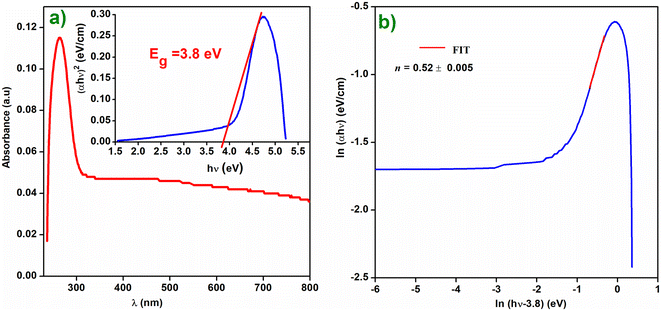 | ||
| Fig. 1 (a) Absorbance spectrum of Cs2ZnCl4. The inset presents the Tauc plot for Cs2ZnCl4, (b) plot of ln(αhν) on y-axis against ln(hν − Eg) on x-axis. | ||
α the optical absorption coefficient is determined using the Beer–Lambert law  . Eg denotes the optical bandgap, n stands for the power factor that displays the transition mode, and β is a constant that illustrates the degree of disorder.
To verify the chosen transition mode, we plotted the variation of ln(αhν) as a function of ln(hν − Eg) as illustrated in Fig. 1(b). The slope of the linear part shown in Fig. 5 shows that the value of n is equal to 0.52, demonstrating the direct mode of transition. Indeed, the power factor represents the transition mode, tending towards two values, 2 or 1/2, depending on whether the forbidden band is indirect or direct and therefore prohibited or authorized. For direct semiconductors (n = 1/2), absorption and emission of photons occur via allowed transitions, but for indirect semiconductors (n = 2), photons and phonons are produced during absorption and recombination. The value of the band gap Eg can be calculated by linear extrapolation to α = 0; Eg is then equal to 3.80 eV. The Cs2ZnCl4 band gap value Eg = 3.8 eV indicates that this material is a semiconductor with a band gap that is appropriate for both visible and near-infrared light emission and absorption.
The empirical link between the absorption coefficient (α) and the energy (hν), which was obtained by the following equation, may be used to determine the disorder in the chemical in accordance with Urbach's law:22
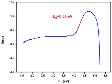
Therefore, using the following equation, we plotted the variation of ln(α) as a function of (hν) in order to determine the value of the Urbach parameter. The EU is inferred from the reciprocal of the linear part slope (Fig. 2). The value of the calculated Urbach energy is EU = 0.55 eV. This value of Urbach energy indicates an intermediate level of disorder or defects in the material. It is higher than the value for CH3NH3SnCl3 (0.25 eV)23 and CsPbBr3 (0.019 eV),24 indicating that Cs2ZnCl4 has a slightly higher disorder. However, it is significantly lower than the value for CH3NH3CdCl3 (1.97 eV),25 implying that Cs2ZnCl4 has better crystalline quality and fewer defects compared to CH3NH3CdCl3.
4.2 Photoluminescence spectroscopy
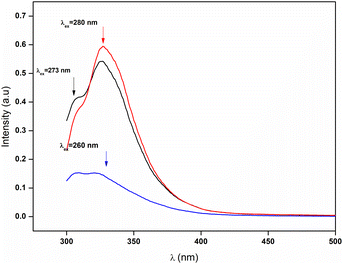
An effective optical method for assessing semiconductor and insulator materials is photoluminescence. The photoluminescence (PL) experiment is used to examine semiconductor compounds in photocatalysis as well as the photochemistry and photo-physics of dielectric materials. Moreover, the PL offers the following details: the isolation and recombination of the photons produced by the load carrier; lattice defects; grain boundaries; and surface oxygen gaps.26Fig. 3 displays the PL spectra of the Cs2ZnCl4 sample at ambient temperature. The photoluminescence spectrum of Cs2ZnCl4 reveals a main emission peak centered around 340 nm, visible for excitation at 260 nm, 273 nm and 280 nm. Among these excitations, the 280 nm one produces the highest intensity, indicating an optimal efficiency to excite the electrons in the material, while the 260 nm excitation shows the lowest intensity, suggesting a lower efficiency. The peak at 340 nm corresponds to near ultraviolet light and results from electronic transitions of electrons from the conduction band to the valence band, emitting light at this specific wavelength when they return to their ground state.27 The wavelength of 340 nm corresponds to 3.65 eV (using the relationship E = hc/λ). This value of Eg agrees well with that found by the absorption data for the UV-visible results (Eg = 3.80 eV). The curves show a rapid rise to the main peak followed by a more gradual decline, which is typical of photoluminescence spectra and reflects a strong and efficient electronic transition. This asymmetrical shape of the curves indicates that the relaxation process of excited electrons is progressive. These observations are essential to understand the optical properties of Cs2ZnCl4 and optimize its use in optoelectronic devices such as UV LEDs and UV sensors.
4.3 Ellipsometry study
The ellipsometry spectroscopy is a technique that accurately determines the optical properties of thin layers by observing the polarization state change of the reflected light. The linearly polarized light beam interacts with the surface, changing from linear to elliptical in polarization. The ellipsometry is an extremely useful tool for determining optical parameters like the refractive index (n) and extinction coefficient (k). Using ellipsometry spectroscopy, the Cs2ZnCl4 sample refractive index was determined.Fig. 4(a) show the variation of the index of refraction (n) as a function of wavelength. It is obvious that the refractive index (n) drops as the wavelength increases, consistent with the Cauchy dispersion relation. This relationship is expressed as:28
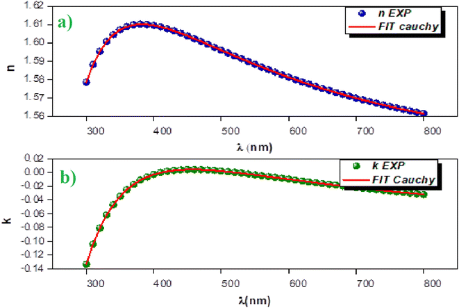 | ||
| Fig. 4 (a) Variation of the refractive index vs. λ, (b) variation of the extinction coefficient vs. λ. | ||
| Cauchy parameters | n0 | k0 | A (μm2) | B (μm4) | C (μm2) | D (μm4) | E0 (eV) | Ed (eV) |
|---|---|---|---|---|---|---|---|---|
| Cs2ZnCl4 | 1.52 | 0.075 | 0.023 | −0.001 | 0.033 | −0.003 | 7.02 | 9.62 |
In addition, the extinction coefficient (k) decreases in the UV region, reaching extremely low levels in the visible spectrum. This behavior suggests that Cs2ZnCl4 may be useful as a UV sensor. The variation of the extinction coefficient (k) as a function of wavelength follows the Cauchy law, expressed as:
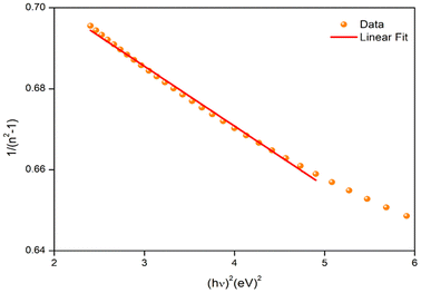
In optical communications and optical device design, the dispersion of a material's refractive index is essential. Therefore, figuring out a material dispersion property is important. A valid oscillator model may be seen in Fig. 5, which displays the variation of refractive index with photons. In order to ascertain the dispersion parameters for the thin film, we employed the Wemple and Di-Domenico model as follows.31
By fitting the linear portion of the curve (n2 − 1)−1 vs. (hν)2, Ed and E0 were calculated from the intercept (E0/Ed) and slope (E0 Ed)−1 on the vertical axis (Fig. 5). The values of E0 and Ed are shown in Table 2. The cohesive energy, or the material's medium bonding force, is connected to the single oscillator energy (E0). The difference between the average energy of atoms in a crystal and the one of free atoms is known as cohesive energy. In addition, it has been empirically estimated that the energy of the oscillator is related to the energy gap by the following relation, E0 = 1.4Eg.32,33 The E0/Eg = 1.4 ratio obtained for Cs2ZnCl4 using the Wemple–Di-Domenico model positions potions this material in an intermediate category compared to other perovskites. For instance, lead-based perovskites like CH3NH3PbI3 typically exhibit a lower ratio, around 1.2 to 1.3, indicating stronger photon–electron interactions and highly favorable optical properties, particularly for solar cell applications. On the other hand, more disordered perovskites, such as CH3NH3CdCl3, show higher E0/Eg ratios, often exceeding 1.6, reflecting a higher defect density and poorer crystalline quality. In comparison, Cs2ZnCl4, with a ratio 1.4, demonstrates a moderate photon–electron interaction while maintaining relatively good crystalline order. This makes it an interesting material, potentially less efficient than lead-based perovskites for applications like solar cells but more stable and less toxic, providing an advantage for optoelectronic applications.
4.4 Confocal microscopy investigation
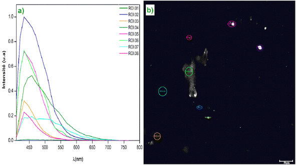
With its rapid scanning capabilities and the ability to define regions of interest (ROIs), the TCS SP8 optimizes imaging while minimizing background noise, enabling the study of the fluorescent characteristics of samples with remarkable precision.The confocal white light microscope often uses many simultaneous rays, allowing for the simultaneous observation of multiple sample locations and the creation of real-time pictures. Confocal microscopy has several benefits over typical optical microscopy, including higher contrast and greater resolution, which enable a thorough examination of the crystals' internal structure.34 The Fig. 6(a) shows a graph of fluorescence spectra (or light intensity) for different regions of interest (ROIs) on the sample taken at a resolution scale of 50 μm. The ROI 01 curve, which has a strong peak at 450 nm, has the best emission efficiency. This may point to an area with the ideal concentration of Cs2ZnCl4 or an area free of large flaws. Different ROIs exhibit different intensities, indicating that fluorescence emission efficiency may vary in different locations. There is a unique electronic transition of Cs2ZnCl4 that is responsible for the primary peak at 450 nm. Multiple electronic transitions may be indicated by the existence of secondary peaks. The Fig. 6(b) shows a map of the analyzed areas of the material Cs2ZnCl4. Fig. 6(b) demonstrate the spatial distribution of optical properties, revealing significant local variations. These observations are important to understand the efficiency of this material in optoelectronic applications.
5 Dielectric properties
The dielectric behavior of materials can be described by the following relationship:| ε(ω) = ε′(ω) + iε′′(ω) | (1) |
 | (2) |
 | (3) |
Fig. 7(a) shows the variation of the real part of the complex dielectric constant as a function of the angular frequency. This variation demonstrates two distinct regions: in the low frequency region, the behavior of the dielectric constant is governed by principal types of polarization: ionic, electronic, interfacial and orientational polarization. The Maxwell–Wagner interfacial polarization theory might explain the variation in the real permittivity component with frequency, in agreement with Koop's phenomenological theory.34 In this model, the material should contain conducting grains separated by poorly conducting grain boundaries.
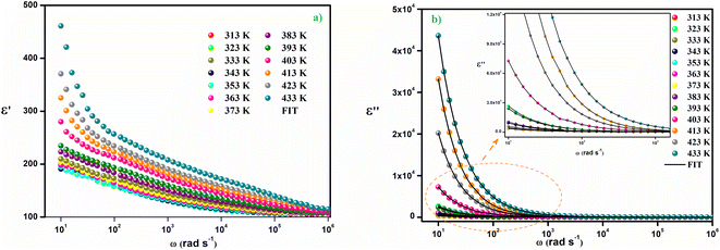 | ||
| Fig. 7 (a) The variation of (ε′) as a function of the angular frequency (ω), (b) the variation of (ε′′) as a function of the angular frequency (ω). | ||
Hence, in order to restrict their flow, charge carriers are effectively trapped at the grain boundary interface.34,35 Electrons exchange between the ions of the same molecules takes place during the polarization process at the interface. The adjustment of the position and distribution of the positive and negative charges of space is caused by the deformations and flaws present in our material. When an electric field is applied, positive and negative charges are affected and move, respectively, towards the applied field's positive and negative poles.36 As a result, a large number of dipoles are formed. In the low frequency domain, electrons can hop to the grain boundary regime, but because of the strong grain boundary resistance, they are collected at the grain boundary position and contribute to polarization. However, as electrons are unable to follow the alternation of the applied field at high frequency, further accumulation of electrons can be prevented even if they have the potential to shift in the other direction. So, the dielectric constant gradually decreases as the frequency rises and as a consequence, electrons have a reduced chance of crossing the grain boundary, which lessens polarization. Therefore, the behavior of the real portion of the electrical response in the region of low frequencies is controlled by orientational and interfacial polarizations which are highly temperature dependent.37 The tendency for ε′(ω) to increase with temperature, as seen in Fig. 7(a), is primarily caused by the presence of load carriers that are activated thermally and the molecular dipole moment.38
The variation of the imaginary part of the dielectric permittivity is plotted on the Fig. 7(b). For this variation, because grain boundaries predominate in the low-frequency region, more energy is needed for electrons to carry out jumps, leading to a high electrical loss (ε′′). In addition, in the high frequency region, the dielectric loss decreases progressively because the exchange of electrons between the ions of the same molecules requires a very small amount of energy. This variation implies that at low frequencies all four types of polarization are present; ionic, electronic, interfacial and orientational polarizations, whereas at high frequencies only ionic and electronic polarizations play a very important role in the reduction of the dielectric loss.37 The dielectric loss tan(δ) as a function of frequency is depicted in Fig. 8(a). Two peaks are noticed on the dielectric loss curve, one at low frequency which corresponds to the space charge effect and the other at high frequency (between 104 and 105 Hz) which is due to the dipolar polarization. The large dielectric permittivity value and low dielectric loss value (between 10−3 and 10) at room temperature of the Cs2ZnCl4 compound imply that this compound has a strong ability to store electrical energy while minimizing energy dissipation as heat. This suggests efficient charge storage with minimal losses, which is advantageous for optoelectronic applications like capacitors or energy storage devices. The low dielectric loss means that the material can retain its electrical energy without significant leakage, making it suitable for applications requiring high energy efficiency. Indeed, materials with a high dielectric constant can be used as a dielectric gate or active channel in FET devices.38,39
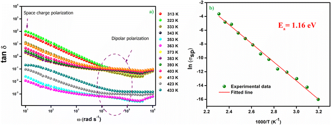 | ||
Fig. 8 (a) Frequency-dependent dielectric loss (tan![[thin space (1/6-em)]](https://www.rsc.org/images/entities/char_2009.gif) δ) of Cs2ZnCl4, (b) variation of ln(σsp) versus 1000/T. δ) of Cs2ZnCl4, (b) variation of ln(σsp) versus 1000/T. | ||
The Cole–Cole modified model with DC conductivity has been used among other popular theoretical models in the goal to study the fluctuation of the dielectric constant and the dielectric loss as a function of frequency at various temperatures.40 According to the modified Cole–Cole model, the complex permittivity may be expressed as follows:
| ε* = ε′(ω) − jε′′(ω) | (4) |
The following equations can also be used to represent the real (ε′) and imaginary (ε′′) parts of the dielectric constant:
 | (5) |
 | (6) |
The Cole–Cole modified equation is used to adjust the experimental data of ε′ and ε′′. The calculated adjustment parameters are listed in Table 2. It is obvious that when the temperature rises, the value of both space charge conductivity (σsp) and free charge conductivity (σfc) increases as demonstrated in Table 2. The value of α is in the range 0.245–0.821. This result further supports the non-Debye nature of the material. The relaxation time decreases when the temperature increases.
The average activation energy of space charge could be determined based on the Arrhenius law as illustrated in the following equation:
The estimated value of the activation energy is 1.16 eV calculated from the slope derivative of the adjustment of ln(σsp) vs. 1000/T (Fig. 8(b)).
6 Analysis of the modulus spectra
In order to get an idea about the relaxation procedure in Cs2ZnCl4, the detailed complex modulus spectra were studied. The complex electrical modulus, in turn, is an extremely easy technique of searching for the electrical relaxation mechanism of the space charge distribution in halting the change generated by the electrodes. This is exactly the reciprocity of the complex permittivity that has been suggested by Macedo. Once the dielectric displacement is continuous, the electric modulus primarily displays the relaxation of the electric field in the material. The formula of the complex modulus is as follows:41–45
 | (7) |
Fig. 9 represents the variation of the real part of the complex modulus (M′) as a function of frequency. The figure demonstrates that for low frequencies M′ is almost zero for all temperatures. This characteristic caused by the elimination of the electrode effects and the charge carriers which are distinguished by their long-distance movement. At higher frequencies M′ decreases as temperature rises, indicating the short-range mobility of the charge carriers inside the Cs2ZnCl4 material.
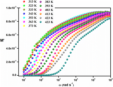 | ||
| Fig. 9 Variation of the real part (M′) of the electrical modulus vs. the frequency at different temperatures. | ||
The variation of the imaginary part of the complex modulus (M′′) as a function of frequency at different temperatures is shown in the Fig. 10(a). M′′ reaches almost zero at low frequencies, demonstrating that the effects of electrode polarization are here negligible. As the frequency is increased, M′′ increases until it reaches an asymptotically maximum value, indicating a relaxation process in Cs2ZnCl4. It is clear that with the increase of temperature, the relaxation peaks are shifted to higher frequencies as a consequence of the temperature dependence of the relaxation mechanism. The asymmetric nature of the peaks demonstrates the non-Debye nature of the material. Besides, the variation of M′′ with frequency is divided into two regions: the left side (i.e., below fmax) is related to long-distance movement of the active charge carrier inside the compound Cs2ZnCl4, while the right side (i.e., above fmax) is related to localized movement. Hence, the peak of relaxation denotes the change of the mobility of the charge carriers from long-distance to short-distance. In order to clarify the asymmetric character of the peaks in the imaginary portion of the modulus, Bergman proposed a general function that considers a modified Kohlrausch–Williams–Watts (KWW) function with two independently defined form parameters for the low frequencies:46–50
 | (8) |
 is the maximum value of the imaginary part of the complex modulus, fmax is the corresponding maximum frequency, a and b are respectively the shape parameters for low and high frequency, c is the smoothing parameter. If a = b = 1 and c = 0 then the eqn (8) is simplified to the eqn (9), which refers to the ideal Debye behavior. The adjustment of the Bergmann function (KWW) is confirmed by the continuous line drawn in the curve (Fig. 10(a)). The values of various parameters are displayed in Table 3. As the temperature rises, the values of the parameters a and b increase, suggesting that M′′(ω) is going to approach the ideal Debye response (Table 4).
 | (9) |
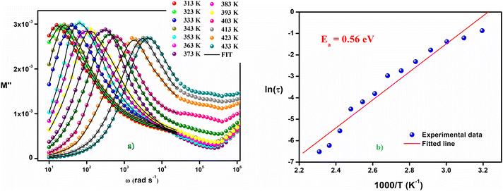 | ||
| Fig. 10 (a) Variation of the imaginary part (M′′) of the electrical modulus vs. the frequency at different temperatures, (b) variation of ln(τ) versus 1000/T. | ||
| Temperature (K) | Parameter | ||||
|---|---|---|---|---|---|
| τ | α | m | σsp | σfc | |
| 313 | 0.41895 | 0.245 | 0.525 | 1.12 × 10⁻⁷ | 5.78 × 10⁻⁶ |
| 323 | 0.29834 | 0.298 | 0.587 | 6.58 × 10⁻⁷ | 9.14 × 10⁻⁶ |
| 333 | 0.2508 | 0.367 | 0.632 | 2.25 × 10⁻⁶ | 3.57 × 10⁻⁵ |
| 343 | 0.16936 | 0.399 | 0.678 | 5.78 × 10⁻⁶ | 8.02 × 10⁻⁵ |
| 353 | 0.09866 | 0.425 | 0.714 | 9.07 × 10⁻⁶ | 9.89 × 10⁻⁵ |
| 363 | 0.06458 | 0.487 | 0.765 | 3.68 × 10⁻⁵ | 2.54 × 10⁻⁴ |
| 373 | 0.05127 | 0.524 | 0.825 | 8.11 × 10⁻⁵ | 6.78 × 10⁻⁴ |
| 383 | 0.02227 | 0.599 | 0.865 | 2.98 × 10⁻⁴ | 1.36 × 10⁻³ |
| 393 | 0.01517 | 0.645 | 0.898 | 7.49 × 10⁻⁴ | 4.74 × 10⁻³ |
| 403 | 0.01081 | 0.677 | 0.914 | 1.66 × 10⁻³ | 8.65 × 10⁻³ |
| 413 | 0.00391 | 0.742 | 0.932 | 5.87 × 10⁻³ | 2.22 × 10⁻² |
| 423 | 0.00198 | 0.784 | 0.945 | 8.08 × 10⁻³ | 5.07 × 10⁻² |
| 433 | 0.00148 | 0.821 | 0.968 | 2.64 × 10⁻² | 8.61 × 10⁻² |
| Temperature (K) | a | b |
|---|---|---|
| 313 | 0.278 | 0.325 |
| 323 | 0.354 | 0.398 |
| 333 | 0.421 | 0.411 |
| 343 | 0.487 | 0.458 |
| 353 | 0.501 | 0.477 |
| 363 | 0.534 | 0.532 |
| 373 | 0.598 | 0.574 |
| 383 | 0.612 | 0.608 |
| 393 | 0.635 | 0.625 |
| 403 | 0.678 | 0.654 |
| 413 | 0.744 | 0.688 |
| 423 | 0.784 | 0.721 |
| 433 | 0.855 | 0.744 |
The following expression was used to calculate the relaxation time:
 | (10) |
The average activation energy of the load carriers can be estimated from the Arrhenius equation;
 | (11) |
These results suggest that Cs2ZnCl4 exhibits thermally activated relaxation behavior. As temperature increases, charge carriers or dipoles become more mobile, allowing for a quicker response to electric fields at higher frequencies. These properties are important for electronic and optoelectronic applications, where the material needs to respond efficiently to varying signals, particularly at different temperatures.
7 Conclusion
In conclusion, the Cs2ZnCl4 sample was obtained using the slow-evaporation technique at ambient temperature. The XRD characterization shows that the elaborate compound belongs to the orthorhombic Pnma space group with the following parameters: a = 9.765(4) Å, b = 7.411(9) Å, c = 12.991(2) Å and V = 940.160(9) Å3. Afterwards, optical analysis demonstrates that the gap and Urbach energy are respectively 3.8 eV and 0.55 eV. The Cs2ZnCl4 photoluminescence spectrum analysis shows that this compound has a main emission peak at 340 nm, with a maximum excitation intensity at 280 nm. These characteristics are crucial to optimize the practical applications of this material in various optoelectronic devices. The refractive index (n) and the extinction coefficient (k) are founds by ellipsometry spectroscopy and obey to the Cauchy law. The refractive index n0 (1.52) and the extinction coefficient K0 (0.075) are lower than those of lead-based perovskite compounds. These adequate results in turn determined the exploitation of these samples in photovoltaic devices. The confocal fluorescence image shows slight variations in intensity which is due to the local inhomogeneity of our sample. The dielectric constant ε′ and the dielectric loss ε′′ increase with temperature and decrease with frequency. Two peaks are noted on the dielectric loss curve, one at low frequency which corresponds to the space charge effect and the other at high frequency which is due to dipolar polarization. The large dielectric permittivity value and low dielectric loss value at room temperature imply that this compound could be a candidate in energy devices. We found that the value of Ea evaluated from the conductivity of the space charge σsp (1.16 eV) is twice the activation energy calculated from the relaxations time (τ). This value confirms that the charge carriers move from long range to short range tunneling. Utilizing its notable optical, electrical, and structural properties, Cs2ZnCl4 shows significant promise for advancing various technological applications. Studies suggest the Cs2ZnCl4 could play a valuable role in fields such as optoelectronics and photovoltaic technologies. For instance, its stability and lower toxicity compared to lead-based perovskites make it an attractive candidate for solar cell applications and other optoelectronic devices.Data availability
All data supporting the findings of this study are included with in the manuscript.Conflicts of interest
The authors declare no conflicts of interest.References
- F. Deschler, M. Price, S. Pathak, L. E. Klintberg, D. D. Jarausch, R. Higler, S. Hüttner, T. Leijtens, S. D. Stranks and H. J. Snaith, et al., J. Phys. Chem. Lett., 2014, 5, 1421 CrossRef CAS.
- Z. K. Tan, R. S. Moghaddam, M. L. Lai, P. Docampo, R. Higler, F. Deschler, M. Price, A. Sadhanala, L. M. Pazos and D. Credgington, et al., Nat. Nanotechnol., 2014, 9, 1 CrossRef.
- K. Xiao, R. Lin, Q. Han, Y. Hou, Z. Qin, H. T. Nguyen, J. Wen, M. Wei, V. Yeddu, M. I. Saidaminov, Y. Gao, X. Luo, Y. Wang, H. Gao, C. Zhang, J. Xu, J. Zhu, E. H. Sargent and H. Tan, Nat. Energy, 2020, 5, 870–880 CrossRef CAS.
- I. L. Braly, D. W. deQilettes, L. M. Pazos-Outon, S. Burke, M. E. Ziffer, D. S. Ginger and H. W. Hillhouse, Nat. Photonics, 2018, 12, 355–361 CrossRef CAS.
- M. M. Lee, J. Teuscher, T. Miyasaka, T. N. Murakami and H. J. Snaith, Science, 2012, 338, 643–647 CrossRef CAS.
- J. H. Noh, S. H. Im, J. H. Heo, T. N. Mandal and S. I. Seok, Nano Lett., 2013, 13, 1764–1769 CrossRef CAS.
- Y.-Y. Zhang, S. Chen, P. Xu, H. Xiang, X.-G. Gong, A. Walshand and S. H. Wei, Chin. Phys. Lett., 2018, 35, 036104 CrossRef.
- S. Chen and G. Shi, Adv. Mater., 2017, 29, 1605448 CrossRef.
- Y. F. Ding, Q. Q. Zhao, Z. L. Yu, Y. Q. Zhao, B. Liu, P. B. He, H. Zhou, K. L. Li, S. F. Yin and M. Q. Cai, J. Mater. Chem. C, 2019, 7, 7433–7441 RSC.
- E. P. Booker, J. T. Griffiths, L. Eyre, C. Ducati, N. C. Greenham and N. J. L. K. Davis, J. Phys. Chem. C, 2019, 123, 16951–16956 CrossRef CAS.
- J. Song, L. Xu, J. Li, J. Xue, Y. Dong, X. Li and H. Zeng, Adv. Mater., 2016, 28, 4861–4869 CrossRef CAS.
- E. Shi, Y. Gao, B. P. Finkenauer, A. Akriti, A. H. Coffey and L. Dou, Chem. Soc. Rev., 2018, 47, 6046–6072 RSC.
- J. He, J. Su, Z. Lin, S. Zhang, Y. Qin, J. Zhang, J. Chang and Y. Hao, J. Phys. Chem. C, 2019, 123, 7158–7165 CrossRef CAS.
- Q. W. Zhou, J. L. Duan, X. Y. Yang, Y. Y. Duan and Q. W. Tang, Angew. Chem., Int. Ed., 2020, 132, 22181–22185 CrossRef.
- J. P. Cao, G. Q. Tang, P. You, T. Y. Wang, F. Y. Zheng, J. Zhao and F. Yan, Adv. Funct. Mater., 2020, 30, 2002358 CrossRef CAS.
- P. Yang, G. Liu, B. Liu, X. Liu, Y. Lou, J. Chen and Y. Zhao, Chem. Commun., 2018, 54(82), 11638–11641 RSC.
- Hybrid bilayer WSe2–CH3NH3PbI3 organo-lead halideas a high performance photodetector.
- S. Hassan, P. Basera, S. Bera, M. Mittal, S. K. Ray, S. Bhattacharya and S. Sapra, ACS Appl. Mater. Interfaces, 2020, 12, 7217–7325 Search PubMed.
- S.-H. Lee, J. Y. Kim, S. Choi, Y. Lee, K. S. Lee, J. Kim and J. Joo, ACS Appl. Mater. Interfaces, 2020, 12, 25159–25167 CrossRef CAS.
- J. A. McGinnety, Inorg. Chem., 1947, 13, 1057–1061 CrossRef.
- Y. Marouani, S. Gharbi, F. Issaoui, E. Dhahri, B. F. O. Costa, M. A. Valente and M. Jemmali, J. Low Temp. Phys., 2020, 200, 131–141 CrossRef CAS.
- S. A. Khan, F. S. Al-Hazmi, S. Al-Heniti, A. S. Faidah and A. A. Al-Ghamdi, Curr. Appl. Phys., 2010, 10, 145–152 CrossRef.
- F. Urbach, Phys. Rev., 1953, 92, 1324 CrossRef CAS.
- S. A. Moyez and S. Roy, J. Nanoparticle Res., 2018, 20, 5 CrossRef.
- Y. Rakita, N. Kedem, S. Gupta and A. Sadhanal, Crystal Growth, ACS Publications, 2016 Search PubMed.
- R. Kalthoum, M. Ben Bechir and A. Ben Rhaiem, Phys. E Low-dimens. Syst. Nanostruct., 2020, 124, 114235 CrossRef CAS.
- K. N. Harish, H. S. B. Naik, P. N. P. Kumar and R. Viswanath, Catal. Sci. Technol., 2012, 2, 1033–1039 RSC.
- S. Kim, B.-K. Yoo, Y. Choi, B.-S. Kim and O.-H. Kwon, Phys. Chem. Chem. Phys., 2018, 20, 11673 RSC.
- A. Jellibi, I. Chaabane and K. Guidara, Phys. E, 2016, 79, 167–172 CrossRef CAS.
- R. K. Singh, R. Kumar, N. Jain, S. R. Dash, J. Singh and A. Srivastava, J. Taiwan Inst. Chem. Eng., 2019, 96, 538–542 CrossRef CAS.
- R. Kalthoum, M. Ben Bechir, A. Ben Rhaiem and M. H. Dhaou, Opt. Mater., 2022, 125, 112084 CrossRef CAS.
- J. H. Joshi, S. Kalainathan, D. K. Kanchan, M. J. Joshi and K. D. Parikh, Arab. J. Chem., 2020, 13, 1532–1550 CrossRef CAS.
- C. He, G. Zha, C. Deng, Y. An and R. Mao, et al., Cryst. Res. Technol., 2019, 54(5), 1900011 CrossRef.
- B. Barış, H. G. Ozdemir, N. Tuğluoğlu, S. Karadeniz and O. F. Yüksel, et al., J. Mater. Sci. Mater. Electron., 2014, 25, 3586–3593 CrossRef.
- K. Alberi, B. Fluegel, H. Moutinho, R. G. Dhere, J. V. Li and A. Mascarenhas, Nat. Commun., 2013, 4, 2699 CrossRef CAS PubMed.
- C. G. Koops, Phys. Rev., 1951, 83, 121 CrossRef CAS.
- M. Ahmad, M. A. Rafiq, K. Rasool, Z. Imran and M. M. Hasan, J. Appl. Phys., 2013, 113, 043704 CrossRef.
- P. Thongbai, S. Tangwancharoen, T. Yamwong and S. Maensiri, J. Phys. Condens. Matter, 2008, 20, 395227 CrossRef.
- S. A. Khan, F. S. Al-Hazmi, S. Al-Heniti, A. S. Faidah and A. A. Al-Ghamdi, Curr. Appl. Phys., 2010, 10, 145 CrossRef.
- M. Gratzel, Nat. Mater., 2014, 13(9), 838–842 CrossRef CAS.
- M. Ben Bechir and A. Ben Rhaiem, J. Solid State Chem., 2021, 296, 122021 CrossRef CAS.
- A. Ajmi, K. Karoui, K. Khirouni and A. Ben Rhaiem, RSC Adv., 2019, 9, 14772 RSC.
- M. Krimi, K. Karoui and A. Ben Rhaiem, J. Alloys Compd., 2017, 698, 510–517 CrossRef CAS.
- N. Mahfoudh, K. Karoui, K. Khirouni and A. Ben Rhaiem, Phys. B, 2019, 554, 126–136 CrossRef CAS.
- M. Ben Bechir, K. Karoui, A. Bulou, M. Tabellout, K. Guidara and A. Ben Rhaiem, J. Appl. Phys., 2014, 116, 214104 CrossRef.
- N. Mahfoudh, K. Karoui and A. Ben Rhaiem, RSC Adv., 2021, 11, 24526–24535 RSC.
- D. K. Rana, S. K. Singh, S. K. Kundu, S. Roy, S. Angappane and S. Basu, New J. Chem., 2019, 43, 3128 RSC.
- S. Patra, P. Sengupta, A. Ray, A. Roy and S. Das, Ceram. Int., 2018, 44, 14236 CrossRef CAS.
- J. Liu, C.-G. Duan, W.-G. Yin, W. N. Mei, R. W. Smith and J. R. Hardy, J. Chem. Phys., 2003, 119, 2812 CrossRef CAS.
- X. Z. Zuo, J. Yang, B. Yuan, D. P. Song, X. W. Tang, K. J. Zhang, X. B. Zhu, W. H. Song, J. M. Dai and Y. P. Sun, J. Appl. Phys., 2015, 117, 114101 CrossRef.
Footnote |
| † Electronic supplementary information (ESI) available. See DOI: https://doi.org/10.1039/d4ra04755a |
| This journal is © The Royal Society of Chemistry 2024 |


