 Open Access Article
Hysteresis in the transfer characteristics of MoS2 field effect transistors: gas, temperature and photo-irradiation effect†
Muhammad Shamim Al Mamun *ad,
Yasuyuki Sainoob,
Tsuyoshi Takaoka
 b,
Atsushi Andoc and
Tadahiro Komeda
 b
b
aDepartment of Chemistry, Graduate School of Science, Tohoku University, Aramaki-Aza-Aoba, Aoba-Ku, Sendai 9808578, Japan. E-mail: s.mamun@chem.ku.ac.bd
bInstitute of Multidisciplinary Research for Advanced Materials (IMRAM, Tagen), Tohoku University, 2-1-1, Katahira, Aoba-Ku, Sendai 9800877, Japan
cNational Institute of Advanced Industrial Science and Technology, 1-1-1 Umezono, Tsukuba, Ibaraki 305-8568, Japan
dChemistry Discipline, Khulna University, Khulna, 9208, Bangladesh
First published on 15th November 2024
Abstract
We report the characteristic behaviors of the hysteresis observed in the transfer characteristics of back-gated field-effect transistors with an exfoliated MoS2 channel under various conditions. We find that the hysteresis is strongly enhanced by temperature, environmental gas, or light irradiation. Our measurements reveal the characteristic hysteresis behaviors in a 1 atm oxygen environment, which we explain as an oxygen molecule facilitated charge acceptor on the MoS2 surface. The decrease in the current value in the ON state of the device may indicate that oxygen molecules are more effective charge acceptors than nitrogen molecules. We conclude that intrinsic defects in MoS2, such as S vacancies, which result in effective adsorbate trapping, play an important role in the hysteresis behavior, in addition to oxygen and nitrogen adsorbates on the passivated device surface. The availability of thermally or photo-generated minority carriers (holes) in MoS2 is increased by both light and temperature. This leads to subsequent processes of positive charge trapping, which intensify the hysteresis.
Introduction
Molybdenum disulfide (MoS2) has received much attention as the most popular semiconductor from the family of transition metal dichalcogenides.1 The bulk form of MoS2 is composed of stacks of two-dimensional layers that are weakly constrained by van der Waals interactions. Each MoS2 layer is formed by three atomic planes, with the Mo plane sandwiched between two S planes. Since the interlayer bonds are weak, it is possible to obtain monolayer MoS2 using scotch tape or liquid phase exfoliation, similarly to graphene.2–5 Chemical vapor deposition (CVD) from heated S and MoO3 powders has become the standard fabrication method for large-scale production.6 Bulk MoS2 has an indirect band gap of 1.2 eV, while monolayer MoS2 has a direct band gap of 1.8 eV.7,8 This large bandgap, combined with mechanical flexibility, makes MoS2 suitable as a channel for field-effect transistors (FETs) for logic applications.Hysteresis features appear as two well-separated current levels, especially when gases are stably adsorbed on the channel, and can be exploited in memory devices. Chalcogen vacancies favor natural n-type doping in MoS2 and act as trap centers that enhance the hysteretic behavior in MoS2 and other 2D TMDs.9–11
Initial studies of the photo-response of TMD films were carried out at room temperature and in air. At this stage, no claims were made about the decay time of the photocurrent. The rise and decay in the time-resolved photocurrent after switching on and off 532 nm laser illumination under various conditions revealed that adsorbent impurities are an important player in determining the time decay of photocurrents after irradiation with light.12 Furthermore, even if a pure (pristine) MoS2 surface was prepared, time decay of the photocurrent was observed. More recently, researchers have focused on the trap states caused by defects or residual impurities at MoS2/SiO2 interfaces. However, the effect of environmental gas conditions, temperature and light irradiation on the photo-response of MoS2 devices is still unclear.
In this paper, we fabricate back-gated, exfoliated-MoS2 transistors and investigate the effects of environmental conditions, temperatures and light irradiation on the hysteresis behavior. Our study confirms that hysteresis is enhanced by oxygen molecules adsorbed on the device surface and can be quenched by reducing the pressure or the temperature. Our experimental findings suggest that hysteresis is strongly related to oxygen adsorption on the gate channel, which facilitates charge transfer and trapping, and is favored when thermally generated or photogenerated minority carriers (holes) become available in the n-type MoS2 transistor. We suggest that intrinsic defects such as S vacancies or other interfacial states, which result in effective positive charge trapping, are an important cause of hysteresis.
Experimental
We started by ultrasonicating a wafer (300 nm SiO2 on p++Si substrate) in the solvents acetone and isopropanol for five minutes each. A thicker SiO2 layer may lower the leakage currents and hysteresis, but can also have an impact on the overall device performance by slowing the switching speed and raising series resistance. On the other hand, while thinner SiO2 layers provide greater electrostatic control, they are more vulnerable to leakage problems and hysteresis.13 Thus, optimization of the dielectric thickness is important. In our previous studies, 300 nm SiO2 was used successfully.14–16 The substrate was further cleaned using a 30 min UV-O3 treatment after being dried using a N2 gas flow. The MoS2 flake was transferred to SiO2 on a Si substrate using the mechanical exfoliation technique with scotch tape.17–19 In short, a piece of 3 cm scotch tape was cut, and a small amount of bulk MoS2 was placed on the tape. Next, using two hands, the scotch tape was twisted so that the separated MoS2 flakes covered nearly the entire surface of the scotch tape. Then, the MoS2 flakes were placed on the p++Si substrate by simply flipping the scotch tape. The thickness of the MoS2 layer was estimated (i) by measuring the contrast of the reflected light from the SiO2 surface with and without the MoS2 flakes,20 (ii) using Raman spectroscopy21 and (iii) using atomic force microscopy (AFM).22 The contrast was defined using the following equation:where R0(λ) and R(λ) are the intensities of the reflected light without and with MoS2 for the wavelength λ, respectively. It has been suggested that the use of λ in the red region is more efficient compared to the use of blue and green lights.3
MMA (methyl methacrylate) and PMMA (poly(methyl methacrylate)) resists were applied on the flake. Electrode patterning was conducted using electron beam lithography (ELS-700, ELIONIX). Following development, an electron-beam evaporator was used to form the source and drain contacts of Ti (10 nm)/Au (150 nm). Ultimately, N-methyl-2-pyrrolidone (NMP) was used in a wet removal procedure to carry out the lift-off operation. A wire bonding machine (7476D, WEST-BOND) was used to wire the produced device on a Cu-epoxy circuit board using Al wire (0.05 mm, 1% Si/Al). The MoS2-FET device's FET characteristics were assessed using an external source measure unit (SMU 2634, Keithley), to which SMA cables were used to link both the device and the electric feedthrough that was connected to the UHV chamber. Two rotary pumps and one ion pump were used to maintain a high vacuum of 10−6 Pa. External gas cylinders were used to pass the oxygen and nitrogen gas into the chamber. A depiction of the UHV chamber and gas transfer process is shown in Fig. S2.†
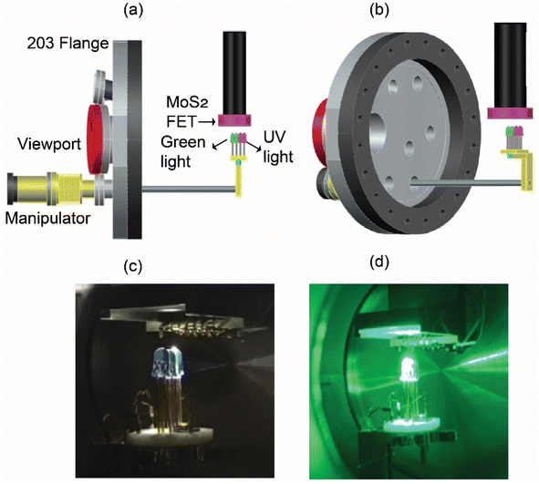
The electrodes for the source and the drain were formed by depositing Ti layers followed by Au layers. The device was mounted under a continuous flow cryostat LT3B Helitran® (ADVANCED RESEARCH SYSTEMS) in the vacuum chamber. Two LED arrays faced to the device surface were mounted on the linear motion feedthrough as displayed in Fig. 1 (a) side view and (b) angle view, which were attached inside the vacuum chamber and used as the light sources, as shown in Fig. 1 (c) for UV light and (d) for green light. The distance between the LED and MoS2 device was set to around 5 mm. The wavelengths of the LEDs were 365 and 525 nm. The transfer and output characteristics of the devices were measured using a Keithley 2634B source measure unit. The signal coaxial cables were connected via electrical feedthrough to the measurement system.
Results and discussion
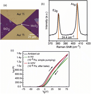
Fig. 2(a) shows an optical image of the back-gated FET device with four layers of MoS2 flakes. The channel length and width of the sample are L = 3.0 μm and W = 3.9 μm, respectively. The C(λ) of the red light was found to be 0.58, which indicated the number of the layers of the flakes to be four.3 The Raman spectrum of the MoS2 flakes was also obtained to determine the flake thickness, and is displayed in Fig. 2(b). The separation of 24.4 cm−1 between the two characteristic peaks (A1g and E2g) indicated four-layer MoS2 flakes. AFM also confirmed that the MoS2 flake thickness is about four layers (2.9 nm), as shown in Fig. S3.† Fig. 2(c) shows the transfer characteristics (Ids–Vg curves, where Ids is the drain-source current and Vg is the gate voltage) under ambient air, high vacuum (HV; 10−5 Pa) and ultra-high vacuum (UHV; 10−6 Pa). The HV condition was achieved by simple evacuation of air using a turbo-molecular pump for several hours, and UHV was achieved by baking the vacuum chamber (device temperature kept at ∼330 K) for 46 h followed by cooldown to room temperature for 14 h. We note that the on-state current at VG = 80 V was increased by heating the device. The device exhibits n-type behavior, similar to previous reports.23–26With lowering the pressure, the hysteresis was suppressed effectively. The decrement in the hysteresis with lowering the pressure indicates that the hysteresis is mainly attributed to the adsorbed molecules in air that act as charge-trapping centers. The transfer curves in different Vg sweep directions would be considerably affected by the trapped charges due to adsorbates on the device channel. This indicates that the hole (electron) trap is responsible for the negative (positive) shift of the transfer curve in the forward (backward) sweep direction, and the time constant for charge trapping/de-trapping is comparable to the measurement time with 5 V s−1 as shown in the present study. These results are highly consistent with various previous reports.27–32
After the device heating, on-state current at VG = 80 V was improved ∼15%. Although residual gas, especially H2O, should be removed, a small hysteresis still remained. This result indicates an intrinsic origin of hysteresis in the MoS2 device, which was attributed to the presence of defects and point vacancies in the MoS2 or charge traps at the interface.33
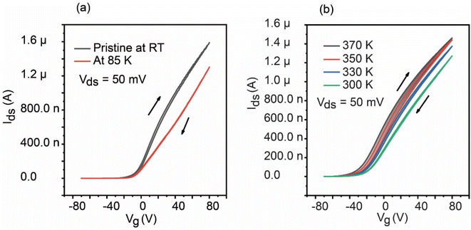
The intrinsic charge trapping effect in MoS2 has a strong temperature dependance and should be suppressed by cooling down the device. We observed a temperature effect in the hysteresis, as shown in Fig. 3. The hysteresis was drastically reduced when the device was cooled below room temperature to around 85 K, as shown in Fig. 3(a). Furthermore, the linearity of the transfer characteristics was improved at low temperature. These results indicate that the hysteresis ascribed to the charge trapping was almost suppressed at 85 K. The device was heated to around 370 K at 10−5 Pa overnight to ensure the removal of H2O and impurities. After baking, we measured the transfer characteristics during the cooldown to room temperature, as shown in Fig. 3(b). While wider hysteresis was observed at higher temperature, the hysteresis decrease depended on the temperature during cooldown. A similar temperature dependence was observed for the other devices we fabricated. The disappearance of the hysteresis at low temperatures is attributed to the prolonged time constant for charge trapping/de-trapping.12,27 Thus, cooling the device in an easily attainable temperature range is one way to suppress the hysteresis or instability without surface passivation, which could be highly advantageous for the device applications of this system.
It is well known that water molecules strongly influence the magnitude of the hysteresis under ambient conditions.34 We focused on the main components of the atmosphere other than water, namely, oxygen and nitrogen molecules, and studied the characteristics that appeared in the hysteresis. The device was heated to around 100 °C at 10−5 Pa overnight in both cases to ensure the removal of H2O and impurities in the same manner as for Fig. 3. After cooling to room temperature, the pressure was recovered to 10−6 Pa. Following that procedure, the environmental dry gas was introduced into the UHV chamber via a variable leak valve. The purity of the environmental dry gas was 99.7% for oxygen and 99.999% for nitrogen. The pressure was controlled using a variable leak valve and measured with a B-A gauge over the range of 10−6 to 101 Pa and a Bourdon gauge for −0.1 to +0.11 MPa. The measurement was carried out just after achieving the target pressure, and the environmental gas was kept flowing.
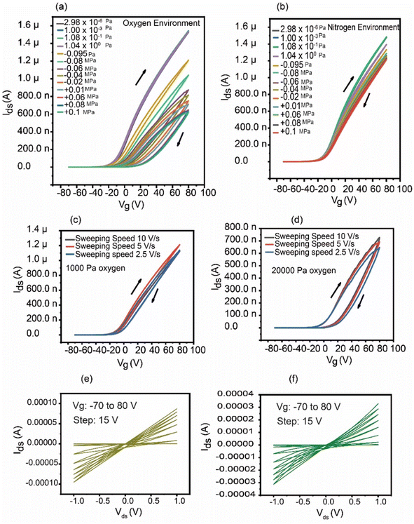
Fig. 4 shows the transfer characteristics in the different environmental gases (a) oxygen and (b) nitrogen. The oxygen environment led to remarkably increased hysteresis due to the gas dosing, while nitrogen resulted in small changes in the hysteresis. We note that the device showed similar Ids–Vg curves (black line) before introducing the environmental gas; furthermore, the maximum Ids at the highest Vg was decreased compared with that observed in the UHV environment in both the oxygen and nitrogen environment cases. The percentage reduction in the on-state current, i.e., the Ids at Vg = 80 V, was ∼63% for the 1 atm oxygen environment and ∼20% for 1 atm nitrogen, respectively. Oxygen has an acceptor nature and traps electrons on this surface. We observed interesting behavior in the hysteresis in tests of the gas pressure effect and photo-response in an oxygen environment. Sulfur-vacancies, namely, chalcogen vacancies, favor natural n-type doping in MoS2 and act as trap centers that enhance the hysteretic behavior in MoS2 and other 2D TMDs.28 Our results indicate that the oxygen molecule is greatly preferred to adsorb to and interact with chalcogen vacancies over nitrogen. In principle, these defects should influence the surface adsorption, which in turn can passivate these donors, affecting both the concentration and the mobility of the carriers in the layer. Based on DFT calculations, the S-vacancy acts as a donor state that lies approximately 0.25–0.5 eV below the conduction-band minimum and gives rise to several new energy states in the forbidden gap.34,35 Since oxygen has a great effect on hysteresis, the effect of the voltage sweep rate was examined at two different oxygen pressures. Fig. 4(c) and (d) depict the effects of different voltage sweep rates (2.5, 5, and 10 V s−1) on hysteresis at two distinct oxygen pressures, 1000 Pa and 20![[thin space (1/6-em)]](https://www.rsc.org/images/entities/char_2009.gif) 000 Pa, respectively. In both instances, it is observed that the hysteresis decreases at the fastest sweep speed. This is because MoS2 FETs typically have lower hysteresis, since it takes less time for the charge trapping and de-trapping processes to take place. This results in steadier transfer characteristics over the voltage sweep range since the device has less time to interact with charge traps.36 Fig. 4(e) and (f) demonstrate the output characteristics (Ids–Vds) of the device with a pristine surface and after oxygen injection (1.0 × 10⁻³ Pa), respectively. After oxygen was introduced at a pressure of 1.0 × 10⁻³ Pa, the device output characteristics showed very slight changes in the hysteresis curves, but the drain current decreased as linearity was lost. This suggests that when the amount of carrier trapping/scattering centers increases slightly, there is a small decrease in electron injection from the Au/Ti contacts into MoS2. This behavior is similar to the transfer characteristics measured in Fig. 4(a), which shows that no visible changes were observed in the hysteresis curves after the introduction of oxygen at 1.0 × 10⁻³ Pa. We hypothesized that if the output characteristics were measured at a higher oxygen dose, a clear change in the hysteresis curve would be observed. Linear growth of Ids with Vds indicates good ohmic contact between the electrodes and MoS2 at the pristine surface.37 Following the introduction of oxygen, Ids dropped and deviated from linearity at increasing Vg, particularly in the positive voltage range, which may be because of the adsorption of oxygen at the vacant sites of MoS2, where it acts as an electron acceptor. The voltage sweep direction was reversed (80 V to −70 V) to investigate whether any changes in the duration of the charge trapping/de-trapping process would occur, as displayed in Fig. S4.† However, no significant change was observed. Peize Han et al. described the mechanism of the origin of hysteresis induced by oxygen and water molecules under ambient conditions.38 The mechanism for the origin of hysteresis in the presence of only oxygen is shown in Fig. 5 in a similar manner.
000 Pa, respectively. In both instances, it is observed that the hysteresis decreases at the fastest sweep speed. This is because MoS2 FETs typically have lower hysteresis, since it takes less time for the charge trapping and de-trapping processes to take place. This results in steadier transfer characteristics over the voltage sweep range since the device has less time to interact with charge traps.36 Fig. 4(e) and (f) demonstrate the output characteristics (Ids–Vds) of the device with a pristine surface and after oxygen injection (1.0 × 10⁻³ Pa), respectively. After oxygen was introduced at a pressure of 1.0 × 10⁻³ Pa, the device output characteristics showed very slight changes in the hysteresis curves, but the drain current decreased as linearity was lost. This suggests that when the amount of carrier trapping/scattering centers increases slightly, there is a small decrease in electron injection from the Au/Ti contacts into MoS2. This behavior is similar to the transfer characteristics measured in Fig. 4(a), which shows that no visible changes were observed in the hysteresis curves after the introduction of oxygen at 1.0 × 10⁻³ Pa. We hypothesized that if the output characteristics were measured at a higher oxygen dose, a clear change in the hysteresis curve would be observed. Linear growth of Ids with Vds indicates good ohmic contact between the electrodes and MoS2 at the pristine surface.37 Following the introduction of oxygen, Ids dropped and deviated from linearity at increasing Vg, particularly in the positive voltage range, which may be because of the adsorption of oxygen at the vacant sites of MoS2, where it acts as an electron acceptor. The voltage sweep direction was reversed (80 V to −70 V) to investigate whether any changes in the duration of the charge trapping/de-trapping process would occur, as displayed in Fig. S4.† However, no significant change was observed. Peize Han et al. described the mechanism of the origin of hysteresis induced by oxygen and water molecules under ambient conditions.38 The mechanism for the origin of hysteresis in the presence of only oxygen is shown in Fig. 5 in a similar manner.
 | ||
| Fig. 5 Illustration of charge transfer between the adsorbed O2 molecules and MoS2. (a) Vg = −80 V and (c) Vg = 70 V in the Ids–Vg plot (b). | ||
The adsorption of molecules at these vacancy sites passivates the donors, resulting in a reduction in the electron concentration in the conduction band, as shown in Fig. 5(a). Since it is highly electronegative, oxygen has an acceptor nature and traps electrons from MoS2. When a positive voltage is applied to the gate channel, as shown in Fig. 5(c) to the right of the hysteresis displayed in Fig. 5(b), the MoS2 surface becomes electron-rich. Electrons fill the charge traps, rendering them neutral and leading to a positive VTH shift. The electrons remain trapped until the reverse sweep, during which they are de-trapped.39 Oxygen molecules easily adsorb on the surface by accepting electrons from the surface (O2 + e− → O2−). Due to the decrease in electron density for molecule adsorption, the on-state current decreases and Vth shifts to positive. At a negative gate voltage, the MoS2 channel becomes filled with holes and the adsorbed molecules return electrons to surface (O2− + h → O2),32,40 while molecule desorption happens as shown in Fig. 5(a) to the left.38 Therefore, at negative gate voltages, the concentration of adsorbed molecules and electron-filled traps (along with their hole-doping effect) is suppressed, and the threshold shifts towards negative gate voltages. Theoretically, DFT calculations predict that the physisorption of O2 molecules on MoS2 occurs with a binding energy of 79 meV, and that approximately 0.04 electrons per O2 are transferred to the molecules.41
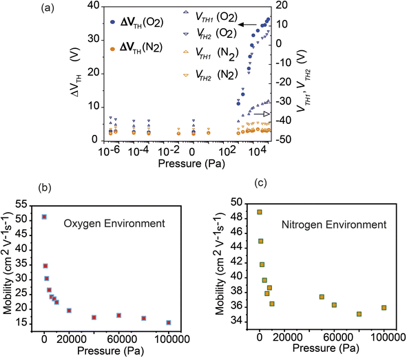
To clarify the charge trapping effect due to the environmental gas, we plotted the differential threshold voltage (ΔVTH) versus gas pressure as shown in Fig. 6(a). The method of calculation for the threshold voltage is shown in the SI. The differential threshold voltages ΔVTH = VTH2 − VTH1 in different sweep directions, where VTH1 is for the forward (off–on direction) sweep and VTH2 for the backward (on–off) sweep, are defined as the voltages at which the drain–source current is Ids = 1 nA. The ΔVTH value indicates the separation degree of the hysteresis. In both the oxygen and nitrogen gas introduction conditions, VTH1 and VTH2 were shifted in the positive direction. In an oxygen environment, VTH1 shifted much more than VTH2, and as a result, a large hysteresis appeared. The separation of the hysteresis curve increased rapidly from an oxygen partial pressure of about 1000 Pa, and ΔVTH exceeded 36 V at 1 atm. While the hysteresis in the nitrogen environment did not show such a clear difference compared to that observed for oxygen, it did exhibit a slight increase in the hysteresis compared with that observed under UHV, and the difference in the threshold voltage depending on the sweep direction widened to about 3.2 V at 1 atm. The mobility of the device following oxygen input is shown in Fig. 6(b). The device's mobility dropped significantly under these conditions from around 52 to 15 cm2 V−1 s−1, while in the case of nitrogen, it dropped from approximately 49 to 36 cm2 V−1 s−1, as shown in Fig. 6(c). This phenomenon shows that, in comparison to nitrogen, oxygen has a more significant impact on the device performance, leading to greater hysteresis.
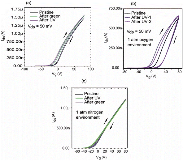
Considering the applications of MoS2-based FETs to optical functions, it is particularly important to investigate the change in the transfer curve due to light irradiation under various environmental (gas) conditions. In general, the photo-response of the MoS2-FET device is determined using the Id variation under UV and green light irradiation, as shown in Fig. 7(a). The Id variation is also helpful to understand photo-switching, persistent photoconductivity, and the relaxation of photocurrent, etc. In this work, we focused on the changes in the hysteresis of the Ids–VG curve due to light irradiation in the vacuum and gas environments. The light irradiation effect on the Ids–Vds curves in oxygen and nitrogen environments is shown in Fig. 7(b) and (c), respectively. The light irradiation was carried out using an LED array mounted inside the chamber. The wavelengths of the LEDs were 365 nm (UV) and 525 nm (visible green). The driving current for the LEDs was If = 26 mA. The Ids–VG measurements were performed just after light irradiation in the dark. The on-state current for Ids at VG = 80 V was increased after light irradiation. When the MoS2-FET device in the vacuum and nitrogen environment was irradiated with light, both the threshold voltage VTH1 (forward) and VTH2 (backward) shifted in the negative direction, and as a result, we obtained almost the same ΔVTH. Interestingly, in the case of the device in an oxygen environment, the light irradiation caused the threshold voltage of VTH1 to shift appreciably in the negative direction, while VTH2 was pinned to almost the same value, and the on–off (backward) curve kept almost the same shape. The differential threshold ΔVTH became 10 times larger than that before light irradiation. The light irradiation seems to result in modification of the band structure of MoS2, as shown in Fig. 7(a) in the case of UHV. Basically, photo-irradiation activates the trap state intermediate band gap and produces photoconductivity. While the UHV and nitrogen environment results show a similar response to the light irradiation, characteristic features were observed in the oxygen environment. Light substantially increases the channel conductance for photoconductive and photogating effects9,42 Both temperature and light increase the availability of thermally or photo-generated minority carriers (holes) in MoS2 and enable additional processes of positive charge trapping, which further enhance the hysteresis. During the forward VG sweep, adsorbed oxygen molecules easily desorb from the surface supported by the light excitation and hole-producing effect, while O2 desorption in the backward VG sweep might be suppressed due to reduced hole-creation effect. The reason for the trapping on-to-off curve in Id–VG after light irradiation in oxygen environment seems to be complicated. Further study is required to identify the origin of the photo-response in detail, e.g., other gas adsorbates on the device channel and/or chemical impurities between the SiO2 interface.
We also investigated the recovery process. In the case of light irradiation in an oxygen or nitrogen environment at 1 atm, the Ids curve returned to almost its original state after the device was left in the dark for several days, with some dependence on the time of light irradiation. In contrast, the effect of light irradiation on MoS2-FET in an ultra-high vacuum seemed to persist for an exceedingly long time. The hysteresis curve did not return to its original state over after 100 h. Again, heating the device under vacuum was effective to nearly recover the device to its pristine state under vacuum.
A comparison table is given in Table 1 regarding the main factors responsible for the device hysteresis. From the table, it is clear that oxygen is the main factor in the hysteresis in the field effect transistor devices, which is consistent with our findings.
| Thickness of SiO2 | Number of layers of MoS2 | Hysteresis conditions | References |
|---|---|---|---|
| 270 nm | Bulk layer | Oxygen, nitrogen, and air and nitrogen with varying relative humidities | 27 |
| — | CVD-grown monolayer | Oxygen, nitrogen, hydrogen and methane | 28 |
| 300 nm | Monolayer | Humidity and illumination | 29 |
| 300 nm | Monolayer | MoS2 itself | 33 |
| 285 nm | Monolayer | Water and oxygen | 34 |
| 300 nm | Four layers | Oxygen, nitrogen, temperature, UV, and green light | Present work |
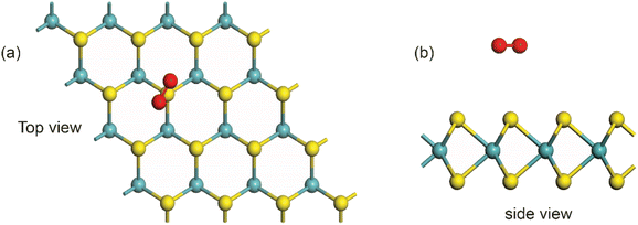
To investigate the electron transfer process, the interaction between an MoS2 slab and an oxygen molecule was investigated via density functional theory (DFT). The optimized model of MoS2 with oxygen is shown in Fig. 8 in (a) top view and (b) side view. All DFT calculations were performed using the Vienna ab initio simulation package (VASP)43 with the generalized gradient approximation (GGA) – Perdew–Burke–Ernzerhof (PBE) functionality. The energy cutoff of the plane-wave basis was set to 400 eV. For energy minimization, the convergence threshold was set at 10−5 eV, while for force, it was set at 0.01 eV Å−1. For the structural relaxation, the Brillouin zone was represented using a 3 × 3 × 1 Monkhorst–Pack k-point mesh, and for the self-consistent computations, a 10 × 10 × 1 mesh. To prevent interactions between monolayer MoS2, the 4 × 4 × 1 MoS2 slab in the supercell was vacuum-sealed at a thickness of 15 Å. Grimme's expression implemented the vdW correction for physical adsorption configurations.44 A significant amount of oxygen is analytically physisorbed onto the MoS2 FET when oxygen is injected into the vacuum chamber. Bader analysis indicates that the physisorbed oxygen molecules are electron donors and cause p-type doping. Our theoretical models closely align with earlier atomic-scale reports.45 Bader analysis shows that about 1.06 e− is transferred per molecule from MoS2 to oxygen molecule.
In terms of data reproducibility, two different MoS2-FET devices were used under the same oxygen exposure conditions, as shown in Fig. S5.† It is clearly seen that effect of oxygen on the hysteresis behavior of the two devices is almost the same. We believe that this is possible due to the benefit of using an ultra-high vacuum chamber.
Conclusion
We have described the distinctive hysteresis behavior in the transfer characteristics seen under different circumstances for back-gated field-effect transistors with an exfoliated MoS2 channel. We have discovered that changes in temperature, ambient gas, or light irradiation all significantly increase hysteresis. The hysteresis in a 1 atm oxygen environment exhibits distinctive behavior, which we attribute to the oxygen molecule acting as a charge acceptor on the MoS2 surface. It is possible that oxygen molecules are a better charge acceptor than nitrogen molecules based on the decrease in the device current value when it is in the ON state. We infer that, in addition to oxygen and nitrogen adsorbates on the passivated device surface, intrinsic defects in MoS2, such as S vacancies, which lead to effective adsorbate trapping, are crucial in the hysteresis behavior. Both temperature and light increase the amount of thermally or photogenerated minority carriers (holes) in MoS2. This causes further positive charge trapping processes, which amplify the hysteresis.Data availability
Any kind of data will be supplied if requested.Author contributions
Muhammad Shamim Al Mamun: writing – original draft, visualization, methodology, investigation, conceptualization. Yasuyuki Sainoo: writing – original draft, visualization, methodology, investigation, conceptualization. Tsuyoshi Takaoka: writing – review & editing, investigation. Atsushi Ando: writing – review & editing. Tadahiro Komeda: writing – review & editing, project administration, funding acquisition.Conflicts of interest
There are no conflicts to declare.Acknowledgements
This study was supported in part by Grant-in-Aid for Scientific Research (S) (No. 19H05621) (for TK), and by ‘‘Nanotechnology Platform Program’’, grant number JPMXP09F20C023.References
- Z. Lin, A. McCreary, N. Briggs, S. Subramanian, K. Zhang, Y. Sun, X. Li, N. J. Borys, H. Yuan, S. K. Fullerton-Shirey, A. Chernikov, H. Zhao, S. McDonnell, A. M. Lindenberg, K. Xiao, B. J. LeRoy, M. Drndić, J. C. M. Hwang, J. Park, M. Chhowalla, R. E. Schaak, A. Javey, M. C. Hersam, J. Robinson and M. Terrones, 2D Materials, 2016, 3, 042001 CrossRef
.
- A. Di Bartolomeo, Phys. Rep., 2016, 606, 1–58 CrossRef CAS
.
- N. T. Trung, M. I. Hossain, M. I. Alam, A. Ando, O. Kitakami, N. Kikuchi, T. Takaoka, Y. Sainoo, R. Arafune and T. Komeda, ACS Omega, 2020, 5, 28108–28115 CrossRef CAS
.
- M. S. A. Mamun, H. Waizumi, T. Takaoka, M. I. Alam, Y. Tanaka, A. Ando, Z. Wang and T. Komeda, Nanotechnology, 2021, 32, 075501 CrossRef PubMed
.
- H. Waizumi, M. Shamim Al Mamun, T. Takaoka, M. Iftekharul Alam, Y. Tanaka, A. Ando, Z. Wang, R. Arafune and T. Komeda, Appl. Surf. Sci., 2022, 571, 151252 CrossRef CAS
.
- X. Li and H. Zhu, J. Materiomics, 2015, 1, 33–44 CrossRef
.
- J. K. Ellis, M. J. Lucero and G. E. Scuseria, Appl. Phys. Lett., 2011, 99, 261908 CrossRef
.
- K. F. Mak, C. Lee, J. Hone, J. Shan and T. F. Heinz, Phys. Rev. Lett., 2010, 105, 136805 CrossRef PubMed
.
- A. Di Bartolomeo, L. Genovese, T. Foller, F. Giubileo, G. Luongo, L. Croin, S. J. Liang, L. K. Ang and M. Schleberger, Nanotechnology, 2017, 28, 214002 CrossRef PubMed
.
- A. Di Bartolomeo, A. Pelella, X. Liu, F. Miao, M. Passacantando, F. Giubileo, A. Grillo, L. Iemmo, F. Urban and S.-J. Liang, Adv. Funct. Mater., 2019, 29, 1902483 CrossRef
.
- M.-L. Tsai, S.-H. Su, J.-K. Chang, D.-S. Tsai, C.-H. Chen, C.-I. Wu, L.-J. Li, L.-J. Chen and J.-H. He, ACS Nano, 2014, 8, 8317–8322 CrossRef CAS
.
- W. Zhang, J.-K. Huang, C.-H. Chen, Y.-H. Chang, Y.-J. Cheng and L.-J. Li, Adv. Mater., 2013, 25, 3456–3461 CrossRef CAS
.
- J. H. Sim, S. C. Song, P. D. Kirsch, C. D. Young, R. Choi, D. L. Kwong, B. H. Lee and G. Bersuker, Microelectron. Eng., 2005, 80, 218–221 CrossRef CAS
.
- M. S. A. Mamun, Y. Sainoo, T. Takaoka, H. Waizumi, Z. Wang, M. I. Alam, A. Ando, R. Arafune and T. Komeda, Phys. Chem. Chem. Phys., 2021, 23, 27273–27281 RSC
.
- M. S. Al Mamun, H. Waizumi, T. Takaoka, Z. Wang, A. Ando and T. Komeda, Org. Electron., 2024, 126, 106989 CrossRef CAS
.
- M. S. A. Mamun, Y. Tanaka, H. Waizumi, T. Takaoka, Z. Wang, M. I. Alam, A. Ando, M. Fukuyama, A. Hibara and T. Komeda, Phys. Chem. Chem. Phys., 2020, 22, 27724–27731 RSC
.
- K. S. Novoselov, D. Jiang, F. Schedin, T. J. Booth, V. V. Khotkevich, S. V. Morozov and A. K. Geim, Proc. Natl. Acad. Sci. U. S. A., 2005, 102, 10451–10453 CrossRef CAS
.
- K. S. Novoselov, A. K. Geim, S. V. Morozov, D. Jiang, M. I. Katsnelson, I. V. Grigorieva, S. V. Dubonos and A. A. Firsov, Nature, 2005, 438, 197–200 CrossRef CAS PubMed
.
- K. S. Novoselov, A. K. Geim, S. V. Morozov, D. Jiang, Y. Zhang, S. V. Dubonos, I. V. Grigorieva and A. A. Firsov, Science, 2004, 306, 666–669 CrossRef CAS PubMed
.
- Y. Y. Wang, R. X. Gao, Z. H. Ni, H. He, S. P. Guo, H. P. Yang, C. X. Cong and T. Yu, Nanotechnology, 2012, 23, 495713 CrossRef PubMed
.
- H. Li, Q. Zhang, C. C. R. Yap, B. K. Tay, T. H. T. Edwin, A. Olivier and D. Baillargeat, Adv. Funct. Mater., 2012, 22, 1385–1390 CrossRef CAS
.
- M. Tosun, D. Fu, S. B. Desai, C. Ko, J. Seuk Kang, D.-H. Lien, M. Najmzadeh, S. Tongay, J. Wu and A. Javey, Sci. Rep., 2015, 5, 10990 CrossRef PubMed
.
- M. Egginger, S. Bauer, R. Schwödiauer, H. Neugebauer and N. S. Sariciftci, Monatsh. Chem., 2009, 140, 735–750 CrossRef CAS
.
- H. Li, Z. Yin, Q. He, H. Li, X. Huang, G. Lu, D. W. H. Fam, A. I. Y. Tok, Q. Zhang and H. Zhang, Small, 2012, 8, 63–67 CrossRef CAS PubMed
.
- M. Fontana, T. Deppe, A. K. Boyd, M. Rinzan, A. Y. Liu, M. Paranjape and P. Barbara, Sci. Rep., 2013, 3, 1634 CrossRef PubMed
.
- M. Gobbi, S. Bonacchi, J. X. Lian, A. Vercouter, S. Bertolazzi, B. Zyska, M. Timpel, R. Tatti, Y. Olivier, S. Hecht, M. V. Nardi, D. Beljonne, E. Orgiu and P. Samorì, Nat. Commun., 2018, 9, 2661 CrossRef PubMed
.
- Y. Shimazu, M. Tashiro, S. Sonobe and M. Takahashi, Sci. Rep., 2016, 6, 30084 CrossRef CAS PubMed
.
- F. Urban, F. Giubileo, A. Grillo, L. Iemmo, G. Luongo, M. Passacantando, T. Foller, L. Madauß, E. Pollmann, M. P. Geller, D. Oing, M. Schleberger and A. Di Bartolomeo, 2D Materials, 2019, 6, 045049 CrossRef CAS
.
- D. J. Late, B. Liu, H. S. S. R. Matte, V. P. Dravid and C. N. R. Rao, ACS Nano, 2012, 6, 5635–5641 CrossRef CAS
.
- H. Qiu, L. Pan, Z. Yao, J. Li, Y. Shi and X. Wang, Appl. Phys. Lett., 2012, 100, 123104 CrossRef
.
- T. Li, G. Du, B. Zhang and Z. Zeng, Appl. Phys. Lett., 2014, 105, 093107 CrossRef
.
- K. Cho, W. Park, J. Park, H. Jeong, J. Jang, T.-Y. Kim, W.-K. Hong, S. Hong and T. Lee, ACS Nano, 2013, 7, 7751–7758 CrossRef CAS
.
- J. Shu, G. Wu, Y. Guo, B. Liu, X. Wei and Q. Chen, Nanoscale, 2016, 8, 3049–3056 RSC
.
- A. Di Bartolomeo, L. Genovese, F. Giubileo, L. Iemmo, G. Luongo, T. Foller and M. Schleberger, 2D Materials, 2018, 5, 015014 CrossRef
.
- S. Deb, P. Bhattacharyya, P. Chakrabarti, H. Chakraborti, K. Das Gupta, A. Shukla and S. Dhar, Phys. Rev. Appl., 2020, 14, 034030 CrossRef CAS
.
- C. Li, C. Wen, R. Zeng, S. Zeng, Z. J. Qiu, Z. Zhang, S. L. Zhang and D. Wu, IEEE Electron Device Lett., 2020, 41, 1356–1359 CAS
.
- J. Shan, J. Li, X. Chu, M. Xu, F. Jin, X. Wang, L. Ma, X. Fang, Z. Wei and X. Wang, RSC Adv., 2018, 8, 7942–7948 RSC
.
- P. Han, E. R. Adler, Y. Liu, L. St Marie, A. El Fatimy, S. Melis, E. Van Keuren and P. Barbara, Nanotechnology, 2019, 30, 284004 CrossRef CAS PubMed
.
- I. M. Datye, A. J. Gabourie, C. D. English, K. K. H. Smithe, C. J. McClellan, N. C. Wang and E. Pop, 2D Materials, 2019, 6, 011004 CrossRef CAS
.
- J. Pak, M. Min, K. Cho, D.-H. Lien, G. H. Ahn, J. Jang, D. Yoo, S. Chung, A. Javey and T. Lee, Appl. Phys. Lett., 2016, 109, 183502 CrossRef
.
- S. Tongay, J. Zhou, C. Ataca, J. Liu, J. S. Kang, T. S. Matthews, L. You, J. Li, J. C. Grossman and J. Wu, Nano Lett., 2013, 13, 2831–2836 CrossRef CAS PubMed
.
- M. K. Ghimire, H. Ji, H. Z. Gul, H. Yi, J. Jiang and S. C. Lim, ACS Appl. Mater. Interfaces, 2019, 11, 10068–10073 CrossRef CAS PubMed
.
- J. Hafner, J. Comput. Chem., 2008, 29, 2044–2078 CrossRef CAS
.
- S. Grimme, J. Antony, S. Ehrlich and H. Krieg, J. Chem. Phys., 2010, 132, 154104 CrossRef PubMed
.
- G. Sun, F. Li, T. Wu, L. Cong, L. Sun, G. Yang, H. Xie, A. Mauger, C. M. Julien and J. Liu, Inorg. Chem., 2019, 58, 2169–2176 CrossRef CAS PubMed
.
Footnote |
| † Electronic supplementary information (ESI) available. See DOI: https://doi.org/10.1039/d4ra04820b |
| This journal is © The Royal Society of Chemistry 2024 |


