DOI:
10.1039/D4RA05001K
(Paper)
RSC Adv., 2024,
14, 27332-27342
First-principles study of electronic, optical, and thermoelectric properties of KMCuS3 (M = Th and Sm) quaternary chalcogenides†
Received
11th July 2024
, Accepted 23rd August 2024
First published on 28th August 2024
Abstract
Copper-based quaternary chalcogenides are considered as intriguing material systems in terms of their remarkable optoelectronic and thermoelectric properties. Here we investigated the light interaction and electronic transport properties of novel KMCuS3 (M = Th, Sm) materials. Advanced computations based on density functional theory were used for these calculations. The PBE-GGA scheme predicted band gaps for the KSmCuS3 and KmThCuS3 were 0.61, and 2.03 eV, respectively. While the TB-mBJ computed band gap values for KSmCuS3 and KThCuS3 were 0.91, and 2.39 eV, respectively. A direct band gap nature for both materials was confirmed by identifying the CBM and VBM at the same high symmetry gamma point. The Cu-d, Sm-f, Th-f, and S-p orbitals unified to form the valence band region at the BZ high symmetry point, while the Th-d and Sm-d orbitals formed the conduction band region. Furthermore, linear optical properties such as complex dielectric function components, along with other important optical parameters were computed and explained for possible employment in optoelectronic devices. The considerable thermoelectric characteristics were also predicted, and the incredible outcomes were described, implying that these compounds have potential for thermoelectric applications.
1. Introduction
Quaternary chalcogenides have recently attracted a lot of attention due to their potential uses in diverse areas, including electronics, optoelectronics, energy conversion or storage, and thermoelectric applications.1–3 Most of these compounds are predominantly composed of rare earth and chalcogen elements, with interesting features that make them promising candidates for cutting-edge technological applications.4–6 Among the group of these quaternary chalcogenides, the copper-based quaternary compounds are particularly attractive.7–10 The interaction of potassium (K), copper (Cu), sulfur (S), and other rare earth species (M) produces a wide range of physical and chemical phenomena that require further exploration. The optoelectronic characteristics of these quaternary materials are vital for their optoelectronic applications such as sensors, light-emitting devices, and photovoltaics.11–15 Understanding the band structures, energy levels, and charge transport processes of copper-based quaternary chalcogenides is also significant for the full employment of their potential usage in different applications.16–18 Additionally, some research on the thermoelectric feature of these materials has grown in importance in the hunt for long-term energy solutions. The use of these quaternary materials with excellent thermoelectric properties to convert waste heat into useable power can improve energy efficiency. To acquire high efficiency from any solar cell, the optical band gap of semiconductors used in various photovoltaic cell manufacturing must match the solar spectra having a high mobility, optical band gap, and high absorption coefficient.19–22 It is common knowledge that the optical band gap of semiconductors made of these quaternary chalcogenides fits the solar spectrum. The characteristics above amply demonstrate the suitability of the nonlinear optical Li2In2SiS6 crystal for building a non-linear optical component. On the other hand, Li2In2XY6 (X = Ge, Si and Y = S, Se) systems with four diverse iso-structures were created by Yin et al.,23 and their research indicated that these materials were crystallized in a CC space group with a monoclinic phase.
The Li2In2SiS6, Li2In2SiSe6, Li2In2GeSe6, and Li2In2GeS6 had calculated energy gap values of 3.24, 2.35, 1.92, and 2.99 eV, respectively, according to Kin Mun Wong et al.24 The predicted energy gap values by employing diffuse-reflectance spectra, were comparable with the experimental energy gap values. The Li2In2SiY6 (Y = S, Se) with computed energy gap values that are bigger than those of the Li2In2GeY6 (Y = S, Se). It also suggests that Li2In2SiY6 (Y = S, Se) materials could accomplish an improved role once selected as novel IR non-linear optical systems.25 According to Muhammad Abubakr et al.26 the projected band gaps of some studied quaternary compounds drop in the order SrCu2GeS4 (0.696 eV), BaCu2GeS4 (0.668 eV), BaCu2GeSe4 (0.379 eV), and SrCu2GeSe4 (0.195 eV). This decrease in energy bandgaps demonstrates the substantial impact that different dopants have on the electronic and optical features for the XCu2GeM4 (X = Sr, Ba and M = S, Se). To determine their potential for optoelectronic applications, these materials' optical properties were examined. Additionally, these quaternary chalcogenides are also potential thermoelectric materials based on predicted thermoelectric characteristics. The SrCu2GeSe4 (2.6), BaCu2GeSe4 (1.85), SrCu2GeS4 (1.01), and BaCu2GeSe4 (0.94) were the ZT values of studied quaternary XCu2GeM4 (X = Ba, Sr, and M = S, Se) systems.26 In particular, the Cu2Se4 tetrahedral array functions as an electrically conducting ingredient in the quaternary Cu2CdSnSe4 selenide, whereas the CdSnSe4 array functions as an insulating constituent.27 The Cu2CdDIVQ4 type chalcogenides also exhibit large Seebeck coefficients in addition to having low thermal conductivity.28 The predicted energy gap values of 0.96 eV for Cu2CdSnSe4,27 1.19–1.20 eV for Cu2CdGeSe4,29 1.14–1.52 eV for Cu2CdSnS4,30–34 and 1.85 eV for Cu2CdGeS4,35 the compounds are observed to be semiconductors. Numerous physicochemical characteristics of these quaternary chalcogenides can be controlled and altered to meet desired technical requirements for such solid solution production. By adjusting the S/Se ratio, it is possible to obtain tunable band gaps in Cu2CdSn (S, Se)4 solid solutions ranging from 0.94 to 1.4 eV.36
Tombak et al.,37 studied the Cu2HgSnSe4 crystal structure and predicted with a = 5.8288 Å and c = 11.4179 Å. Hirai et al.,38 first examined the phase diagram for HgSe–Cu2SnSe3 system, where the Cu2HgSnSe4 molecule occurs. They found that there is a solid solution between Cu2HgSnSe4 and Cu2SnSe3, as well as a significant interaction between the quaternary selenide and HgSe. They also found that alloying the Cu2HgSnSe4 compound boosted thermal conductivity; however, the thermoelectric figures of merit ZT were not improved in this situation. The Cu2HgSnSe4 combination crystallizes uniformly, and its melting points, which were determined based on several investigations of the HgSe–Cu2SnSe3 phase diagram, were 710 °C,38 697 °C,39 and 708 °C.40 A quaternary system such as Cu2HgSnSe4 has a positive thermoelectric power, and its Seebeck coefficient can reach up to 1.7 × 10³ V K−1, showing a p-type semiconducting nature.38 Its figure of merit is of the order of 10−4 °C−1 that was far lower than those found for other comparable quaternary selenides, like Cu2ZnSnSe4 (up to 0.45)41 and Cu2CdSnSe4 (up to 0.7).42 Similarly, the Cu2HgSnSe4 nanocrystals with regulated composition were produced by Li et al.,43 using a synthetic method. These nanocrystals had relatively low electrical conductivity and a Seebeck coefficient that was higher than that of ref. 38 but less than that concluded by Li et al.43 However, in this situation, the partial replacement of the mercury and copper atoms permitted a rise in the electrical conductivity.43 In this work, we investigated in detail the optoelectronics and thermoelectric properties of the novel KMCuS3 (M = Th, and Sm) quaternary chalcogenides using state-of-the-art DFT calculations. We shed light on these materials' electronic band structures, density of states, optical absorption spectra, and thermoelectric transport coefficients. We have fresh perspectives from our computational study that could guide the practical synthesis and characterization of this work, paving the way for the development of novel optoelectronic and thermoelectric applications.
2. Computational method
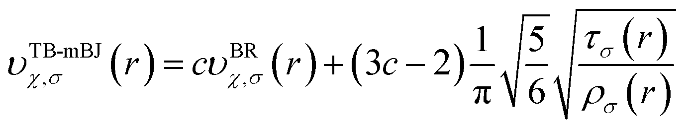
The full-potential linearized augmented plane wave (FP-LAPW) method as employed in Wien2k package that employs a was used to carry out the first-principles calculations. The Becke-Johnson potential44 was used to improve the energy band gap and is given by the expression as:| |
 | (1) |
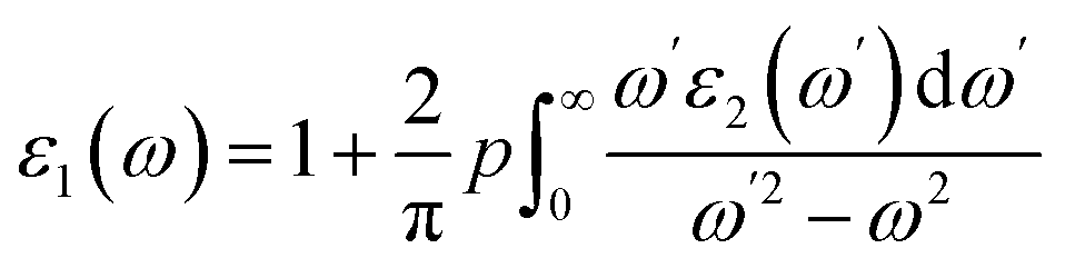
The GGA functional, such as PBE, considers both the electron density at a location and its gradient.45 When analyzing insulators or semiconductors, traditional DFT techniques like PBE-GGA frequently undervalue band gaps.45 The band gap prediction can be improved by the mBJ exchange–correlation potential, which introduces a twist to the functional exchange portion. The exchange and correlation effects are modeled with the Tran Balaha modified Becke-Johnson exchange potential (TB-mBJ) and the generalized gradient approximation proposed by Perdew, Burke, and Ernzerhof (PBE-GGA). For optimization, lattice parameters and atomic positions were relaxed. The system size contained a unit cell with 24 atoms with the unit cell of KThCuS3 composed of four K atoms, four Th atoms, four Cu atoms, and twelve S atoms, all arranged in an orthorhombic crystal system and has computed lattice vectors of a = 4.45 Å, b = 6.74 Å, and c = 11.15 Å, respectively. Similarly, the unit cell of KSmCuS3 composed of four K atoms, four Sm atoms, four Cu atoms, and twelve S atoms, all arranged in an orthorhombic crystal system and has computed lattice vectors of a = 4.42 Å, b = 6.66 Å, and c = 11.02 Å respectively. Furthermore, the muffin-tin radii (RMT) have been chosen correctly for each atom type to avoid overlap and maximize computing efficiency. The values of the muffin radii are 2.01 for K, 2.51 for Th, 2.31 for Sm, 2.0 for Cu, and 1.7 bohr for S, are selected. Using a dense (10 × 10 × 10) k-point grid in the first BZ reciprocal space, we carried out these calculations. When the force convergence threshold reaches roughly 10−4 eV Å−1 the iterations are stopped, and the self-consistent criterion is chosen to have an accuracy of 10−6 Ry. The sum of the smallest atomic spheres radii (Rmin) and the prime reciprocal vector modulus (Kmax) was taken to equal 8. It is decided that −6.0 Ry will serve as the cut-off energy for defining the separation of core-valence states. Lmax = 8 and Gmax = 14 were selected as the additional input for the Wien2k package. The Fourier-expanded charge density is shown by Gmax, and lmax was the highest value of the angular momentum vector. The complex dielectric function two components were computed in the present optical properties study and as expressed as:46
| |
 | (2) |
| |
 | (3) |
The other significant optical parameters were also computed from the ε1(ω), and ε2(ω) expressions:46
| |
 | (4) |
| |
 | (5) |
| |
 | (6) |
| |
 | (7) |
| |
 | (8) |
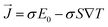
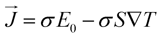
The BoltzTrap code47 is used for the important thermoelectric features in the present calculations. The stiff band approximation was employed as in generalized semi-classical BoltzTrap scheme to consider the intricate estimations for these thermoelectric characteristics. The relaxation period was considered as energy-independent in many cases, and in the present case it was set at 8.02 × 10⁻¹⁵ seconds. These vital thermoelectric properties are primarily computed using the Boltzmann Transport Theory and the Onsager's relations as given:47
| |
 | (9) |
| |
 | (10) |
Here the
σ, ∇
T,
S,
E0, and

are the electric conductivity, the temperature gradients, Seebeck coefficient, external electric field, and the electrical current density, respectively.
3. Results and discussion
3.1 Electronic band structures
KThCuS3 crystallizes in the orthorhombic with the space group Cmcm, as shown in Fig. 1.
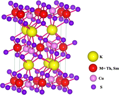 |
| | Fig. 1 The crystal structure for KMCuS3 (M = Th, Sm) materials with Vesta package. | |
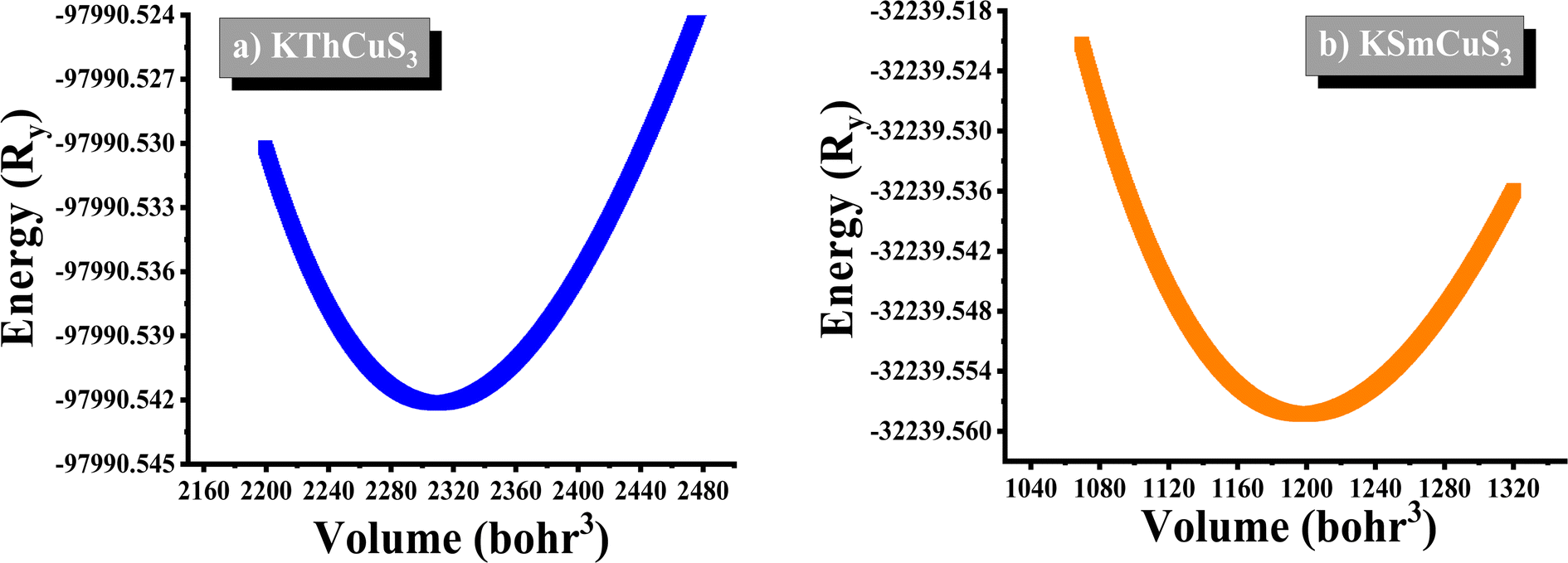
The K1+ atom is bound to eight S2− atoms in an 8-coordinate geometry. The K–S bond distances range from 3.18 to 3.65 Å. Th4+ is bound to six S2− atoms, forming ThS6 octahedra. These are divided into two ThS6 octahedra, two ThS6 octahedra, and four CuS4 tetrahedra. There are four short (2.69 Å) and two long (2.78 Å) Th–S bonds. Cu1+ binds to four S2− atoms, forming CuS4 tetrahedra. These are divided into four equivalent ThS6 octahedra and two equivalent CuS4 tetrahedra. There are two lengths of Cu–S bonds (2.29 Å and 2.44 Å, respectively). KSmCuS3 also crystalizes the orthorhombic with the Cmcm group of crystals. K1+ has an 8-coordinate geometry and is linked to eight S2− atoms. The K–S bond distances range from 3.15 to 3.65 Å. Th4+ is bound to six S2− atoms, forming SmS6 octahedra. These divide corners into two SmS6 octahedra, two SmS6 octahedra, and four CuS4 tetrahedra. There are four short (2.68 Å) and two long (2.76 Å) Sm–S bond lengths. Cu1+ is bound to four S2− atoms, forming CuS4 tetrahedra. These are divided into two appropriate CuS4 tetrahedra and four equivalent ThS6 octahedra. There are two Cu–S bond lengths: short (2.27 Å) and long (2.39 Å). Understanding a material's energy band structure may help determine how useful it could be in creating efficient electronic devices. These electronic structures are closely related to the crystallographic structures of the materials. An object's energy gap and electronic configuration have a direct or indirect impact on its physical features. The narrow band gap semiconductors usually could be desirable for thermoelectric applications, whereas optoelectronic applications typically focus on the direct band gap characteristic of a semiconductor together with its width. These structures stability was confirmed by their predicted formation energy values. The computed formation energy values for the KSmCuS3 and KmThCuS3 quaternary system were −1.93 and 1.98(eV per f.u.) respectively. Using the Birch–Murnaghan equation of state, the total energy KSmCuS3 and KmThCuS3 is minimized regarding variations in the unit cell volume shown in Fig. 2. This allows for the identification of the ideal ground state parameters. Near the equilibrium volume (V0), the system is stable in equilibrium. Increasing the volume significantly from V0 results in a decrease in energy since the system is transitioning to a more stable state. As the material approaches equilibrium, its potential energy decreases and its volume expands somewhat. At the equilibrium volume, the energy reaches its lowest point (E0). This is the most stable arrangement for the material. As the volume exceeds the equilibrium volume, the energy begins to grow again. This is because the material is being stretched beyond its stable structure, increasing potential energy owing to increasing atomic distance.
 |
| | Fig. 2 The energy vs. volume optimization curves for (a) KThCuS3 (b) KSmCuS3 quaternary materials. | |
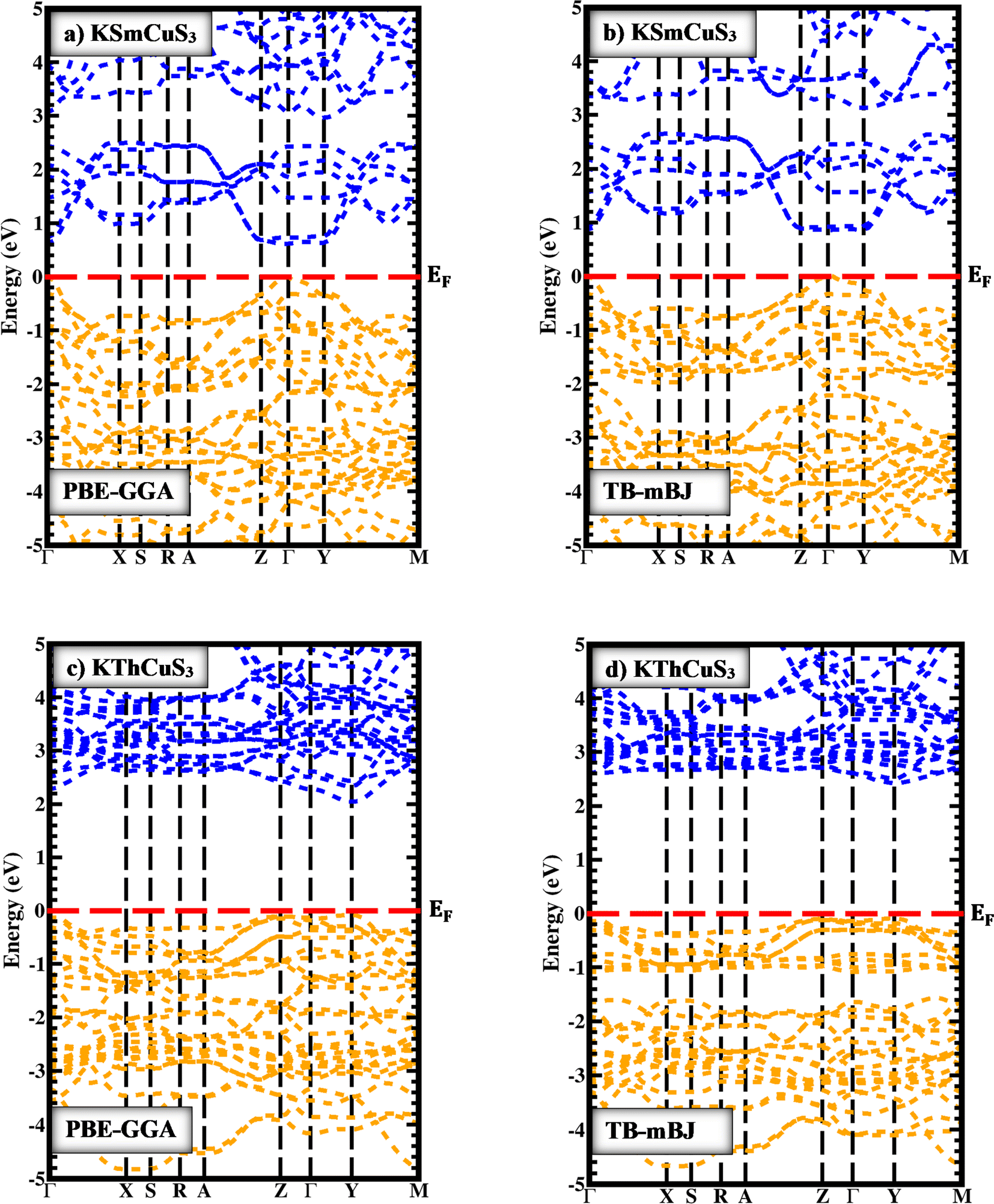
In Fig. 3(a and c) the PBE-GGA was used to predict the band profiles with high-symmetry points within the first BZ of the KSmCuS3 quaternary system. The conduction band minima and valence band maxima are located at the gamma (Γ) symmetry point for both these systems. Both compounds exhibit direct band gap behavior. The Fig. 3(b and d) using TB-mBJ, also confirmed the direct band gap nature for both compounds. By employing PBE-GGA scheme, the predicted energy gap values for KSmCuS3 and KmThCuS3 are 0.61, and 2.03 eV, respectively. Whereas the TB-mBJ results for KSmCuS3 and KThCuS3 are 0.91, and 2.39 eV, respectively. The electronic band gap energy was enhanced by higher coulomb repulsion between CB and VB that is brought about by the TB-mBJ approximation. These KMCuS3 (M = Sm, Th) semiconductors possess a narrow bandgap. The estimated band profiles for KSmCuS3 are shown in Fig. 3(a and b). At the BZ (Γ) point, the Cu-d, and S-p states combine to form the valence band. At the BZ (Γ) point, the Sm-d state shaped the conduction band at its maximal location. The predicted band profiles of KThCuS3 were illustrated in Fig. 3(c and d). At the BZ (Γ) point, the conduction band maximum location is formed by the Th-d state. In optoelectronic devices, the direct band gap characteristics of these semiconductors are of utmost significance. The initial approximations used were PBE-GGA, but most focus was given to the predicted results from the TB-mBJ because this approach can correct accurately the band splitting, leading to improved band gaps and an enhanced optical transition between the valence and conduction bands. This crystal structure and atomic configuration of a materials unit cell have a direct impact on the material's electronic band structure. Variations in energy band dispersion and bandgap values can be caused by the particular arrangement of atoms and their interactions. When compared to KThCuS3, the bandgap of KSmCuS3 might be smaller if the atoms are positioned in a way that promotes better electron contacts or energy level overlap. In the electronic structures, the localized Sm-d and Th-f orbitals are introduced by the presence of rare earth and transition metal (Cu) ions. These orbitals have the potential to interact with one another as well as with the orbitals of other atoms, causing changes in the bandgap and energy band positions. Various materials can have distinct orbital energy and interactions.
 |
| | Fig. 3 The band profiles with PBE-GGA and TB-mBJ for (a and b) KSmCuS3 (c and d) KThCuS3 quaternary materials. | |
3.2 Density of states
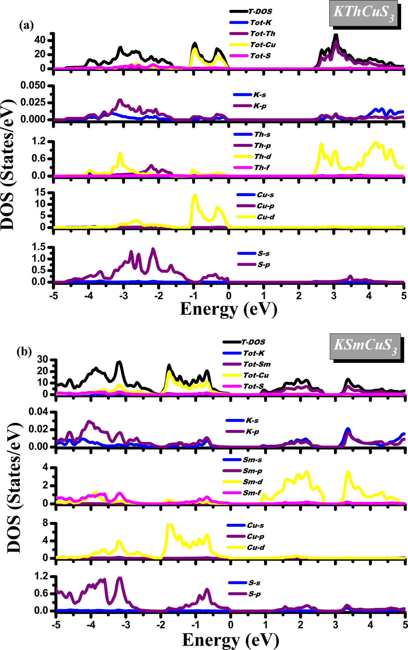
Most of the physical characteristics, including the measurement of dielectric functions, transport features, material photoemission spectra, etc., depend on the density of states (DOS). Diverse energy states with an influence on the VB and CB are also explained by their corresponding density of states. These compounds display a semiconducting nature from their DOS calculations as the Fermi level splits these VB and CB. Fig. 4(a and b) shows the calculated density of state plots for these quaternary materials. In a range of −0.8 up to −2.0 eV, the TDOS plot in the VB band is observed for KSmCuS3 compounds. The Tot-Cu states contribute significantly to this form VB band. In the VB, discrete peaks from −0.8 to 5.0 eV are observed in PDOS plots. The hybridization of the K-s/p, Sm-d/f, Cu-d, and S-p states created this region. The Cu-d and S-p states contributions in the valence band between −0.5 and 2.0 eV energy range are the source of the first observed peak. Due to the contributions of the Sm-f states, there are additional minor peaks noticed in this energy range. Similarly, to that, the Cu-d, K-s, and Sm-d/f states each contribute a negligible amount in the energy range. The Tot-Sm states are the dominant contributor in the TDOS plot in the conduction band region. The Sm-d states influence the most to PDOS plots in the conduction band region from 0.9 eV up to 2.4 eV, followed by K-p and S-p states with smaller contributions. Similar to the first zone in CB, the second region from 3.3 eV to 5.0 eV has a significant contribution from Sm-d states and k-s/p states. In the 0.0 up to −1.2 eV range, which corresponds to the prominent peaks from the Tot-Cu states. The Cu-d states are responsible for the majority of the peaks in PDOS plots in the VB, with small contributions from K-p and S-p states, and these peaks occur in the 0.0 up to −1.2 eV range. From S-p states, and Th-d states in the VB from −1.2 to around 3.5 eV energy range, the second region peak appears. The K-s and Th-p states make up a relatively modest portion of this energy range.
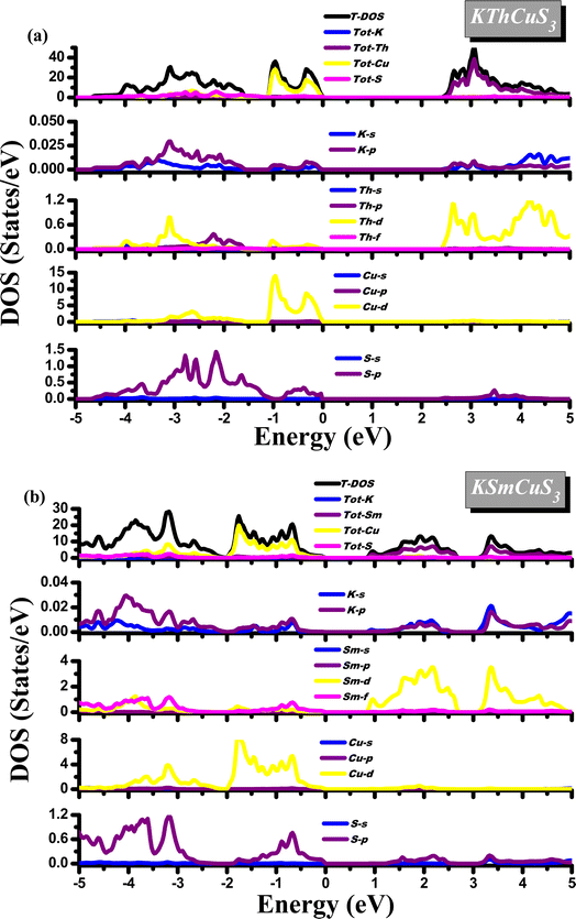 |
| | Fig. 4 The calculated density of states for (a) KThCuS3 (b) KSmCuS3 quaternary materials. | |
In the CB, according to the TDOS, the Tot-Th states contribute mostly from 2.5 eV to 5.0 eV. In PDOS graphs in the CB, the Th-d state contributes the most and the K-s/p state contributes the least in the range of 2.5 up to 5.0 eV. Different atomic orbitals (Cu-d, and S-p) and interactions between these atoms are responsible for the various peaks in the DOS of the valence band region of both KSmCuS3 and KThCuS3 systems. In its outermost electron shell, potassium (K), an alkali metal, normally possesses just one valence electron. In the p orbital sits the valence electron for potassium. When potassium interacts electronically with other elements to generate compounds like KSmCuS3, overlapping atomic orbitals can result in the formation of these energy bands. Because valence electrons in these bands come from the potassium p orbitals, they can contribute most to DOS peaks in the valence band region. The transition metal copper (Cu) is also distinguished by its partially filled d orbitals. Due to interactions with nearby atoms and the effects of crystal fields, the d orbitals in compounds can split into different energy bands. The DOS peaks in the valence band region can be attributed to the partially filled d orbitals of copper. These peaks may be the result of different interactions and hybridizations between d orbitals and other orbitals, which produce energy levels within the valence band. The nonmetal sulfur (S) has valence electrons arranged in the p orbital. Energy bands formed by p orbital overlap can be produced by interactions between sulfur and other atoms in the complex, just like in the case of potassium. The valence band region's DOS peaks may be influenced by valence electrons coming from sulfur's p orbitals.
3.3 Optical properties
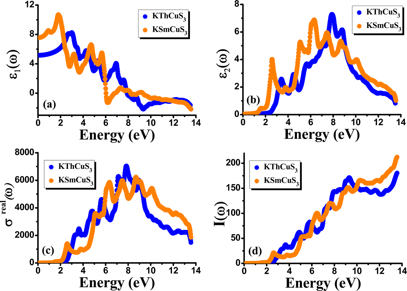
The complex dielectric function, which is defined by the equation ε(ω) = ε1(ω) + iε2(ω) displays the response of the optical nature of a material at all photon energies. The dielectric function's real part ε1(ω) which depicts energy held in a material. In contrast, the second term denotes the imaginary component ε2(ω) that is associated with the materials' absorption characteristics as well as the compound's electronic band structure. Fig. 5(a) depicts how the complex dielectric function of the KMCuS3 (M = Th, and Sm) compounds vary as photon energy increases. The values of ε1(0) for KThCuS3 and KSmCuS3 are 5.5 and 7.5, respectively, at low frequency (ω = 0). For the KThCuS3 and KSmCuS3 materials, the maximum values of ε1(ω) are 8.5 and 10.5 eV respectively, and peaks in ε1(ω) spectra exist. Additionally, for the compounds KThCuS3 and KSmCuS3, the ε1(ω) are negative in the energy range of 7.5–11.5 eV and 5.5–7.2 eV, respectively. Thus, for these photon energy range, the materials exhibit metallic behaviour and turn reflective in the direction of the incoming photons. The threshold energy of the ε2(ω) for the KThCuS3 and KSmCuS3 compounds are 2.4 eV and 1.2 eV, respectively, as shown in Fig. 5(b), which also shows the fluctuation of the absorptive part of the dielectric function. For each compound above this threshold energy, magnitude of the ε2(ω) rise along the energy. In addition, the cause of the observed various peaks in the ε2(ω) may be connected to these PDOS for KMCuS3 (M = Th, and Sm) quaternary compounds.
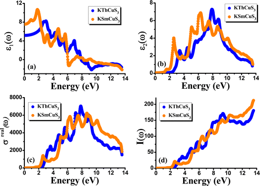 |
| | Fig. 5 The calculated (a) real component (b) imaginary component (c) real part of optical conductivity (d) absorption coefficient for KMCuS3 (M = Th, and Sm) materials. | |
These variations in peak height are important because they result from electronic interband transitions as observed in the ε2(ω). For KThCuS3 and KSmCuS3, the principal peak, which denotes the largest of energy transitions, corresponds to energy values of 3.1, 5.0, and 7.5 eV and 2.5, 5.5, and 6.5 eV, respectively. The energy bands in the material may begin to converge at greater photon energies. This may result in a reduction in the density of transition-ready energy levels, a reduction in absorption, and a corresponding reduction in the ε2(ω). From the incident electromagnetic radiation, a material's optical conductivity explains how it reacts, notably in terms of absorbing and reemitting light. The imaginary part of optical conductivity is related to the damping or dissipation of those excitations, whereas the real part is connected to the absorption of light and the excitation of charge carriers. The frequency dependent optical conductivity for the KMCuS3 (M = Th, and Sm) compounds varies with energy, as seen in Fig. 5(c). It is evident that the optical conductivity threshold energies for the compounds KThCuS3 and KSmCuS3 are 2.5 eV and 2.3 eV, respectively. Similar to this, as energy levels rise over threshold levels, optical conductivity gradually increases. Numerous sharp peaks can be seen in optical spectra, which are indicative of plasma excitations brought on by electron moving from the VB to the CB. The UV region has the largest optical peaks, which are measured at photon energies of 7.8 eV for KThCuS3 and 8.5 eV for KSmCuS3 respectively. Real optical conductivity tells us about the conduction current of charge carriers that results from atoms breaking their bonds under the effect of incident photon energy. When photon energy is extremely high, the scattering mechanisms take over more. These scattering occurrences have the potential to dissipate energy and reduce the true portion of optical conductivity.
Fig. 5(d) illustrates the variation with photon energy of the absorption coefficient, I(ω). Understanding a compound's absorption spectra is a fundamental requirement for comprehending its optical response. When light strikes a substance, electrons moving from the VB to the CB may absorb some of the light. The incident photons' energy provides the energy needed for this transformation. Effective absorption happens when the incident photons' energy perfectly matches the energy difference between the valence and conduction bands. For KSmCuS3 and KThCuS3, the absorption spectra edge begins at 2.7 and 2.4 eV, respectively. These quaternary compounds act as transparent below this region. Our band structures calculation also supports compounds with a tight band gap. The lowest energy value of photons that will be absorbed is determined by a semiconductor's basic energy band gap value, the material must meet several specifications to be utilized to create photovoltaic cells, including a direct band gap semiconducting nature and having an energy gap value greater than 1.2 eV. It must also possess a low reflectivity, and a high absorption behavior to effectively absorb the visible light. For both KThCuS3 and KSmCuS3, the highest values can be observed in the ultraviolet region at energies of 13.5 eV. The KMCuS3 (M = Th, and Sm) quaternary chalcogenides may be potential materials for use in nano optoelectronic devices because of the wide absorption band and large absorption intensity. The visible spectrum exhibits a mild absorption for the two compounds under investigation. Higher photon energies have the potential to excite electrons to levels of energy in the conduction band where they may interact more strongly with the incident light, resulting in more absorption. When free charges flow quickly through a medium, the energy loss is represented by electron energy loss function. Fig. 6(a) depicts the fluctuation in L(ω) with photon energy. Peaks in the energy loss spectrum L(ω) provide data on the material's plasma frequency (ωp).
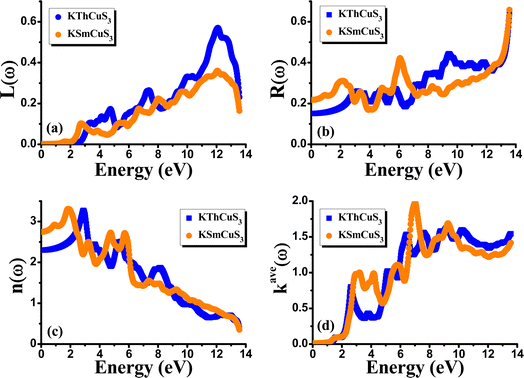 |
| | Fig. 6 The calculated (a) energy loss function (b) reflectivity (c) refractive index and (d) extinction coefficient for KMCuS3 (M = Th, Sm) materials. | |
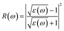
Materials have dielectric characteristics with positive permittivity [ε1(ω) > 0] at frequencies above a particular threshold and metallic properties with negative permittivity [ε1(ω) < 0] at frequencies below this threshold. The particular behavior that characterizes the substance describes it. The energy loss spectra, designated as L(ω), shed light on the precise frequency at which the material transitions between its metallic and dielectric properties. The maxima peaks for KThCuS3 and KSmCuS3 are visible in the energy loss spectra at 12.7 and 12.5 eV, respectively. Higher photon energy results in more prominent scattering mechanisms and other interactions. These interactions can cause energy to be transmitted to the material's phonons or other excitations, which causes the energy loss function to drop since the energy is distributed across many modes rather than directly contributing to it. Fig. 6(b) reflectivity spectra indicate the difference in the reflectance curves for the incident radiations with a polarization nature. We can calculate the optical reflectivity of these quaternary chalcogenides' materials with the help of the extinction coefficient and refractive index. An essential optical parameter with an inverse relationship to the energy loss function is the determined reflectivity spectrum R(ω). Because of the low energy region's low reflectivity spectrum, the infrared spectrum does not experience interband transitions. From R(0) of approximately 0.16 and 0.22 to extreme value of approximately 0.6 at 13.5 eV for both KThCuS3 and KSmCuS3, respectively, the R(ω) rises with energy. The visible and infrared regions show negligible reflection, whereas the ultraviolet area exhibits increased reflectivity for KMCuS3 (Th, and Sm). There were also noticeable variations in the ultraviolet range and a modest increase in the infrared (IR) spectrum. The existence of interband transitions might explain these variations.
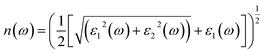
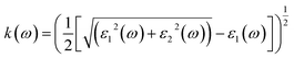
The term “refractive index” defines how light bends when traveling inside a material medium. For KThCuS3 and KSmCuS3, the computed values of n(0) which is a vital optical constant for the construction of the optoelectronic devices are 2.4 and 2.8, respectively. The energy bands in the material may begin to converge or blur at greater photon energies. The relationship between the extinction coefficient, k(ω), and photon energy is seen in Fig. 6(d). The ε2(ω) directly affects the extinction coefficient. The variation in the ε2(ω), thus exhibits a similar tendency (see Fig. 5(b)). Each KThCuS3 and KSmCuS3 compound has a threshold energy of 1.5 eV and 1.2 eV, respectively. The extinction coefficient value steadily rises with energy above these limits. Moreover, the k(ω), intense peaks in its spectra are identified at energies of 6.6 eV for KThCuS3 and 7.1 eV for KSmCuS3, and their corresponding peak values are provided. The possibility of stimulating electrons from the VB towards the CB increases as photon energy rises. These transitions can be more pronounced in materials with a clearly defined band structure at higher photon energy, resulting in stronger absorption and a higher extinction coefficient. The peak k(ω), values for KThCuS3 and KSmCuS3 compounds. The sharp peaks in the k(ω) values of KThCuS3 and KSmCuS3 compounds suggest that these materials have attained their maximum photon absorption capability at certain energies. If we continue to increase the photon energy, the k(ω) spectra will decrease dramatically, implying that the materials will be unable to absorb as much energy at higher photon energies.
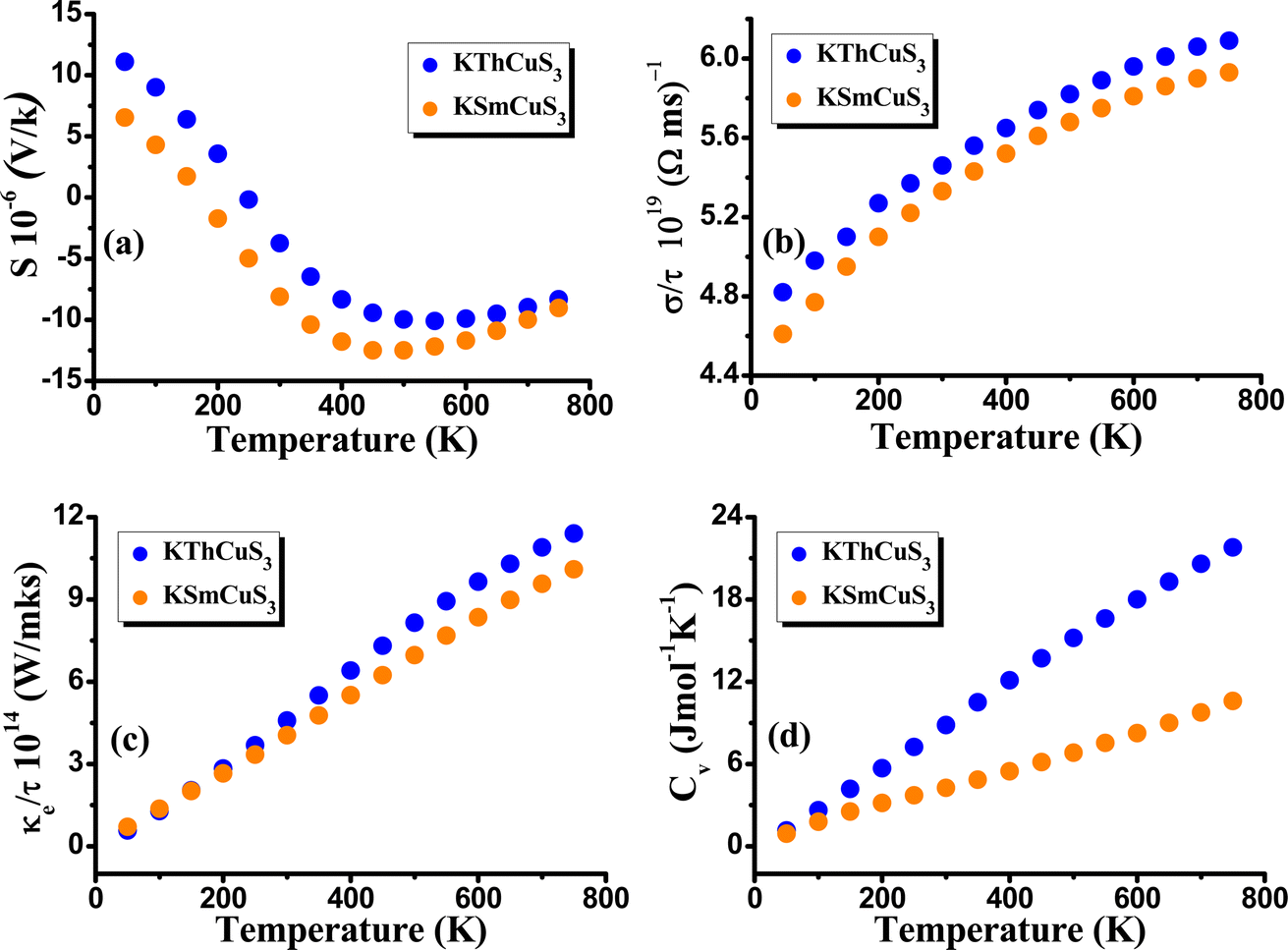
3.4 Thermoelectric properties
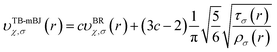
By using the BoltzTrap code47 and considering Fermi energy as a chemical potential at absolute zero temperature, we also pay attention to both quaternary compounds' thermoelectric properties to comprehend their potential employment in subsequent applications. The conductivity of the related materials is produced by the fact that the semiconductor materials contain a sizable number of electrons that can be energized to cross the band gap energy. As a result, energy gap values influence the electrical conductivity of semiconductor materials. It implies that a more accurate method of conducting electronic band structure calculations is needed for dependable evaluation of a material's electrical conductivity and other parameters to evaluate its potential for various applications. The key variables that determine the thermoelectric feature of materials are thermal conductivity, electrical conductivity, specific heat capacity, and Seebeck coefficient (S). In this current work, electrical conductivity, Seebeck coefficient, thermal conductivity, and specific heat capacity have been determined to explore the transport performance of KMCuS3 (M = Th, and Sm) compounds. The induced thermoelectric voltage caused by the difference in the temperature is determined from the Seebeck coefficient. Temperature has an impact on a material's carrier concentration or the quantity of charge carriers like electrons or holes. In some materials, activities like thermal excitation cause the generation of more charge carriers for the rise in temperature. As the material gets more conductive and the voltage produced across it as a result of a temperature gradient shrinks, it can result in a drop in the Seebeck coefficient if the carrier concentration rises sufficiently with temperature. In our example, the semiconducting nature was shown by the Seebeck coefficient at about 700 K, and determined to be equal to −9.12 × 10⁻⁶ V K−1 for KThCuS3 and −10.23 × 10⁻⁶ V K−1 for KSmCuS3. The fluctuation of the Seebeck coefficient (S) relating to temperature is shown in Fig. 7(a). The fluctuation in electrical conductivity (σ/τ) is depicted in Fig. 7(b). This characteristic of electrical conductivity with the temperature shows that the KMCuS3 compounds are semiconducting materials. At 200 K, KThCuS3 and KSmCuS3 were found to have electrical conductivities of 5.1 and 5.0 × 10¹⁸ (Ωms)−1, respectively.
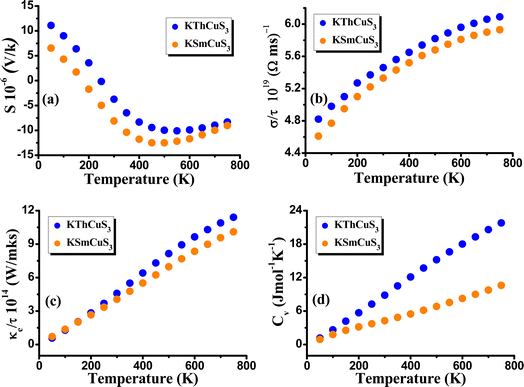 |
| | Fig. 7 The calculated (a) Seebeck coefficient (b) electrical conductivity (c) thermal conductivity and (d) specific heat capacity, for KMCuS3 (M = Th, Sm) materials. | |
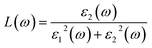
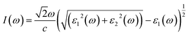
The compounds KThCuS3 and KSmCuS3 have the highest thermal conductivities at 800 K, with values of 6.5 and 5.8 (1014 W m−1 K−1 s−1), respectively. This could result in better electrical conductivity if the calculations show that the compound KMCuS3 possesses a larger density of states close to the Fermi level (the energy level at which electrons have a 50% likelihood of being occupied). This is due to a higher DOS near the Fermi level suggests that there are more electron-moving energy levels accessible, which helps to improve electrical conductivity. The thermal conductivity (κ) of these materials is a crucial characteristic that needs to be carefully controlled. For effective thermoelectric performance, a low thermal conductivity is vital because this aids in maintaining a high-temperature gradient. Fig. 7(c) illustrates the predicted thermal conductivity of the KMCuS3 quaternary chalcogenides. The electronic thermal conductivity rises as temperature rises, much like the electrical conductivity does. At 250 K, the electronic thermal conductivity of KThCuS3 is measured to be 4.5 × 10¹⁴ W m−1 K−1 s−1 and that of KSmCuS3 compounds to be 3.5 × 10¹⁴ W m−1 K−1 s−1. The thermal conductivities of KThCuS3 and KSmCuS3 compounds are 11.32 and 10.5 (1014 W m−1 K−1 s−1), respectively, at 800 K. Higher thermal energy causes the atoms to vibrate strongly at higher temperatures. The heat capacity of a material is influenced by these lattice vibrations. The lattice vibrations intensify with increasing temperature, increasing the specific heat capacity. At 800 K, KMCuS3 (M = Th, and Sm) has the highest specific heat capacity. At 800 K, KThCuS3 and KSmCuS3 have specific heat capacities of 22.5 and 12.5 Cv (Jmol−1 K−1), respectively. The amplified lattice vibrations, increased electronic excitations, phase transitions, electronic structural effects, and anharmonicity, are responsible for the compound KMCuS3 (M = Th, and Sm) increase in specific heat capacity along the temperature.
4. Conclusion
The PBE-GGA scheme predicted band gaps for the KSmCuS3 and KmThCuS3 were 0.61, and 2.03 eV, respectively. While the TB-mBJ computed band gaps for KSmCuS3 and KThCuS3 were 0.91, and 2.39 eV, respectively. The electronic band gaps were enhanced by higher coulomb repulsion between CB and VB brought about by the TB-mBJ approximation. When compared to KThCuS3, the band gap of KSmCuS3 was smaller as if the atoms are positioned in a way that promotes better electron contacts or energy level overlap. These compounds also display a semiconducting nature from their DOS calculations as the Fermi level splits these valence band and conduction band. The Tot-Cu states influence significantly to the valence band. The hybridization of the K-s/p, Sm-d/f, Cu-d, and S-p orbitals formed the valence band region. The Cu-d and S-p states contributions in the VB between −0.5 and 2.0 eV energy range are the source of the observed peak. The Tot-Sm states were the dominant contributor in the TDOS plot in the CB region. The Sm-d states contribute the most to PDOS plots in the CB region in the energy range from 0.9 eV up to 2.4 eV, followed by K-s/p and S-p states with smaller contributions. The valence electrons in these bands came from the potassium p orbitals, they contributed most to DOS peaks in the valence band region. The transition metal copper (Cu) is also distinguished by its partially filled d orbitals. Due to interactions with nearby atoms and the effects of crystal fields, the d orbitals in compounds can split into different energy bands. Additionally, for the compounds KThCuS3 and KSmCuS3, the spectra of ε1(ω) were seen as negative in the energy range of 7.5–11.5 eV and 5.5–7.2 eV, respectively which means that in this photon energy range, the materials exhibit metallic behavior and turn reflective in the direction of the incoming photons. In addition, the reason for the various peaks in the ε2(ω) may be connected to these PDOS for KMCuS3 (M = Th, and Sm) quaternary compounds. The energy bands in the material may begin to converge at greater photon energies. This may also result in a reduction in the density of transition energy levels, a reduction in absorption, and a corresponding reduction in the ε2(ω). Similar to this, as energy levels rise over threshold levels, optical conductivity gradually increases. Numerous sharp peaks were also seen in optical spectra, which were indicative of plasma excitations brought on by electrons moving from the VB to the CB. The KMCuS3 (M = Th, and Sm) quaternary chalcogenides could serve as potential materials for use in nano optoelectronic devices because of the wide absorption band and large absorption intensity. The visible and infrared regions showed negligible reflection, whereas the ultraviolet area exhibited an increased reflectivity for KMCuS3 (Th, and Sm). The refractive index rises when the incident light relates with electrons at lower photon energies (long wavelengths), causing energy absorption and electronic transitions. The characteristic of electrical conductivity with the temperature also confirmed the semiconducting nature of these compounds. The electronic thermal conductivity rises as temperature rises, in a similar way as the electrical conductivity.
Data availability
Data will be made available from the corresponding author upon reasonable request.
Conflicts of interest
The authors have no conflicts of interest to declare.
Acknowledgements
This work was funded by Researchers Supporting Project Number (RSPD2024R1047), King Saud University, Riyadh, Saudi Arabia.
References
- I. D. Olekseyuk, L. D. Gulay, I. V. Dydchak, L. V. Piskach, O. V. Parasyuk and O. V. Marchuk, J. Alloys Compd., 2002, 340, 141–145 CrossRef CAS.
- A. Bouarissa, A. Gueddim, N. Bouarissa and H. Maghraoui-Meherezi, Mater. Sci. Eng., C, 2021, 263, 114816 CrossRef CAS.
- S.-M. Kuo, Y.-M. Chang, I. Chung, J.-I. Jang, B.-H. Her, S.-H. Yang, J. B. Ketterson, M. G. Kanatzidis and K.-F. Hsu, Chem. Mater., 2013, 25, 2427–2433 CrossRef CAS.
- A. Samavati, A. Awang, Z. Samavati, A. Fauzi Ismail, M. H. D. Othman, M. Velashjerdi, G. Eisaabadi B. and A. Rostami, Mater. Sci. Eng., C, 2021, 263, 114811 CrossRef CAS.
- A. Abu Odeh, Y. Al-Douri, R. M. Ayub and A. S. Ibraheam, J. Alloys Compd., 2016, 686, 883–895 CrossRef CAS.
- X. Hu, X. Fan, B. Feng, D. Kong, P. Liu, C. Xu, Z. Kuang, G. Li and Y. Li, Mater. Sci. Eng., C, 2021, 263, 114846 CrossRef CAS.
- A. Bedjaoui, A. Bouhemadou, S. Aloumi, R. Khenata, S. Bin-Omran, Y. Al-Douri, F. Saad Saoud and S. Bensalem, Solid State Sci., 2017, 70, 21–35 CrossRef CAS.
- T. V. Vu, A. A. Lavrentyev, B. V. Gabrelian, V. A. Tkach, K. D. Pham, O. V. Marchuk, O. V. Parasyuk and O. Y. Khyzhun, Solid State Sci., 2020, 104, 106287 CrossRef CAS.
- M. Mesbahi, F. Serdouk and M. Benkhedir, Acta Phys. Pol., A, 2018, 134, 358–361 CrossRef CAS.
- C. W. Sinagra, F. O. Saouma, C. O. Otieno, S. H. Lapidus, J.-H. Zhang, A. J. Craig, P. Grima-Gallardo, J. A. Brant, K. A. Rosmus, K. E. Rosello, J. I. Jang and J. A. Aitken, J. Alloys Compd., 2021, 888, 161499 CrossRef CAS.
- F.-J. Fan, B. Yu, Y.-X. Wang, Y.-L. Zhu, X.-J. Liu, S.-H. Yu and Z. Ren, J. Am. Chem. Soc., 2011, 133, 15910–15913 CrossRef CAS PubMed.
- F. Sarcan, M. Aydin, F. Kuruoğlu, O. Donmez, S. Yildirim and A. Erol, Mater. Sci. Eng., C, 2021, 272, 115322 CrossRef CAS.
- A. Swarnkar, W. J. Mir, R. Chakraborty, M. Jagadeeswararao, T. Sheikh and A. Nag, Chem. Mater., 2019, 31, 565–575 CrossRef CAS.
- S. Niu, H. Huyan, Y. Liu, M. Yeung, K. Ye, L. Blankemeier, T. Orvis, D. Sarkar, D. J. Singh, R. Kapadia and J. Ravichandran, Adv. Mater., 2016, 29, 1604733 CrossRef PubMed.
- N. O. Azarapin, N. A. Khritokhin, V. V. Atuchin, A. A. Gubin, M. S. Molokeev, S. Mukherjee and O. V. Andreev, Crystals, 2023, 13, 903 CrossRef CAS.
- W. Meng, B. Saparov, F. Hong, J. Wang, D. B. Mitzi and Y. Yan, Chem. Mater., 2016, 28, 821–829 CrossRef CAS.
- Y.-Y. Sun, M. L. Agiorgousis, P. Zhang and S. Zhang, Nano Lett., 2015, 15, 581–585 CrossRef CAS PubMed.
- B. Kinzeeva, G. Turlakov, I. Moggio, E. Arias, G. Rodríguez, M. Herrera, T. Cooper, M. Ottonelli and R. F. Ziolo, Mater. Sci. Eng., C, 2021, 263, 114779 CrossRef CAS.
- N. Kodan and B. R. Mehta, J. Alloys Compd., 2024, 970, 172496 CrossRef CAS.
- A. Taya, P. Rani, J. Thakur and M. K. Kashyap, Vacuum, 2019, 160, 440–444 CrossRef CAS.
- N. A. N. M. Nor, M. A. H. Razali, W. H. A. W. K. Annuar, N. N. Alam, F. N. Sazman, N. H. M. Zaki, A. S. Kamisan, A. I. Kamisan, M. H. Samat, A. M. M. Ali, O. H. Hassan, B. U. Haq, M. Z. A. Yahya and M. F. M. Taib, Phys. B, 2024, 673, 415450 CrossRef CAS.
- B. V. Gabrelian, A. A. Lavrentyev, T. V. Vu, K. F. Kalmykova, L. N. Ananchenko, V. A. Tkach, O. V. Parasyuk and O. Y. Khyzhun, Mater. Today Commun., 2020, 23, 100828 CrossRef CAS.
- W. Yin, K. Feng, W. Hao, J. Yao and Y. Wu, Inorg. Chem., 2012, 51, 5839–5843 CrossRef CAS PubMed.
- K. M. Wong, W. Khan, M. Shoaib, U. Shah, S. H. Khan and G. Murtaza, J. Electron. Mater., 2017, 47, 566–576 CrossRef.
- L. R. Dalton, P. A. Sullivan and D. H. Bale, Chem. Rev., 2009, 110, 25–55 CrossRef PubMed.
- M. Abubakr, Z. Abbas, A. Naz, H. M. Khalil, M. A. Khan, H. Kim, K. Khan, M. Ouladsmane, S. Rehman, D. Kim and M. F. Khan, Opt. Quantum Electron., 2023, 55, 849 CrossRef CAS.
- M.-L. Liu, I.-W. Chen, F.-Q. Huang and L.-D. Chen, Adv. Mater., 2009, 21, 3808–3812 CrossRef CAS.
- R. Chetty, A. Bali and R. C. Mallik, Intermetallics, 2016, 72, 17–24 CrossRef CAS.
- H. Matsushita, T. Maeda, A. Katsui and T. Takizawa, J. Cryst. Growth, 2000, 208, 416–422 CrossRef CAS.
- M. Cao, L. Li, W. Z. Fan, X. Y. Liu, Y. Sun and Y. Shen, Chem. Phys. Lett., 2012, 534, 34–37 CrossRef CAS.
- C. Li, M. Cao, J. Huang, L. Jun Wang and Y. Shen, Mater. Lett., 2015, 140, 170–173 CrossRef CAS.
- H. Guo, Y. Li, X. Fang, K. Zhang, J. Ding and N. Yuan, Mater. Lett., 2016, 162, 97–100 CrossRef CAS.
- L. Shi, C. Wu and J. Ding, J. Alloys Compd., 2016, 683, 46–50 CrossRef CAS.
- Q. Zhang, H. Deng, L. Chen, J. Tao, J. Yu, P. Yang and J. Chu, Mater. Lett., 2017, 193, 206–209 CrossRef CAS.
- M. G. Brik, I. V. Kityk, O. V. Parasyuk and G. L. Myronchuk, J. Phys.: Condens. Matter, 2013, 25, 505802 CrossRef CAS PubMed.
- T. V. Vu, A. A. Lavrentyev, B. V. Gabrelian, K. D. Pham, C. V. Nguyen, K. C. Tran, H. L. Luong, M. Batouche, O. V. Parasyuk and O. Y. Khyzhun, J. Electron. Mater., 2018, 48, 705–715 CrossRef.
- A. Tombak, T. Kilicoglu and Y. S. Ocak, Renew. Energy, 2020, 146, 1465–1470 CrossRef CAS.
- T. Hirai, K. Kurata and Y. Takeda, Solid-State Electron., 1967, 10, 975–981 CrossRef CAS.
- L. P. Marushko, L. V. Piskach, O. V. Parasyuk, I. D. Olekseyuk, S. V. Volkov and V. I. Pekhnyo, J. Alloys Compd., 2009, 473, 94–99 CrossRef CAS.
- I. D. Olekseyuk, L. D. Gulay, I. V. Dydchak, L. V. Piskach, O. V. Parasyuk and O. V. Marchuk, ChemInform, 2002, 33, 9 CrossRef.
- R. Basu, M. Patel, S. Bhattacharya, R. Bhatt, M. Roy, A. Singh, D. K. Aswal and S. K. Gupta, AIP Conf. Proc., 2013, 1536, 1227–1228 CrossRef CAS.
- M. Liu, I. Chen, F. Huang and L. Chen, Adv. Mater., 2009, 21, 3808–3812 CrossRef CAS.
- W. Li, M. Ibáñez, R. R. Zamani, N. García-Castelló, S. Gorsse, D. Cadavid, J. D. Prades, J. Arbiol and A. Cabot, CrystEngComm, 2013, 15, 8966 RSC.
- A. D. Becke and E. R. Johnson, J. Chem. Phys., 2006, 124, 174104 CrossRef PubMed.
- F. Tran, P. Blaha and K. Schwarz, J. Phys.: Condens. Matter, 2007, 19, 196208 CrossRef.
- B. Gul, M. S. Khan, A. A. lfseisi and H. Ahmad, Phys. Scr., 2023, 98, 115927 CrossRef.
- G. K. H. Madsen and D. J. Singh, Comput. Phys. Commun., 2006, 175, 67–71 CrossRef CAS.
|
| This journal is © The Royal Society of Chemistry 2024 |
Click here to see how this site uses Cookies. View our privacy policy here. 
 Open Access Article
 This Open Access Article is licensed under a Creative Commons Attribution-Non Commercial 3.0 Unported Licence
 *a,
Banat Gulb,
Abdelhay Salah Mohamedc and
Faheem Abbasd
*a,
Banat Gulb,
Abdelhay Salah Mohamedc and
Faheem Abbasd


 are the electric conductivity, the temperature gradients, Seebeck coefficient, external electric field, and the electrical current density, respectively.