
 Open Access Article
 This Open Access Article is licensed under a Creative Commons Attribution-Non Commercial 3.0 Unported Licence
High-performance ultraviolet detector based on self-assembled 3D/2D perovskite heterostructure†
Haiyan Wang *ab,
Mengxin Ningb,
Qiaohe Wangb,
Yachuan Liangab,
Sen Lib,
Zijiong Lia,
Lingli Wang*a,
Yan Wangab and
Liying Jiangab
*ab,
Mengxin Ningb,
Qiaohe Wangb,
Yachuan Liangab,
Sen Lib,
Zijiong Lia,
Lingli Wang*a,
Yan Wangab and
Liying Jiangab
aAcademy for Quantum Science and Technology, Zhengzhou University of Light Industry, Zhengzhou 450002, PR China. E-mail: wanghaiyan@zzuli.edu.cn
bSchool of Electronics and Information, Zhengzhou University of Light Industry, Zhengzhou 450002, PR China
First published on 27th August 2024
Abstract
Heterogeneous assembly of metal halide perovskites (MHPs) structures offers convenience for promoting the interfacial properties of perovskite heterojunctions, which have been widely used in the new generation of photoelectric devices. In this study, three-dimensional (3D) CsPbBr3 quantum dots (CPB QDs) were epitaxially grown on two-dimensional (2D) (BA)2PbBr4 nanoplates (BPB NPs) via self-assembly in a toluene mixing solution. The morphological, structural, and optical properties of the synthesized structure reveal that a highly-qualified interface and coherence were formed between the two different perovskites. These heterostructures (HSs) facilitate the separation and transportation of electrons and holes in opposite directions. Based on this property, a high-performance ultraviolet light detector was fabricated by depositing a layer of CPB@BPB film on a textured silicon (T-Si) substrate. The prepared CPB@BPB/T-Si detector has shown enhanced properties i.e. quick response time, high responsivity (6.9 A W−1), high detection rate (3.17 × 10⁹ jones), and low detection limit (0.24 μW cm−2). This enhanced performance could be attributed to the large light-absorbing area, effective carrier transport channels in BPB NPs, and improved interfacial properties of the CPB@BPB HS.
1. Introduction
Due to their superior photoelectric conversion capability, metal halide perovskites (MHPs) are becoming the most promising candidates in photoelectric devices, such as solar cells,1–3 photo/X-ray detectors,4–6 light-emitting diodes,7,8 and lasers,9 etc. Similar to other semiconductors, perovskites can also form heterostructures (HSs) by stacking one on another structure. It has been established that HSs not only enhance the internal quantum efficiency but also reduce the non-radiative recombination loss. This results in improving the overall electro-optical conversion efficiency of MHPs.10–13Carrier transport properties and charge-carrier dynamics in perovskite HSs are highly dependent on the interfacial properties of perovskite structures. However, previously developed perovskite HSs were fabricated via solution-processed polycrystalline thin films. In these structures, the lattice structure, crystallinity, and direction are different between the two working perovskites. It is challenging to regulate the interfacial properties of the heterojunctions by adjusting the perovskite layers. Therefore, the heterogenous assembly of perovskites is attracting researchers due to the highly qualified interfaces and strong coherence formed between the two working perovskites.14,15
Due to their weak tolerance against lattice distortion and relatively high formation energy, the heterogeneous assembly of perovskites needs extra energy, such as heating or light irradiation, to initiate the soldering at interfaces.16,17 Recently, an interesting epitaxial assembly of three-dimensional (3D) CsPbBr3 on two-dimensional (2D) (PEA)2PbBr4 has been reported by Zhu, et al.18 They observed that the welding takes place at room-temperature with the assistance of the residual PEA+ ions in the precursor solution. In the reported structure, the PEA+ ions replaced the oleic acid and the oleylamine molecules covered the CsPbBr3 quantum dots (QDs). Moreover, it also served as a bridge between the [PbBr6]4− octahedra in CsPbBr3 and (PEA)2PbBr4. Interestingly, most of the CsPbBr3 QDs are grown on the (PEA)2PbBr4 plates in a specific direction due to the control of (PEA)2PbBr4 to CsPbBr3. The fabrication of perovskite HSs by this method does not have any high-temperature risk during the process. In order to shorten the fabrication process, Zhu and his team19 further developed a simple one-step solution method to prepare 3D/2D CsPbBr3/PEA2PbBr4 perovskite HSs by addition of a homogeneous dimethyl formamide solution of PEABr, PbBr2, and CsBr to toluene under vigorous stirring. They denounced that CsPbBr3 and PEA2PbBr4 nucleated and grew separately in solution and then came together to form the HSs. However, the epitaxial welding of CsPbBr3 on PEA2PbBr4 in this method might have been supported by another reason, because oleic acid/oleylamine (OA/OLA) wasn't used in the solution, and thus the replacement of OA/OLA by PEA+ didn't happen.
Here, we have to notice that, in the one-step method, CsPbBr3 and PEA2PbBr4 both have a nanosized structure, and high surface energy might have taken the primary responsibility for the heterogeneous assembly between the nanosized perovskites. Crystal growth via oriented aggregation of primary nanoparticles/clusters has been found in a wide range of materials.20–24
To clarify if the high surface energy of the nanosized perovskites can overcome the welding barrier and initiate the heterogeneous soldering at the interface, we used CsPbBr3 (CPB) quantum dots and (BA)2PbBr4 (BPB, BA = n-butylammonium) nanoplates to form 3D/2D perovskite heterostructures via the post-growth method in this study. The morphology, lattice structure, and optical properties of the synthesized CPB@BPB HS were studied carefully. Moreover, to validate the effect of HSs on the generated carriers in perovskites, an ultraviolet light detector based on CPB@BPB HS was fabricated. Enhanced properties were observed in the prepared detectors i.e. high responsivity of 6.9 A W−1, high detection rate of 3.17 × 10⁹ jones and low detection limit of 0.24 μW cm−2. The excellent performance of CPB@BPB, which was attributed to the enhanced light absorption and the accelerated carrier transport in the heterostructure, indicates that a high-quality interface was formed between the two working perovskites.
2. Experiment
2.1 Synthesis of materials and detectors
2.2 Characterization methods
The morphology and structure of the CPB QDs and CPB@BPB HSs were studied using high-resolution transmission electron microscopy (HRTEM, Philips CM-20 microscope) and selected area electron diffraction (SAED), respectively. Field emission scanning electron microscopy (FE-SEM, JSM-7001F, Japan) and X-ray diffraction (XRD, SmartLab SE X-ray diffractometer) analysis were conducted to study the morphology and lattice structure of the CPB@BPB film deposited on T-Si. The absorption and photoluminescent properties of the samples were characterized using a UV-visible spectrophotometer (UH4150, China) and a fluorescence spectrometer (Horiba; Fluoro Max-4) equipped with an integrated sphere (Horiba; Quanta-φ), respectively. The light-response test was executed in a black box. The photocurrent and dark current were collected using a digital source-Meter (Keithley 2400).3. Results and discussion
3.1 Material characterization
The schematic for synthesis of CsPbBr3 QDs is illustrated in Fig. 1(a). DMF solutions of CsBr and PbBr2 were added dropwise into toluene under vigorous stirring at 80 °C. The solution was then cooled in ice water, after which it turned into yellowish green which was then centrifuged to separate large particles of CsPbBr3. After the separation of CsPbBr3 particles, green CPB QDs dispersion was obtained. Transmission electron microscopic studies revealed that the size of CPB QDs is in the range of 10–20 nm as shown in Fig. 1(b). Moreover, HRTEM and SAED studies indicate that CsPbBr3 has an orthorhombic structure (space group of pnma) at room temperature as displayed in Fig. 1(c) and (d) respectively.27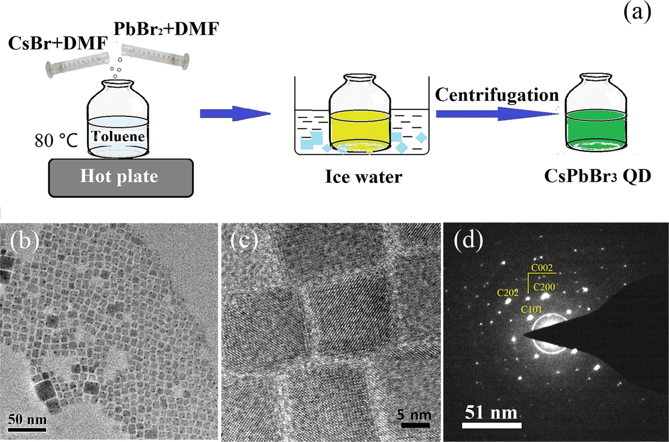 | ||
| Fig. 1 (a) Schematic representation of the synthesis of CPB QDs. (b) TEM image, (c) HRTEM, and (d) SAED pattern of the CPB QDs (C represents CPB). | ||
Self-assembled CPB@BPB heterostructure was obtained by mixing the toluene solution of CPB QDs and BPB NPs. The schematic of the process is displayed in Fig. 2(a). To study the morphology and structure of CPB@BPB, HRTEM and SAED analysis were carried out. HRTEM studies revealed that CPB QDs were absorbed on the surface of thin BPB NPs as shown in Fig. 2(b). Interestingly, CsPbBr3 is arranged in a particular direction on the surface of the (BA)2PbBr4 plate, as shown in the red circle in Fig. 2(b). The lattice structure of (BA)2PbBr4 at the surface have important influence to the heterogenous assembly of the CsPbBr3 QDs, determining the direction of the welded quantum dots. A coherence was formed between the 2D and the 3D perovskites, which provide convenience for regulating the interfacial properties of the heterojunctions by adjusting the perovskite layers. This is also confirmed by the SAED results in Fig. 2(c). The lattice mismatch between CsPbBr3 (002) and (BA)2PbBr4 (220) planes is ∼0.1%, which resulted in overlapping of SAED spots. The oriented assembly of CsPbBr3 on (BA)2PbBr4, could be attributed to the high energy of the perovskites21–24 and periodic networks of corner-shared [PbBr6]4− octahedron.
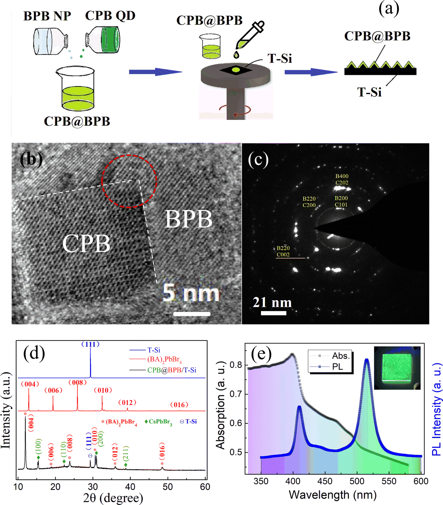 | ||
| Fig. 2 (a) Schematic illustration of the fabrication of CPB@BPB HSs and CPB@BPB film on T-Si substrate. (b) HRTEM, and (c) SAED pattern of the CPB@BPB HSs. (d) XRD patterns of the pristine (BA)2PbBr4 powder, the silicon substrate and the CPB@BPB film. (e) Optoelectronic properties of CPB@BPB HS. | ||
The lattice structure of the pristine (BA)2PbBr4 powder, the silicon substrate, and the CPB@BPB film was characterized using XRD analysis. The reflexes at the angles of 15.5, 22.4, 30.9 and 38.8 are assigned to the (100), (110), (200) and (211) plane of the orthorhombic CsPbBr3 (JCPDS 18-0364), respectively, based on the perfect match. This structure can be confirmed by the HRTEM results of the CsPbBr3 QDs. The diffraction peak located at 28.8° in the pattern of the final CPB@BPB/T-Si can be easily recognized that it comes from the (111) plane of silicon by referring the pattern of the T-Si substrate. The reflexes located at 12.0°, 23.9°, 36.0° and 48.1° are respectively assigned to the (004), (008), (012) and (016) plane of (BA)2PbBr4 by us because of the characteristics of periodic distribution, which is the typical feature of diffraction peaks in layered 2D perovskites (it can be found in the pattern of the pristine (BA)2PbBr4). The peaks located at 18.8° and 30.6° are accordingly assigned to the (006) and (010) planes of (BA)2PbBr4, respectively. Compared with the pattern of the pristine (BA)2PbBr4, the diffraction peaks of (BA)2PbBr4 in the CPB@BPB film move to the smaller angles, indicating that there is a larger distance between the (0 0 2n) plane in the nanosized (BA)2PbBr4 sample.
In order to clarify the origin of the enlarged inter-layer space of the (BA)2PbBr4 nanoplates in CPB@BPB, the lattice structure of the nanosized BA2PbBr4 sample was tested separately using XRD analysis (Fig. 1S†). Compared with the pristine BA2PbBr4, the reflexes of the nanosized BA2PbBr4 sample shift to lower angles also, as same as the BA2PbBr4 nanoplates in the CPB@BPB heterostructure, indicating that the increased inter-layer space is not caused by the formation of the CPB@BPB heterostructure, but is an intrinsic property of the nanosized 2D (BA)2PbBr4. The formation of the heterostructure might have influence to the lattice structure of the 2D BA2PbBr4, but it should be weak, especially in the out-plane direction. This kind of weak effect has been proved in Zhu et al.'s work,19 where no obvious shift was found in the PEA2PbBr4 (0 0 2n) reflexes, even though a clear lattice pattern extending from CPB to PPB was observed in the in-plane direction. Therefore, the enlarged inter-layer space would have been caused by the reduction of size of the (BA)2PbBr4 nanoplates in the out-plane direction. XRD patterns show characteristic diffraction peaks of both CsPbBr3 and (BA)2PbBr4 which indicates the successful loading of CsPbBr3 QDs on (BA)2PbBr4 NPs.
In order to evaluate the optical properties of the as-prepared CPB@BPB sample, absorption and photoluminescence (PL) spectroscopy studies were carried out. The absorption spectrum of a CPB@BPB dispersion is displayed in Fig. 2(e). The peak at 410 and 500 nm can be assigned to BPB and CPB, respectively. When the sample was excited with 365 nm laser, two emission peaks at 411 and 521 nm were observed, which could be attributed to BPB and CPB, respectively.28,29 There is an additional band at around 430–440 nm in the PL spectrum which might have come from the electronic interaction between the inorganic layers in the layered BPB single crystals.25,30,31 This band has been found in the nanosized BA2PbBr4 sample also (Fig. 2S†), however, its intensity is much lower than that of the pristine BA2PbBr4 crystals due to the enlarged inter-layer space. There is no stokes shift for the BPB NPs, however, there is an obvious shift of 100 meV between the absorption and emission states of CPB QDs. Some experiments have revealed that a confined hole state is formed in the CsPbBr3 nanoparticles. This hole state could be the reason of stokes shift that can be tuned via nanosized crystal.32 The inset of Fig. 2(e) shows daylight and photoluminescence photographs of the synthesized CPB@BPB film deposited on glass. This indicates that the present method can be used large scale production.
SEM images of bare T-Si and T-Si covered with a layer of CPB@BPB film are shown in Fig. 3. It can be observed that bare T-Si has a rough surface (roughness is 800) which leads to increase in the surface area of the silicon substrate by 2 times. A thin layer of CPB@BPB film was uniformly deposited on the surface of T-Si. Consequently, the photo-absorbing area of synthesized CPB@BPB film is about 2 times greater than a planar film, which could be beneficial for improved photo-detection in the CPB@BPB/T-Si detector.
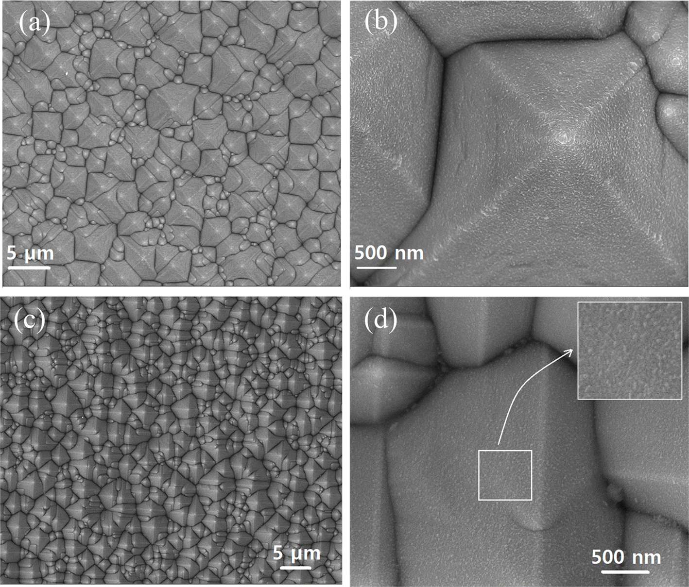 | ||
| Fig. 3 FE-SEM images of T-Si (a) and (b) and CPB@BPB/T-Si (c) and (d). | ||
3.2 Performance of CPB@BPB/T-Si photo detector
Initially, the light response of the prepared CPB@BPB/T-Si detector to 405 nm of UV light was studied using photocurrent outflow from the detector at 0 bias. Fig. 4(a) and (b) show the measurement diagram and results, respectively. It is evident that when the detector is illuminated by UV light (405 nm) there is an obvious increase in the current. Moreover, when the intensity of light was increased from 0.5 to 1.65 mW cm−2, a steady increase in the photocurrent of CPB@BPB/T-Si detector was observed. This typical behavior of photodetector indicates that the greater the number of photons, the more is the number of photo-generated charge carriers in the device.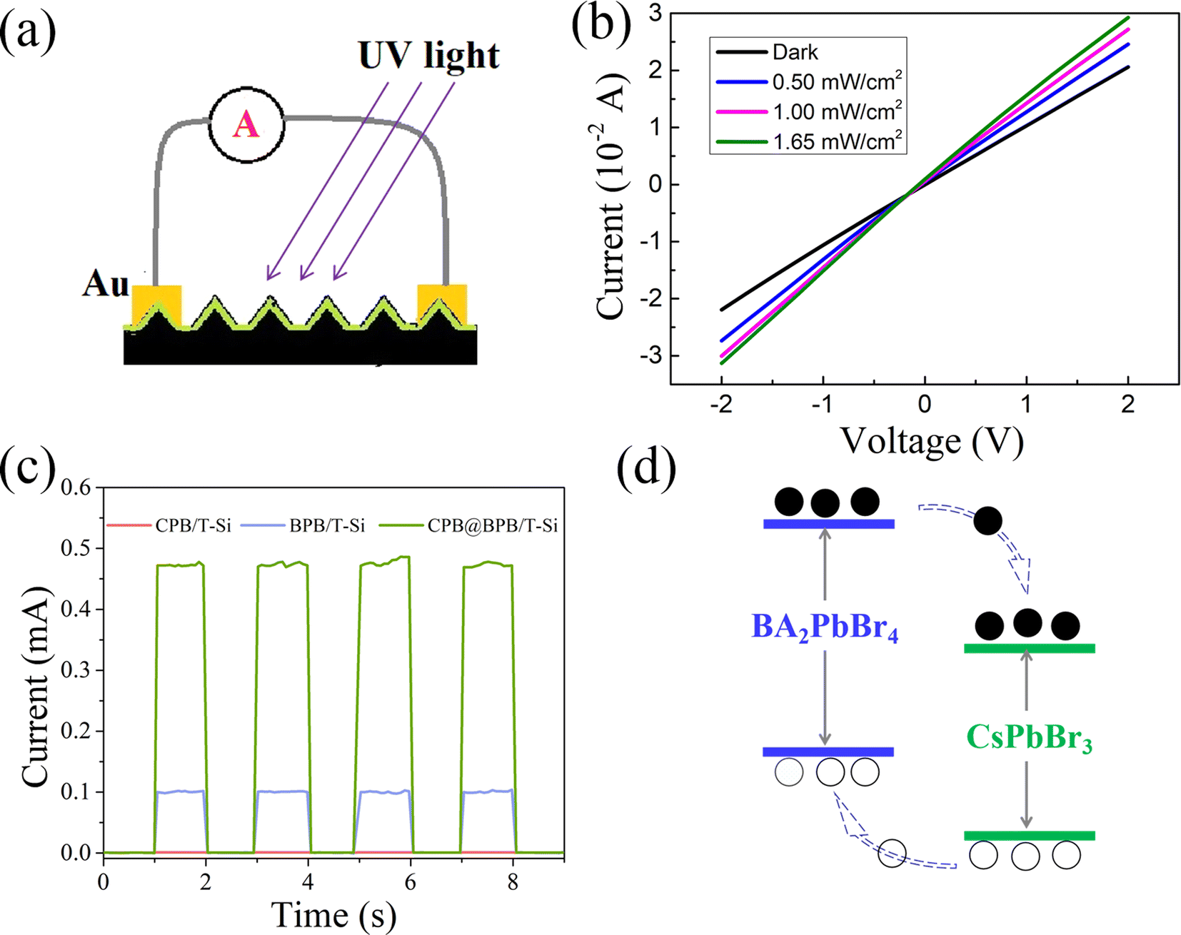 | ||
| Fig. 4 (a) Schematic diagram of device structure and photodetection process of the CPB@BPB/T-Si photodetector. (b) I–V curves of photodetectors based on CPB@BPB/T-Si under different powers of 405 nm laser irradiation at 0 bias. (c) I–t curves of photodetectors based on CPB/T-Si, BPB/T-Si and CPB@BPB/T-Si under 405 nm laser irradiation and 1100 μw cm−2 illumination intensity. (d) Schematic diagram of the band alignment of CPB and BPB, and the charge transfer process of the CPB/PPB HSs excited with a 405 nm laser. | ||
In order to evaluate the synergistic effect of CPB and BPB on charge carrier transportation, the photocurrent of the two reference detectors, CPB/T-Si and BPB/T-Si, was also measured. All of the detectors have the same device structure, light-absorbing area, and interdigital gold electrode. When the detectors were illuminated by 405 nm laser with intensity of 1.1 mW cm−2 at 0 bias, the photocurrent of them was measured. The results indicate that the photocurrent of CPB@BPB/T-Si drastically increased than that of the other 2 detectors as shown in Fig. 4(c). More specifically, the photocurrent of detector CPB@BPB/T-Si is 5.2 and 470 times higher than that of BPB/T-Si and CPB/T-Si detectors, respectively.
The outstanding performance of CPB@BPB/T-Si could be attributed to the plate-like structure of BPB NPs. These plate like BPB NPs provides carrier transport channels for the unconnected CPB QDs in the CPB@BPB film. In addition, the heterostructure might also have facilitated the transfer of the generated charge carrier. Moreover, the energy levels of CPB and BPB NPs have also been reported33,34 which reveals that they have type-II band alignment between them. This can also promote the electron–hole separation and transfer in opposite directions, thus improving the photodetection efficiency.
The selectivity of the photodetector was evaluated by measuring the responses of the detector to incident lights with different wavelengths. The on/off ratio of the CPB@BPB/T-Si detector under laser irradiation from 254 to 850 nm is shown in Fig. 5(a). The intensity of the light was maintained at 1.1 mW cm−2 during the whole measurement, the responsivity (R) of the detector was calculated using a formula:
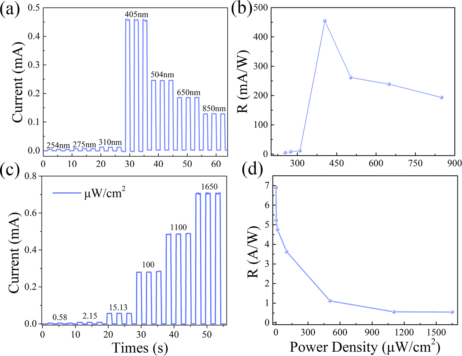 | ||
| Fig. 5 (a) I–t curves of the CPB@BPB/T-Si detector under the same power and different wavelength laser irradiation. (b) Responsiveness curve of the device under different wavelength illumination; (c) I–t curves of the CPB@BPB/T-Si detector under different power of 405 nm wavelength laser illumination; (d) responsiveness curve of the device under different power of illumination. | ||
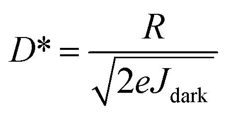
To evaluate the light detection capability of the detector in visible region, photocurrent tests were conducted under laser irradiation of different powers at constant wavelength of 405 nm. The Fig. 5(c) shows the variation of photocurrent with the intensity of light at 0 bias. The responsivity of the detector was determined under different conditions. The results revealed that value of R gradually decreases with increasing light intensity, Fig. 5(d). In addition, the CPB@BPB/T-Si detector has shown excellent performance towards detection of weak light signals. Furthermore, the maximum responsivity was 6.896 A W−1 which was observed under irradiation of UV light with intensity of 0.58 μW cm−2. Under these conditions, the photodetector has a high detection rate of 3.17 × 10⁹ jones which was calculated by using following formula:
The response rate of a photodetector refers to the time taken to rise the device's photocurrent from 10% to 90% peak value, also known as the rise time (named as tr). In addition, the time taken to drop the photocurrent from 90% to 10% is referred as the fall time (named as tf). A faster response speed makes the detector more suitable for detecting rapidly changing light signals. Fig. 6(a) reveals that the CPB@BPB/T-Si detector has fast response speed, with tr and tf value of 7.44 and 58 ms, respectively.
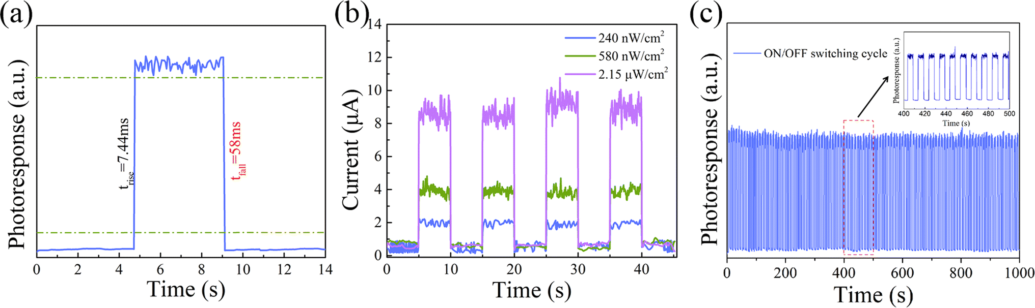 | ||
| Fig. 6 (a) Response time of the CPB@BPB/T-Si photodetector; (b) I–t curves of photocurrent under different light intensities; (c) recyclable switching operation of photocurrent response. | ||
The light detection capacity of the detector is displayed in Fig. 5(c) and (d). The results indicate that CPB@BPB/T-Si has enhanced performance towards detecting weak light signals. Thus, detection limit of the detector was measured which is an important parameter for evaluating of the performance of photodetectors. It is worth noting that the CPB@BPB/T-Si detector achieves an incredibly low detection limit of 0.24 μW cm−2 to the 405 nm UV light, as shown in Fig. 6(b).
Moreover, the photoactive stability of the prepared CPB@BPB/T-Si detector was also measured. The results demonstrate that the detector possesses long-term photoactive stability, as represented in Fig. 6(c). Even after “on/off” testing of the switch for 1000 s, the detector's photocurrent has not shown any significant changes, which is crucial for the widespread application of photonic devices.
The important parameters of the CPB@BPB/T-Si detector compared with other 2D perovskite and 3D/2D heterostructural detectors are shown in Table 1. It can be concluded that the CPB@BPB/T-Si detector has relative high responsivity and ultra low detection limit to UV Light compared with the current sensors.
| Material | Wavelength (nm) | Responsivity (A W−1) | Detection rate (Jones) | Detection limit (μW cm−2) | Ref. |
|---|---|---|---|---|---|
| CPB@BPB/T-Si | 405 | 6.9 | 3.17 × 10⁹ | 0.24 | This work |
| (BA)2PbBr4 | 447 | 0.381 | 9.01 × 10¹⁰ | 0.5 | 38 |
| (BA)2PbBr4 | 400 | 0.045 | 1.08 × 10¹² | 2750 | 39 |
| (BA)2PbBr4 | 470 | 2100 | — | 1000 | 40 |
| (C8H11FN)2PbBr4 | 254 | 0.288 | 1.6 × 10¹¹ | 2.13 × 10⁵ | 41 |
| (BA)2Pb(Br0.9Cl0.1)4 crystal | 340 | 3.19 × 10⁻³ | 3.87 × 10¹¹ | 5.4 | 42 |
| (BA)2Pb(Br0.9Cl0.1)4 film | 340 | 3.5 × 10⁻⁵ | 1.3 × 10¹⁰ | — | 42 |
| CsPbBr3/(PEA)2PbBr4 | 405 | 2.15 × 10⁻⁵ | — | — | 19 |
| (C4H9NH3)2PbBr4/MAPbBr3 | 428 | — | 9.3 × 10¹¹ | 1200 | 43 |
| (4-AMP)(MA)2Pb3Br10/MAPbBr3 | 405 | 1.5 × 10⁻³ | 3.8 × 10¹⁰ | 180 | 44 |
The excellent light-detecting performance of CPB@BPB/T-Si detectors can be attributed to several factors. One is the large light-absorbing area which is contributed by the textured silicon substrate. The CPB@BPB film has an enlarged photo-absorbing area which is about 2 times greater than the planar CPB@BPB film. More light absorbing materials can generate more charge carrier which are the critical contributor of photocurrent.37 Another reason is the presence of effective carrier transport channels in BPB NPs which are beneficial in the efficient and rapid transportation of the carriers in the dispersed CPB NCs. This can also be confirmed by the extremely low on/off ratio of CPB/T-Si. The highly qualified heterointerface also contributes to high on/off ratio of the CPB@BPB/T-Si detector. It has been reported that carrier transport properties and charge carrier dynamics in perovskite HSs are highly dependent on the quality of the interface.45,46 It can be concluded from HR-TEM and SAED analysis of CPB@BPB that CPB QDs were absorbed on the BPB NPs in a specific direction. Moreover, a highly qualified coherent interface was formed between the two working semiconductors. As the electron–hole separation and transfer is improved in the heterostructures, therefore, photodetection performance of the synthesized CPB@BPB/T-Si detector was enhanced greatly.
4. Conclusion
In summary, a heterostructure CsPbBr3@(BA)2PbBr4 nanocomposite was successfully synthesized via self-assembly method. The synthesized heterostructure has high surface energy and similar periodic networks of the two nano-sized perovskites. Moreover, a highly qualified interface with coherence was created between the two working semiconductors, which can offer convenience for regulating the properties of the heterostructure by adjusting any of the perovskite layer. With the aid of heterostructure in electron–hole separation and transfer, a highly efficient ultraviolet light detector was fabricated by depositing a layer of CsPbBr3@(BA)2PbBr4 film on a textured silicon substrate. High responsivity, rapid response speed, low detection limit, and long-time stability were achieved in the prepared CPB@BPB detector. Excellent performance of the as prepared detector could be attributed to the larger light-absorbing area due to the rough texture of silicon substrate. The current study presents a convenient method for fabrication of perovskite heterostructure that facilitates efficient carrier transport, thereby enabling the development of sensitive and robust UV light detectors.Data availability
The authors confirm that the data supporting the findings of this study are available within the article and/or its ESI.†Author contributions
Haiyan Wang: writing the first draft, funding acquisition, project administration; Mengxin Ning: investigation, data curation, methodology; Qiaohe Wang: investigation, formal analysis; Yachuan Liang, formal analysis; Sen Li: formal analysis; Zijiong Li: formal analysis; Lingli Wang: funding acquisition; Yan Wang: formal analysis; Liying Jiang: writing – review & edit.Conflicts of interest
No conflict of interest exists.Acknowledgements
This work is supported by Key Research & Development and promotion projects in Henan Province (grant numbers 212102210134, 222102210038), the Henan Science and Technology Major Project of the Department of Science And Technology of Henan Province (No. 241100210400) as well as Maker Space project in Zhengzhou University of Light Industry (grant number 2021ZCKJ220).References
- Y. Fu, H. Zhu, J. Chen, M. P. Hautzinger, X. Y. Zhu and S. Jin, Nat. Rev. Mater., 2019, 4, 169–188 CrossRef CAS.
- S. Masi, A. Rizzo, R. Munir, A. Listorti and S. Colella, Adv. Energy Mater., 2017, 7, 1602600 CrossRef.
- W. Yang, B. Park, E. Jung, N. Jeon and S. Seok, Science, 2017, 356, 376–1379 Search PubMed.
- J. Zhou and J. Huang, Adv. Sci., 2018, 5, 1700256 CrossRef.
- X. Wang, M. Li, B. Zhang, H. Wang, Y. Zhao and B. Wang, Org. Electron., 2018, 52, 172–183 CrossRef CAS.
- Y. Zhao, C. Li and L. Shen, InfoMat, 2019, 1, 164–182 CrossRef CAS.
- L. Zhang, X. Yang, Q. Jiang and J. You, Nat. Commun., 2017, 8, 15640 CrossRef CAS.
- J. Song, T. Fang, J. Li, L. Xu and H. Zeng, Adv. Mater., 2018, 30, 1805409 CrossRef.
- H. Dong, C. Zhang, X. Liu, J. Yao and Y. Zhao, Chem. Soc. Rev., 2020, 49, 951–982 RSC.
- M. La-Placa, L. Gil-Escrig, D. Guo, F. Palazon and H. J. Bolink, ACS Energy Lett., 2019, 4, 2893–2901 CrossRef CAS.
- S. Gharibzadeh, B. A. Nejand, M. Jakoby, T. Abzieher, D. Hauschild and S. Moghadamzadeh, J. Adv. Energy Mater., 2019, 9, 1803699 CrossRef.
- S. Sidhik, Y. Wang, M. De Siena, R. Asadpour, A. J. Torma, T. Terlier, K. Ho, W. Li and A. B. P. X. Shua, Science, 2022, 377(6613), 1425–1430 CrossRef CAS PubMed.
- N. P. Yukta, R. D. Chavan, P. Yadav, M. K. Nazeeruddin and S. Satapathi, ACS Appl. Mater. Interfaces, 2022, 14, 29744–29753 CrossRef.
- Y. Tong, B. J. Bohn, E. Bladt, K. Wang and J. Feldmann, Angew. Chem., Int. Ed., 2017, 56, 13887–13892 CrossRef CAS.
- J.-K. Sun, S. Huang, X.-Z. Liu, Q. Xu, Q.-H. Zhang and L.-J. Wan, J. Am. Chem. Soc., 2018, 140, 11705–11715 CrossRef CAS PubMed.
- M. J. Crane, E. P. Pandres, E. J. Davis and P. J. Pauzauskie, Nat. Commun., 2019, 10, 4942 CrossRef PubMed.
- D. Portehault, S. Cassaignon, E. Baudrin and J.-P. Jolivet, J. Mater. Chem., 2009, 19, 7947–7954 RSC.
- Z. Zhu, C. Zhu, L. Yang, Q. Chen, L. Zhang and W. Huang, Nat. Mater., 2022, 21, 1042–1049 CrossRef CAS.
- Z. Zhu, S. Zeng, Q. Chen, L. Yang and X. Huang, Chem. Commun., 2022, 58, 13775 RSC.
- Z. Zhao, J. Hao, B. Jia, D. Chu, S. F. Liu and Y. Liu, ACS Energy Lett., 2024, 9(6), 2758–2766 CrossRef CAS.
- Y. Li, Z. Shi, L. Lei and X. Li, Chem. Mater., 2018, 30, 6744–6755 CrossRef CAS.
- X. Zhang, Y. He, M. L. Sushko and K. M. Rosso, Science, 2017, 356, 433–437 Search PubMed.
- J. J. Geuchies, C. van Overbeek, W. H. Evers and D. Vanmaekelbergh, Nat. Mater., 2016, 15, 1248–1254 CrossRef CAS.
- A. E. S. Van Driessche, N. Van Gerven, P. H. H. Bomans and M. Sleutel, Nature, 2018, 556, 89–94 CrossRef CAS PubMed.
- H. Wang, Q. Wang, M. Ning and Z. Li, RSC Adv., 2023, 13, 22886–22894 RSC.
- H. Wang, Q. Wang, R. Xue and Z. Li, Opt. Mater., 2023, 146, 114535 CrossRef CAS.
- P. Cottingham and R. L. Brutchey, Chem. Commun., 2016, 52, 5246–5249 RSC.
- H. Wang, C. Zhu, L. Liu and Q. Chen, Adv. Mater., 2019, 31, 1904408 CrossRef CAS PubMed.
- Y. Chen, Y. Lei, Y. Li and S. Xu, Nature, 2020, 577, 209–215 CrossRef CAS.
- Q. Du, C. Zhu, Z. Yin and Q. Chen, ACS Nano, 2020, 14, 5806–5817 CrossRef CAS.
- T. Sheikh, V. Nawale, N. Pathoor and A. Nag, Angew. Chem., Int. Ed., 2020, 132, 11750–11756 CrossRef.
- C. M. Brennan, J. E. Herr, T. S. Nguyen-Beck and M. Kuno, J. Am. Chem. Soc., 2017, 139, 12201–12208 CrossRef PubMed.
- V. K. Ravi, G. B. Markad and A. Nag, ACS Energy Lett., 2016, 1, 665–671 CrossRef CAS.
- D. Liang, Y. Peng, Y. Fu and S. Jin, ACS Nano, 2016, 10, 6897–6904 CrossRef CAS.
- X. Li, M. Zhu, M. Du and Y. Fang, Small, 2016, 12(5), 595–601 CrossRef CAS PubMed.
- J. Michel, J. Liu and L. Kimerling, Nat. Photonics, 2010, 4, 527–534 CrossRef CAS.
- Q. Wang, H. Wang, R. Xue and Z. Li, J. Alloys Compd., 2023, 965, 171399 CrossRef CAS.
- E. Choi, Y. Zhang and A. M. Soufiani, et al., npj 2D Mater. Appl., 2022, 6, 43, DOI:10.1038/s41699-022-00317-5.
- S. Wang, Y. Chen and J. Yao, et al., J. Mater. Chem. C, 2021, 9, 6498 RSC.
- Z. Tan, Y. Wu and H. Hong, et al., J. Am. Chem. Soc., 2016, 138, 16612–16615 CrossRef CAS.
- Yu. Wang, B. Su and G. Lin, et al., CrystEngComm, 2022, 24, 2258 RSC.
- Q. Wang, H. Wang, M. Sun and Z. Li, Opt. Mater., 2023, 145, 114408 CrossRef CAS.
- Y. Chen, X. Peng and W. Qin, et al., Adv. Funct. Mater., 2024, 2403942 CrossRef.
- X. Zhang, L. Li and C. Ji, et al., Natl. Sci. Rev., 2021, 8, nwab044 CrossRef PubMed.
- S. Z. Akriti, Z.-Y. Lin and L. Dou, Adv. Mater., 2021, 33, 2105183 CrossRef.
- J. Wang, J. Li, S. Lan and D. Li, ACS Nano, 2019, 13, 5473–5484 CrossRef CAS PubMed.
Footnote |
| † Electronic supplementary information (ESI) available. See DOI: https://doi.org/10.1039/d4ra05576d |
| This journal is © The Royal Society of Chemistry 2024 |