DOI:
10.1039/D4RA05211K
(Paper)
RSC Adv., 2024,
14, 26043-26049
Determination of the significance of atomic concentration on surface properties of BaxMg1−xF2 alloy coatings via microscopic and spectroscopic techniques
Received
18th July 2024
, Accepted 5th August 2024
First published on 19th August 2024
Abstract
Both BaF2 and MgF2 compounds and BaxMg1−xF2 alloy thin films were deposited on glass and silicon (Si) substrates in nanometric sizes (100 ± 10 nm) in a high vacuum environment by radio frequency (rf) magnetron sputtering. Using BaF2 (99% purity) and MgF2 (99% purity) target materials and adjusting the power levels applied to these targets, BaxMg1−xF2 alloy coatings at different atomic concentrations were formed under the same vacuum conditions. The microstructure and surface characteristics of the samples were analysed with the help of spectroscopic and microscopic methods. For the surface characterization, with scanning acoustic microscopy (SAM), 2-dimensional surface acoustic images of the samples were mapped, the surface acoustic impedance values were determined, and information about the micro hardness of the materials was obtained. Surface roughness values and grain sizes were obtained by taking 3-dimensional surface images of investigated materials using atomic force microscopy (AFM). Average nanometric particle sizes were determined for each sample with scanning electron microscopy (SEM), therefore, information about surface homogeneity was obtained. For the microstructural characterization, quantitative elemental analysis was performed using scanning electron microscopy/energy dispersive X-ray spectroscopy (SEM-EDS), and stoichiometric ratios of atomic compositions were identified. By evaluating the data obtained from the microscopic and spectroscopic measurements, the effect of the atomic concentration parameter on the morphological properties of the material was determined. The usability of the produced binary fluoride alloy thin film coatings is promising for emerging optoelectronic, ceramic industry, biomedical and surface acoustic wave applications.
1 Introduction
The study of compound/alloy thin-film coatings has intensified worldwide. Thanks to the developing technology each day, research in the field of nano-science and nano-technology has shed light on the development processes of various applications. Nano-materials produced by thin-film coating technology considerably improve the surface, optical, electrical, mechanical and acoustic properties of the tools and equipment obtained using these materials. Thin-films are versatile and become enablers in new added-value applications, i.e., anti-reflective coating materials, optical discs, circuit elements, advanced glass products, biomedical materials, surface acoustic wave devices and memory discs.1–3
In recent years, the requirement for suitable compound or al loy thin-film coatings of the metal, ceramic, and polymer/composite used as implant materials and their emerging biomedical applications is increasing daily.4–11 The majority of coated thin-film devices are made from semiconductor alloys or compounds. Basic properties can be controlled by different deposition conditions, leading to the production of materials with distinctive features. The aforementioned information suggests that atomic concentration may play a significant role in determining the surface, optical, electrical, mechanical, and acoustic properties of nanomaterials.12–14 BaF2 and MgF2 thin films are essential semiconductors due to their valuable optical, mechanical and microstructural properties.15,16 The information available on BaxMg1−xF2 binary fluoride is minimal.17,18 Kotlikov and Novikova reported that these binary fluoride films have better optical characteristics, compared to pure fluoride films.17 So far, physical and chemical deposition techniques have been used to form BaxMg1−xF2 alloy thin-film coatings. Studying how atomic concentration affects the surface properties of BaxMg1−xF2 alloys can improve binary fluoride coatings' efficacy. In this study, we obtained pure BaF2 and MgF2 compounds as well as BaxMg1−xF2 alloys coatings with nanometer-sizes (∼100 nm) and with different atomic concentrations on n-type, (100)-oriented silicon (Si) and quartz glass substrates in a high vacuum chamber using the rf magnetron sputtering technique. Using an atomic force microscope (AFM), a trustworthy 2- and 3-dimensional topographic imaging method, surface images of the materials under investigation were used to calculate surface roughness values for the purpose of surface characterization. Furthermore, the surface morphology of thin films can be illuminated by using the scanning electron microscopy (SEM) technique, which yields reliable results in determining the particle sizes of individual materials and providing information on surface homogeneity. Using scanning acoustic microscopy (SAM), which is a 2-dimensional advanced microscopic surface acoustic scanning method, acoustic mapping of the materials and surface average acoustic impedance values were calculated, and predictions were made regarding the micro hardness of the materials. For the first time, the impact of the atomic concentration parameter on the morphological characteristics of the resulting materials was disclosed. For the microstructural analysis of the materials, scanning electron microscopy/energy dispersive X-ray spectroscopy (SEM-EDS) technique was used. The elemental analysis and the stoichiometric atomic composition ratio of BaF2 and MgF2 compounds and BaxMg1−xF2 alloys were performed via this technique. The current study intends to analyse the impact of the atomic concentration variable parameter on the morphological properties, explore the surface and microstructural characterization of the generated nanomaterials using a variety of spectroscopic and microscopic techniques, and contribute to the application areas related to the data obtained. This study presents a preliminary research, showing the potential of BaxMg1−xF2 alloy nano-coating samples at different atomic concentrations produced in high vacuum systems, it is believed that these alloy nano-coatings have the potential to be used in the ceramic industry, for the optoelectronic applications and the devices using surface acoustic waves.19–21
2 Results
This work included the surface and structural characterization of barium-rich and magnesium-rich BaxMg1−xF2 alloys, as well as compounds of BaF2 and MgF2 with ∼100 nm thickness produced by the Nanovak NVTS 500 rf magnetron sputtering technique. Fig. 1 displays 3-dimensional microscopic images (as acquired in a 10 × 10 μm2 scanning area) of each material surface using an AFM device for morphological analysis.
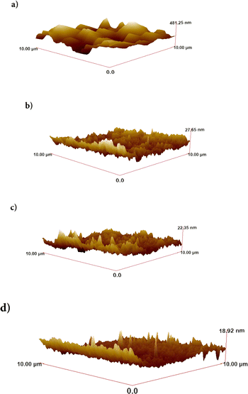 |
| | Fig. 1 AFM images of samples coated on quartz glasses in 10 × 10 μm2 scanning areas: (a) BaF2, (b) MgF2, (c) BaxMg1−xF2 (x > 0.5) and (d) BaxMg1−xF2 (x < 0.5). | |
The root mean square values (rms) of surface roughness, calculated from the surface images recorded with AFM, are associated with the homogeneous distribution of the morphological structure of the samples, and these values are as shown in Table 1.
Table 1 Root mean square (rms) values of surface roughness for BaF2 and MgF2 compounds and BaxMg1−xF2 alloys with different atomic concentrations
| Atomic concentration |
rms (nm) |
| BaF2 |
48.3 |
| MgF2 |
4.5 |
| BaxMg1−xF2 (barium-rich, x > 0.5) |
9.7 |
| BaxMg1−xF2 (magnesium-rich, x < 0.5) |
2.2 |
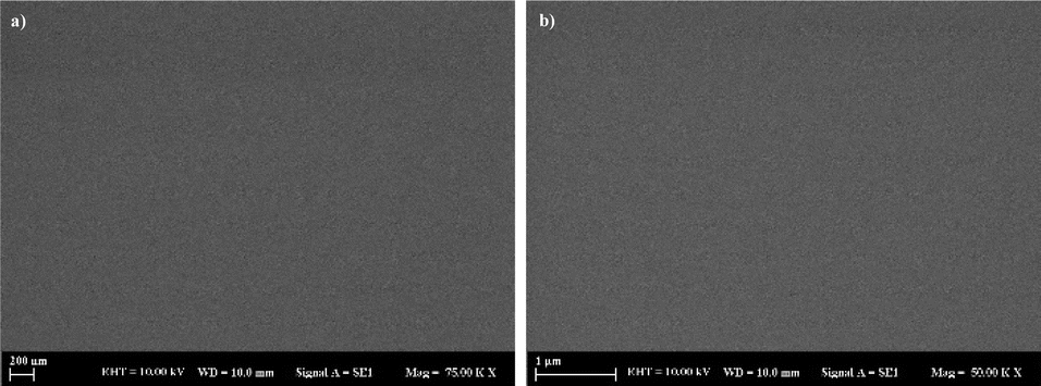
For each sample, the surface images monitored by SEM (scale bars: 200 nm and 1 μm) are shown in Fig. 2–5.
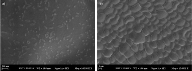 |
| | Fig. 2 Surface images of the BaF2 compound obtained by SEM, scale bars: (a) 200 nm, (b) 1 μm. | |
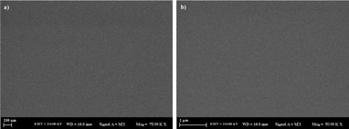 |
| | Fig. 3 Surface images of the MgF2 compound obtained by SEM, scale bars: (a) 200 nm, (b) 1 μm. | |
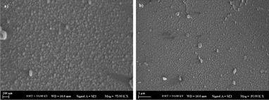 |
| | Fig. 4 Surface images of BaxMg1−xF2 (barium-rich, x > 0.5) alloy obtained by SEM, scale bars: (a) 200 nm, (b) 1 μm. | |
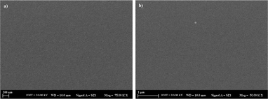 |
| | Fig. 5 Surface images of BaxMg1−xF2 (magnesium-rich, x < 0.5) alloy obtained by SEM, scale bars: (a) 200 nm, (b) 1 μm. | |
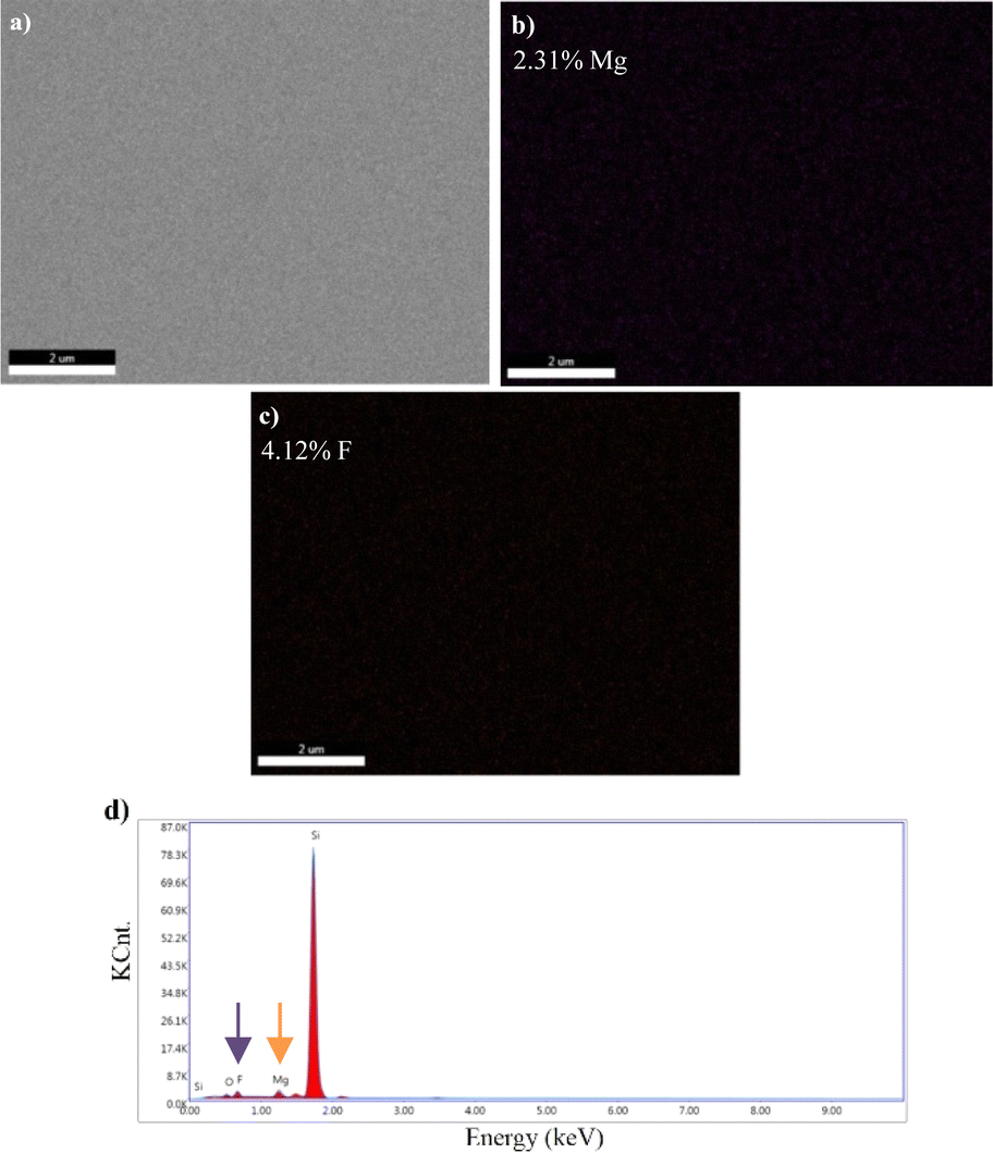
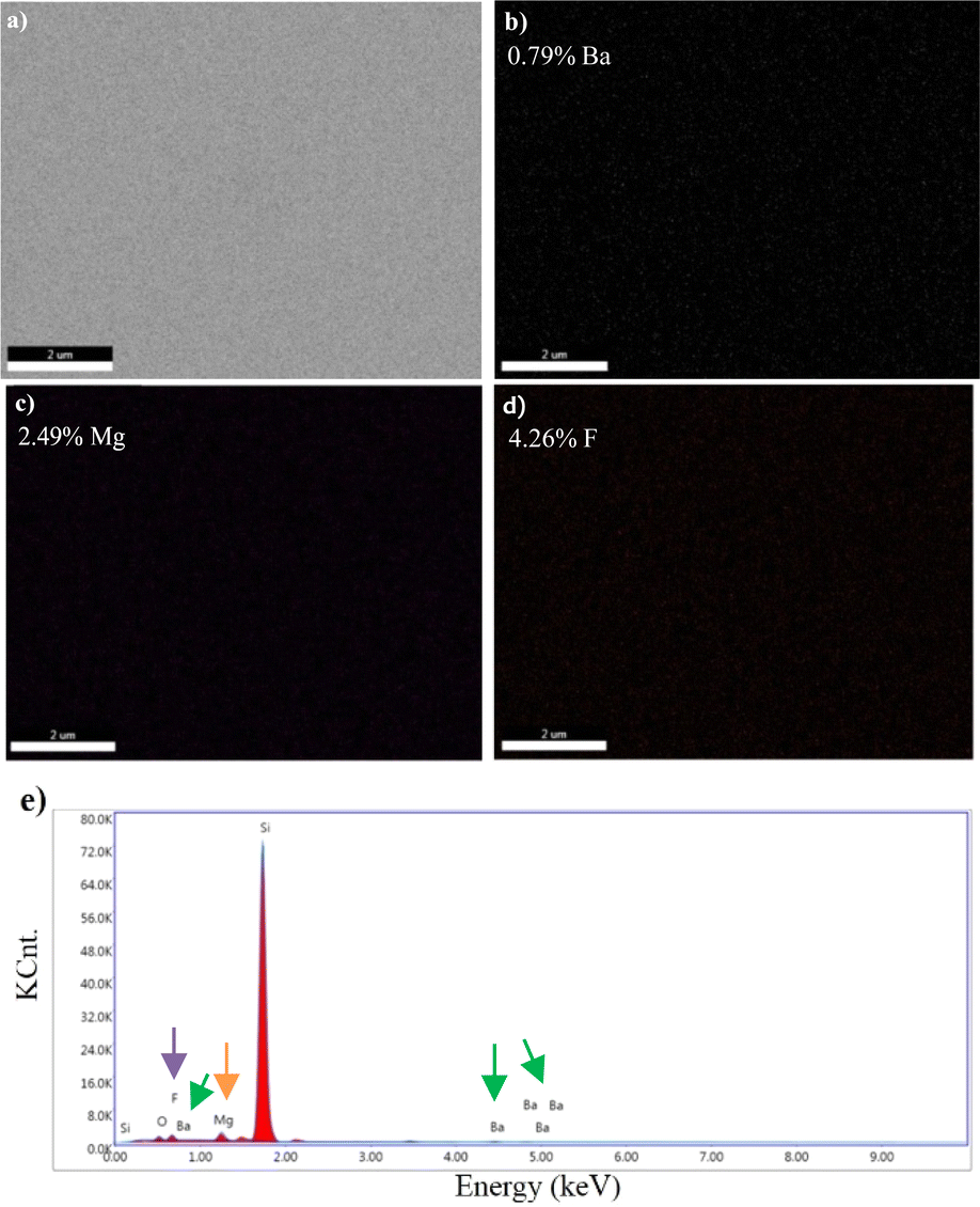
Images obtained by SEM-EDS, for the microstructural analysis of materials, are given in Fig. 6–9.
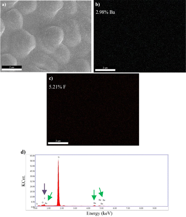 |
| | Fig. 6 SEM-EDS analysis results of 100 nm thick BaF2 compound. (a) SEM image of the surface topography, EDS mappings of (b) Ba, (c) F elements in BaF2 coating deposited on silicon substrate, (d) EDS spectrum of the area shown in (a) (scale bar is 2 μm). F element's and Ba element's EDS peaks are represented by purple and green arrows respectively. | |
 |
| | Fig. 7 SEM-EDS analysis results of 100 nm thick MgF2 compound. (a) SEM image of the surface topography, EDS mappings of (b) Mg, (c) F elements in MgF2 coating deposited on silicon substrate, (d) EDS spectrum of the area shown in (a) (scale bar is 2 μm). F element's and Mg element's EDS peaks are represented by purple and orange arrows respectively. | |
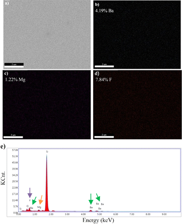 |
| | Fig. 8 SEM-EDS analysis results of 100 nm thick BaxMg1−xF2 (barium-rich, x > 0.5) alloy. (a) SEM image of the surface topography, EDS mappings of (b) Ba, (c) Mg, (d) F elements in BaxMg1−xF2 (barium rich, x > 0.5) coating deposited on silicon substrate, (e) EDS spectrum of the area shown in (a) (scale bar is 2 μm). F element's, Ba element's, and Mg element's EDS peaks are represented by purple, green, and orange arrows respectively. | |
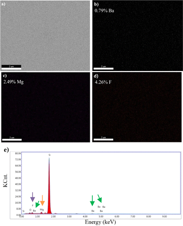 |
| | Fig. 9 SEM-EDS analysis results of 100 nm thick BaxMg1−xF2 (magnesium-rich, x < 0.5) alloy. (a) SEM image of the surface topography, EDS mappings of (b) Ba, (c) Mg, (d) F elements in BaxMg1−xF2 (magnesium-rich, x < 0.5) coating deposited on silicon substrate, (e) EDS spectrum of the area shown in (a) (scale bar is 2 μm). F element's, Ba element's, and Mg element's EDS peaks are represented by purple, green, and orange arrows respectively. | |
Fig. 10 shows the 2-dimensional surface acoustic images obtained by SAM, of the BaF2 and MgF2 compounds as well as the BaxMg1−xF2 alloys, coated on quartz glass.
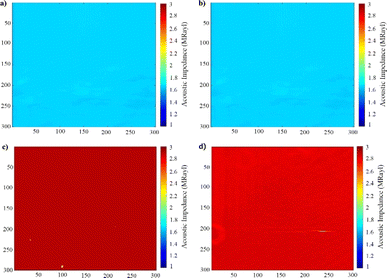 |
| | Fig. 10 Two-dimensional acoustic impedance maps of (a) BaF2 compound, (b) MgF2 compound, (c) BaxMg1−xF2 alloy (x > 0.5) and (d) BaxMg1−xF2 alloy (x < 0.5), recorded by 80 MHz SAM. The scanning area is 4.8 mm × 4.8 mm with 300 × 300 sampling points. The colour bar represents the variation in acoustic impedance values. | |
Table 2 displays acoustic impedance results. Mean acoustic impedance values are weighted averages, calculated from point values on five different surface areas of 0.3 mm × 0.3 mm on each sample.
Table 2 Surface acoustic impedance and standard deviation values of thin films, determined by SAM
| Sample |
Acoustic impedance (MRayl) |
Standard deviation (MRayl) |
| BaF2 |
1.655 |
0.016 |
| MgF2 |
1.679 |
0.010 |
| BaxMg1−xF2 (x > 0.5) |
2.910 |
0.028 |
| BaxMg1−xF2 (x < 0.5) |
2.835 |
0.021 |
3 Discussion
In order to perform morphological analysis, each sample surface was mapped with AFM and then with SEM. As can be seen in Fig. 1 samples have homogeneous morphological surface structure. The root mean square values (rms) of surface roughness, given in Table 1, are associated with the homogeneous distribution of the morphological structure of the samples.
Coating samples thinly with gold–palladium with Quorum-SC7620 device prior to the SEM imaging and measurement, reduced reflections on the sample surfaces, leading to the production of clearer surface images. The surface morphology images of the samples were obtained with the Zeiss EVO LS 10 device. All samples have highly homogeneous surfaces, as can be seen by analysing the surface images in Fig. 2–5 acquired by SEM, which determines surface homogeneity and average particle size for each element on the surface.
The surfaces have some defects that are in nanometer-scale. The Ba element's particle size is observed to be larger than that of Mg and F. The average particle sizes for Ba, Mg, and F were estimated from SEM surface images to be between 90 and 140 nm, 20 and 50 nm, and 40 and 80 nm, respectively.
SEM-EDS results demonstrated that B, Mg, and F were present in the structure of the materials coated with varying atomic concentrations (Fig. 6–9). In the EDS spectrum of the BaF2 compound (Fig. 6d), peaks were observed at 0.8 eV and 4.5 eV, confirming the presence of F and Ba, respectively. From the EDS maps, BaF2 has a stoichiometric ratio of Ba (2.98%) and F (5.21%). The presence of F and Mg was confirmed by peaks observed at 0.8 eV and 1.2 eV in the EDS spectrum of the MgF2 compound (Fig. 7d). EDS maps showed that MgF2 has a stoichiometric ratio of Mg (2.31%) and F (4.12%). The EDS spectrum of BaxMg1−xF2 (Barium rich, x > 0.5) alloy (Fig. 8e) showed peaks at 0.8 eV, 1.2 eV and 4.5 eV confirming the presence of F, Mg, and Ba, respectively. From the EDS maps, it was observed that BaxMg1−xF2 (barium rich, x > 0.5) had stoichiometric ratios of Ba (4.19%), Mg (1.22%) and F (7.84%). The presence of F, Mg, and Ba was confirmed by the EDS spectrum of the BaxMg1−xF2 (magnesium rich, x < 0.5) alloy (Fig. 9e), which displayed peaks at 0.8 eV, 1.2 eV, and 4.5 eV, respectively. From the EDS maps, it was observed that BaxMg1−xF2 (magnesium rich, x < 0.5) had stoichiometric ratios of Ba (0.79%), Mg (2.49%) and F (4.26%). In SAM, an 80 MHz frequency converter with a spot size of 17 μm and a focal length of 1.5 mm produces a 5 ns wide pulse with a repetition rate of 10 kHz, and acoustic waves reflected from the sample and reference are collected and analysed with the help of an oscilloscope. In this way, impedance and acoustic intensity maps of the region can be obtained with 300 × 300 sampling points in the 4.8 mm × 4.8 mm and 0.3 mm × 0.3 mm scanning areas with a lateral resolution of approximately 20 μm (Fig. 10). Acoustic signal reflections from the reference (distilled water) and sample surfaces were recorded using SAM in acoustic impedance mode to create surface acoustic images. In order to determine the weighted average acoustic impedance values, BaF2 and MgF2 compound and BaxMg1−xF2 alloy surface areas of 0.3 mm × 0.3 mm and 4.8 mm × 4.8 mm were analysed. Due to the different elasticity values of nanomaterials, and since elasticity of the materials effect the impedance values obtained by SAM, several defects are observed in the acoustic impedance maps with different acoustic impedance values as can be seen in Table 2.22 Reflections of acoustic waves from regions with many pores cause strong signals, and therefore, they are easily detected on SAM images (Fig. 10). These non-homogeneously distributed regions can be defined as surface defects of various shapes and sizes on thin-film coatings. The significant variations in the mean acoustic impedance values (Table 2) among the generated samples are worth mentioning. These changes also correspond to the changes in the micro-hardness and elasticity properties of the materials. Additionally, the low standard deviation values (Table 2) suggest that the prepared coatings have a relatively low surface defect rate.
4 Conclusions
Within the scope of this study, microstructure analysis of BaF2 and MgF2 compounds and BaxMg1−xF2 alloys (barium-rich and magnesium-rich) were determined using SEM-EDS technique, and surface morphology were determined using AFM, SEM and SAM techniques. The SEM-EDS analysis results demonstrate that pure compounds or alloys could be produced in a high vacuum environment. The materials produced had atomic concentrations that were found to be consistent with previous research based on elemental analysis. For surfaces of fabricated materials, EDS spectra display stoichiometric ratios. According to the EDS analysis results, the Ba and F elements are uniformly distributed on the material surface, and the atomic percentage ratio of Ba/F for the BaF2 compound is almost equal to 1/2. It is noted that the Mg and F elements are uniformly distributed on the material surface, and the atomic percentage ratio of Mg/F for the MgF2 compound is nearly equal to 1/2. In the BaxMg1−xF2 (barium-rich, x > 0.5) alloy, a stoichiometry has emerged that the ratio of the total atomic percentage value of Ba and Mg elements to the atomic percentage value of F is far away from 1/2. A stoichiometry has been identified for the BaxMg1−xF2 (magnesium-rich, x < 0.5) alloy, which shows that the ratio of the total atomic percentage value of the Ba and Mg elements to the atomic percentage value of the F elements is not very close to 1/2. The elements play a crucial role in the structure formation of the alloy surfaces produced in the vacuum environment. The surface morphology analysis of the materials revealed that, based on the roughness rms values derived from the three-dimensional AFM images with a scanning area of 10 × 10 μm2, BaF2 had the roughest structure and BaxMg1−xF2 (rich in magnesium, x < 0.5) had the smoothest structure. These findings suggest that MgF2 compound and BaxMg1−xF2 (magnesium rich) alloy structure can be used as buffer interface in multilayer structures in various optoelectronic applications such as thin film transistors, and light emitting diodes,23 while BaF2 structure or BaxMg1−xF2 (barium rich, x > 0.5) alloy can be used as an anti-reflective coating layer. Upon examination of the SEM analysis results, it was noted that every material surface displayed a very uniform morphology. We have come across tight structures with few intergranular spaces and few agglomerations. SAM was used to scan the material surfaces and observe how the atomic concentration affected the material's surface. It is known that the acoustic impedance value changes with material's elasticity. Because surface hardness and elasticity are crucial for acoustic devices, BaxMg1−xF2 thin film alloy materials with high acoustic impedance values can be employed in these devices, according to the results obtained in this study using the SAM method.
5 Material and methods
5.1 Samples
BaF2 and MgF2 compounds' and BaxMg1−xF2 alloys' coatings at different atomic concentrations were deposited on (100)-oriented, n-type silicon (n-Si) and quartz glass substrates using 99% pure BaF2 and MgF2 targets in rf magnetron sputtering setup. At the forefront of surface coating technology are physical vapour deposition techniques, of which rf magnetron sputtering is the most often used method. The frequency used in this technique is mainly 13.56 MHz. In this study, the compounds and alloys were coated on quartz glass and Si substrates using the Nanovak NVTS – 500 rf magnetron sputtering system. Under the same vacuum environment and conditions, the substrates to be coated were set up. Thus, homogeneous coatings of 100 ± 10 nm thickness were achieved for all substrates under identical conditions by the rotating electrode. BaF2 and MgF2 compound nanomaterials were deposited by placing high purity (99.9%) BaF2 target and high purity (99.9%) MgF2 target in rf vacuum system, respectively. BaF2 and MgF2 targets were employed in the same vacuum system using a co-sputtering technique to produce BaxMg1−xF2 alloys. The coatings were carried out in an atmosphere of 2 Pa Ar gas and at a rotational speed of 5 rpm. Substrates were kept at room temperature. Among the deposition parameters in the vacuum chamber, the base pressure is in the range of 10−4 Pa, and the deposition rate is in the range of 0.03–0.06 Å s−1. Deposition times and powers were adjusted in the vacuum chamber so that the thickness of the materials was ∼100 nm. With various spectroscopic and microscopic techniques, it was possible to determine how the atomic concentration parameter affected the material's morphological characteristics. For each spectroscopic and microscopic techniques, two different BaxMg1−xF2 alloys were used: Barium rich alloy, x > 0.5 and magnesium rich alloy, x < 0.5.
5.2 Atomic force microscopy
In this study, surface characterization of BaxMg1−xF2 thin film materials with different atomic concentrations was performed with a high-performance non-contact mode AFM (NanoMagnetics Instruments LTD, Oxford, UK) through a scanning area of 10 × 10 μm2. The characterization is performed at room temperature conditions, the average radius of the tip was ∼200 Å, and the scan speed was taken as 5 μm s−1. The two-dimensional surface images acquired from the measurements were used to compute surface roughness values (rms).
5.3 Scanning electron microscopy and energy dispersive X-ray spectroscopy
The surface images of BaF2 and MgF2 compounds and BaxMg1−xF2 alloy samples were performed with SEM (Zeiss EVO LS 10), which provides high-resolution magnification for the determination of the cracks/fractures and morphological structure of the materials and allows analysis by taking images in this way. For SEM imaging, the samples were thinly coated with gold–palladium within 90 seconds at a voltage of 10 mV in a vacuum environment of roughly 1 Pa. This procedure was carried out in a vacuum setting using a Quorum-SC7620 device prior to the measurement for obtaining clearer images. Additionally, the energy-dispersive X-ray spectroscopy (ESEM-EDS) technique, which is crucial for material identification and quantitative analysis, was utilized to characterize the samples' structural properties.
5.4 Scanning acoustic microscopy
Utilizing SAM (Honda Electronics SAM AMS-50SI), which uses ultrasound signals to create visual images of the variations in the mechanical properties of the samples and allows non-destructive acquisition of images of structures that are difficult to be observed with other techniques by using the ability of acoustic waves to penetrate optically opaque materials, the surface images of BaF2 and MgF2 compounds and BaxMg1−xF2 alloys coated on quartz glass substrates were determined within about two minutes for each sample.24 Our earlier research provides comprehensive details on this method and the experimental setup.22,25–27
Data availability
The presented data is available upon request.
Author contributions
F. G. did the conceptualization. E. B., B. T. and F. G. conducted the experiments, and analysed the results. B. T. and F. G. wrote the original draft of the manuscript. B. D. and B. T. edited the manuscript. All authors reviewed the manuscript.
Conflicts of interest
There are no conflicts to declare.
Acknowledgements
Scanning acoustic microscopy studies were supported by a grant from the Ministry of Development of Turkey (Project Number: 2009K120520).
Notes and references
- I. I. Ebralidze, N. O. Laschuk, J. Poisson and O. V. Zenkina, Colorimetric Sensors and Sensor Arrays, Springer, Amsterdam, The Netherlands, 1st edn, 2019 Search PubMed.
- I. Constantinoiu and C. Viespe, Sensors, 2020, 20, 5118 CrossRef CAS PubMed.
- A. Palla-Papavlu, S. I. Voicu and M. Dinescu, Chemosensors, 2021, 9, 105 CrossRef CAS.
- R. Liu, X. Li, X. Hu and H. Dong, Surf. Coat. Technol., 2013, 232, 906–911 CrossRef CAS.
- Q. Wang, F. Zhou, C. Wang, M. F. Yuen, M. Wang, T. Qian, M. Matsumoto and J. Yan, Mater. Chem. Phys., 2015, 158, 74–81 CrossRef CAS.
- S. Hou, Surf. Eng., 2016, 32, 745–749 CrossRef CAS.
- D. D. Kumar, G. S. Kaliaraj, A. M. K. Kirubaharan, K. Alagarsamy, V. Vishwakarma and R. Baskaran, Surf. Coat. Technol., 2019, 374, 569–578 CrossRef CAS.
- S. Hou, W. Yu, Z. Yang, Y. L. adn L. Yang and S. Lang, Coatings, 2020, 10, 999 CrossRef CAS.
- G. S. Kaliaraj, S. Thukkaram, K. Alagarsamy, A. M. K. Kirubaharan, L. K. Paul, L. Abraham, V. Vishwakarma and S. Sagadevan, Surf. Interfaces, 2021, 24, 101086 CrossRef CAS.
- S. Nastyshyn, Y. Stetsyshyn, J. Raczkowska, Y. Nastishin, Y. Melnyk, Y. Panchenko and A. Budkowski, Polymers, 2022, 14, 4245 CrossRef CAS.
- G. A. M. K. Vishwakarma and V. Kaliaraj, Coatings, 2023, 13, 69 CrossRef.
- M. Friz and F. Waibel, Optical Interference Coatings, Elsevier, Berlin, Heidelberg, 1st edn, 2003 Search PubMed.
- S. Vyas, Johnson Matthey Technol. Rev., 2020, 64, 202–218 CrossRef CAS.
- S. Oktik and I. Sokmen, Thin-Film Technologies for Glass Surfaces, Wiley Online Library, 2023 Search PubMed.
- V. Tkachenko, I. Maksimchuk, V. Shklover, G. Katrich and V. Klimov, Appl. Phys. A: Mater. Sci. Process., 1996, 62, 285–287 CrossRef.
- Q. Zheng, X. Wang and D. Thompson, Opt. Mater. Express, 2023, 13, 2380–2391 CrossRef CAS.
- E. N. Kotlikov and A. Y. Novikova, Opt. Spectrosc., 2014, 17, 381–385 CrossRef.
- E. Kotlikov, E. Khonineva and V. Prokashev, J. Opt. Technol., 2004, 71, 407–410 CrossRef CAS.
- L. V. Rodríguez-de Marcos, J. I. Larruquert, J. A. Méndez and J. A. Aznárez, Opt. Mater. Express, 2017, 7, 989–1006 CrossRef.
- A. Karvounis, F. Timpu, V. V. Vogler-Neuling, R. Savo and R. Grange, Adv. Opt. Mater., 2020, 8, 2001249 CrossRef CAS.
- M. Sakthivel, S. S. Mary, V. Balasubramani, A. Ibrahim, J. Hakami and V. R. M. Reddy, Inorg. Chem. Commun., 2022, 141, 109511 CrossRef CAS.
- F. Guzelcimen, B. Tanoren, C. Cetinkaya, K. M. Donmez, H. I. Efkere, Y. Ozen, D. Bingol, M. Sirkeci, B. Kinaci, M. Unlu and S. Ozcelik, Radiat. Oncol., 2020, 15, 38 CrossRef.
- C. S. Wan, J. Bullock, T. Allen, M. Hettick, D. Yan, P. Zheng, X. Zhang, J. Cui and J. McKeon, et al., ACS Appl. Mater. Interfaces, 2016, 8, 14671–14677 CrossRef PubMed.
- Y. Y. Yang, Y. S. Jin and S. Y. Luo, Surf. Coat. Technol., 1997, 91, 95–100 CrossRef CAS.
- B. Bilen, B. Gökbulut, U. Kafa, E. Heves, M. N. Inci and M. B. Unlu, Sci. Rep., 2018, 8, 14378 CrossRef.
- B. Bilen, L. T. Sener, I. Albeniz, M. Sezen, M. B. Unlu and M. Ugurlucan, Sci. Rep., 2019, 9, 1–10 CrossRef CAS PubMed.
- I. Demirkan, G. Yaprak, C. Ceylan, E. Algul, M. Parlak, C. O. Tomruk, B. Bilen and M. B. Unlu, Radiat. Oncol., 2020, 15, 38 CrossRef PubMed.
|
| This journal is © The Royal Society of Chemistry 2024 |
Click here to see how this site uses Cookies. View our privacy policy here. 
 Open Access Article
 This Open Access Article is licensed under a Creative Commons Attribution-Non Commercial 3.0 Unported Licence
 *b,
Beste Dipcin
*b,
Beste Dipcin