 Open Access Article
Unlocking the effect of film thickness on the thermoelectric properties of thermally evaporated Cu2−xSe thin films
Muhammad Irfan a,
Sajid Butt
 *a,
Sumayyab,
Muhammad Waseem Akram
 a,
Muhammad Saadullaha,
Muhammad Abdul Basit
 b,
Jahanzeb Ahmadb,
Muhammad Yasira and
Huma Ozaira
aDepartment of Space Science, Institute of Space Technology, Islamabad 44000, Pakistan. E-mail: sajid.butt@ist.edu.pk
bDepartment of Material Science & Engineering, Institute of Space Technology, Islamabad 44000, Pakistan
First published on 25th November 2024
Abstract
Miniaturization is crucial to realize thermoelectric (TE) devices as an energy source for smart utilities. The present work reports the bulk-like ZT value realized in Cu2−xSe thin films in the mid-temperature range. The effect of varying the film thickness on the structural and TE properties were systematically studied, and the obtained results were compared with that of their bulk counterpart. The detailed structural characterizations revealed the nonstoichiometric polycrystalline nature of Cu2−xSe with the unusual presence of monoclinic and cubic phases. Upon increasing the film thickness, the TE measurements showed a simultaneous increase in the electrical conductivity (σ) and Seebeck coefficient (S) due to increased grain size and uniformity. Due to the simultaneous increase in σ and S, an ultrahigh power factor (PF) value of 5185 μW m−1 K−2 and a bulk-like figure of merit ZT ≈ 1.2 were achieved.
1. Introduction
Global population growth has prompted an increased need for renewable energy resources without the emission of toxic gases that destroy our ecosystem.1,2 Energy conversion via thermoelectric materials is an advanced technology for the recovery of waste heat into useful electricity and cooling applications.3,4 Thermoelectric devices have several advantages because unlike conventional generators, the heat can be converted directly into electricity without any moving parts and solid-state refrigeration.5,6 The performance of any thermoelectric material is evaluated by a dimensionless figure of merit: , where S is the Seebeck coefficient, σ is the electrical conductivity, κ is the thermal conductivity, and T is the absolute temperature. A material with high thermoelectric efficiency possesses high electrical conductivity, a high Seebeck coefficient and a low thermal conductivity. But it is quite challenging to enhance the figure of merit ZT because these three parameters are interlinked with each other and have an interplaying nature. In recent decades, plenty of work has been done to improve the ZT value by controlling the electron and phonon transport through nanostructuring.7,8 Nanostructuring can simultaneously increase σ and S and reduce κ through the energy filtering or quantum confinement effects.9–11
Copper selenide (Cu2Se) is a binary compound having a complex crystal structure due to the superionic behavior of Cu ions into the lattice of Cu2Se.12 Furthermore, Cu2−xSe undergoes a crystallographic phase transition at approximately 400 K. Recently, Cu2Se has been extensively studied due to its phonon-liquid electron-crystal (PLEC)-like behavior.13–15 Cu2Se exhibits high electrical conductivity, low thermal conductivity and moderate Seebeck coefficient. According to the literature, a high ZT value of 1.5 was observed at 1000 K for Cu2Se that was synthesized by melting, followed by spark plasma sintering (SPS).16 A higher ZT value of 1.9 was achieved at 873 K for Cu2Se by doping Te at the selenium site.17 Further improvement of ZT up to 2.0 at 1000 K was realized by the S-doped Cu2Se.18 So far, the highest ZT value of 2.62 at 1029 K has been reached for the Al-doped Cu2Se bulk.19 The flexible thin films of Cu2Se that were deposited via co-evaporation reached a ZT value of 0.35.20 A slightly improved ZT of 0.4 was achieved when the films were deposited by pulsed hybrid reactive magnetron sputtering (PHRMS).21 The highest reported ZT value of 0.58 for Cu2Se was achieved through pulsed laser deposition (PLD).22 Although the bulk Cu2Se have higher TE performance as compared to the thin films, the thin films have their own applications and advantages over the bulk material. The thin films of Cu2Se offer several advantages related to the miniaturization of devices, and also reduce the material costs. A variety of Cu2−xSe film deposition techniques have been reported, including the hydrothermal method, galvanic synthesis, solution growth, chemical bath deposition, and electrochemical deposition.23–30
Herein, we present the improved thermoelectric performance of thermally evaporated Cu2−xSe thin films having various thicknesses. As compared to other thin film deposition methods, vacuum thermal evaporation offers several advantages such as uniform film thickness, good compaction and adhesion to the glass substrate, and a commonly available technique. The detailed structural characterizations unveil the dependence of the improved TE performance over the Cu2−xSe film thickness.
2. Materials and methods
Polycrystalline Cu2−xSe powdered samples were prepared through solid state reaction of elemental Cu and Se powders, and the detailed method has been discussed elsewhere.12 Cu2−xSe films of various thicknesses were deposited over glass through thermal evaporation method using NANOVAK 3000TH. The glass substrates were thoroughly cleaned using a sequential cleaning process involving the use of a detergent, ethanol and acetone, followed by drying with hot air before mounting the substrate into the evaporation unit. Cu2−xSe pellets were loaded into the tungsten boat. The lid of the evaporation unit was closed, and a pressure of 1.33 × 10⁻⁶ mbar was maintained before evaporation. A deposition rate of 0.5 Å s−1 and a sample rotation speed of 20 rpm were set for the deposition. The film thickness was controlled by a quartz crystal sensor (INFICON's). Films with thicknesses of 50 nm, 100 nm, 300 nm and 500 nm were obtained. The as-deposited films were annealed in a vacuum furnace at 400 °C for 1 h at a pressure of 1.5 × 10⁻¹ mbar.X-ray diffraction (XRD) patterns of the powder and films were recorded by a BRUKER diffractometer (D2 PHASER) using Cu-Kα radiation. X-ray photoelectron spectroscopy (XPS) of the powder sample was performed using monochromatic Al Kα radiation with Thermo Scientific Escalab-250xi to obtain the elemental composition and chemical states of Cu and Se. The charging effect was normalized with reference to C 1s (284.8 eV). The high-resolution Cu and Se core level spectra were analyzed after the subtraction of backgrounds using the Shirley algorithm with XPS PEAK41 software. The surface morphology and chemical composition of the samples were measured using scanning electron microscopy (SEM) (MIRA3 TESCAN) coupled with an energy dispersive X-ray (EDX) detector (X-MaxN). The particle size was estimated from SEM micrographs using ImageJ software. The electrical conductivity and Seebeck coefficient were measured utilizing the well-known four-probe method over the temperature range of 298–575 K by the thermoelectric parameter test system (Joule Yacht-NAMICRO-3L). The temperature-dependent carrier's concentration (n) and mobility (μ) were determined by the Hall measurement system (ECOPIA HMS 5000).
3. Results and discussion
The room temperature X-ray diffraction (XRD) patterns of the powdered, 100 nm, and 500 nm thin film samples are shown in Fig. 1. The powder and thin film samples exhibit the Cu2−xSe phase, demonstrating polymorphism with the predominant presence of the monoclinic phase indexed by JCPDF#27-1131 and a minor presence of the cubic phase indexed by JCPDF#06-0680. The diffraction peaks of all samples indicate good crystallinity. The XRD pattern for the 100 nm sample displays a phase composition that is similar to that of the powder and 500 nm film, but with reduced intensity, which could be attributed to its lower crystallinity compared to the bulk and thicker film sample. The lattice parameter and crystallite size were calculated using MDI Jade software to analyze the impact of the film thickness on the structural properties, as presented in Table 1. The results indicate a decrease in the crystallite size and an increase in the lattice parameters with decreasing film thickness. This expansion of the lattice parameters and reduction in the crystallite size in thinner films are likely due to the presence of more pronounced Cu vacancies.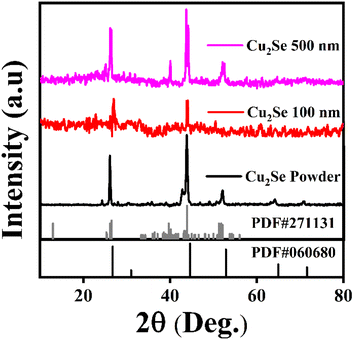 | ||
| Fig. 1 Room temperature XRD patterns of the Cu2Se powder (as-prepared) and thin film having thicknesses of 100 and 500 nm evaporated over a glass substrate. | ||
| Sample | Lattice parameter (Å) | Crystallite size (Å) |
|---|---|---|
| Cu2Se powder | 8.2863 | 454 |
| Cu2Se 500 nm | 9.2136 | 282 |
| Cu2Se 100 nm | 10.6088 | 88 |
The deconvoluted Cu 2p and Se 3d high-resolution X-ray photoelectron spectroscopy (XPS) spectra are shown in Fig. 2(a and b). For Cu 2p, the synthetic peaks at binding energies of 932.2 eV (Cu 2p3/2) and 952.2 eV (Cu1/2) correspond to Cu1+ attached to Se, and the peaks at 933.5 eV (Cu 2p3/2) and 953.5 eV (Cu 2p1/2) correspond to Cu2+ attached to Se, as shown in Fig. 2(a). The peaks appearing at higher binding energies of 935.4 eV (Cu 2p3/2) and 955.1 eV (Cu 2p1/2) are attributed to the (Cu)–O bond, indicating that the surface is oxidized. The satellite peaks also indicate the presence of the Cu–O bond. The deconvoluted spectrum of Se 3d is shown in Fig. 2(b). Due to the small spin–orbit-splitting value (∼0.86 eV) of Se 3d electrons, it is difficult to assign absolute binding energy values to the synthetic peaks under Se 3d5/2 and Se 3d3/2.31 However, a careful analysis reveals the presence of Se2− attached to Cu1+ and Cu2+, as shown in Fig. 2(b).
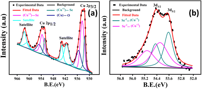 | ||
| Fig. 2 High-resolution X-ray photoelectron spectroscopy (XPS) spectrum of Cu 2p (a) and Se 3d (b) of the Cu2Se powder. | ||
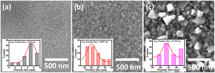
The surface morphological images of the Cu2−xSe thin films of 50 nm, 100 nm and 500 nm thicknesses taken using secondary electron (SE) are shown in Fig. 3. The SE images of the 50 nm and 500 nm-thickness films, as shown in Fig. 3(a) and (c), respectively, reveal the morphological difference between the thin films prepared with different thicknesses. As the film thickness increased to 100 nm, the grain size improved. Furthermore, the films became denser and more uniform, although still less so than the 500 nm sample. The films with small thickness (50 nm) resulted in non-uniform films with high porosity, smaller grain size, and poor grain alignment. Meanwhile, upon increasing the film thickness, the films were found to be more uniform and densely packed, with a larger grain size and well-aligned grains. Moreover, the particle size in the inset of Fig. 3 showed an increasing trend with increasing thickness. This trend is responsible for the better grain alignments in thicker films, which is consistent with the crystallite size results from XRD.
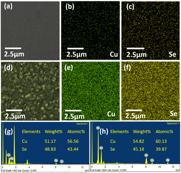
The percentage compositions of the 100 nm and 500 nm Cu2−xSe were evaluated by EDS, as given in Fig. 4, demonstrating the exclusive presence of copper (Cu) and selenium (Se). The inset table in Fig. 4(g and h) shows the atomic and weight percentages of the Cu and Se atoms. These results infer that the evaporated sample is Cu deficient, which results in an increased conductivity compared to that of the stoichiometric Cu2Se.32 This observation is further supported by the Cu![[thin space (1/6-em)]](https://www.rsc.org/images/entities/char_2009.gif) :
:![[thin space (1/6-em)]](https://www.rsc.org/images/entities/char_2009.gif) Se ratios of 1.508
Se ratios of 1.508![[thin space (1/6-em)]](https://www.rsc.org/images/entities/char_2009.gif) :
:![[thin space (1/6-em)]](https://www.rsc.org/images/entities/char_2009.gif) 1 and 1.302
1 and 1.302![[thin space (1/6-em)]](https://www.rsc.org/images/entities/char_2009.gif) :
:![[thin space (1/6-em)]](https://www.rsc.org/images/entities/char_2009.gif) 1 for the 500 nm and 100 nm samples, respectively. These values confirm the presence of the Cu deficiencies, with the thinner film being more Cu deficient, as suggested by XRD data. Elemental mapping for both samples, shown in Fig. 4(b, c, e, and f), illustrates that copper and selenium are homogeneously distributed across the films. Furthermore, the Cu mapping for the 100 nm sample indicates a lower Cu concentration as compared to the 500 nm sample, reflecting the thinner film being more Cu deficient.
1 for the 500 nm and 100 nm samples, respectively. These values confirm the presence of the Cu deficiencies, with the thinner film being more Cu deficient, as suggested by XRD data. Elemental mapping for both samples, shown in Fig. 4(b, c, e, and f), illustrates that copper and selenium are homogeneously distributed across the films. Furthermore, the Cu mapping for the 100 nm sample indicates a lower Cu concentration as compared to the 500 nm sample, reflecting the thinner film being more Cu deficient.
The temperature-dependent electrical conductivity (σ), Seebeck coefficient (S), power factor (PF), and electronic thermal conductivity (ke) were measured, while the lattice thermal conductivity (kL), total thermal conductivity (k), and figure of merit (ZT) were estimated for all of the series of films in the range of 298 K to 575 K.
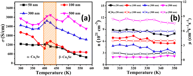
The temperature-dependent electrical conductivity of all the films is shown in Fig. 5(a). The electrical conductivity decreases with increasing temperature for all of the films, which is similar to the behavior of highly degenerate semiconductors. This behavior is consistent with the typical temperature dependence of the electrical conductivity of Cu2−xSe films, as reported previously.33 A phase transition from α-Cu2Se to high-temperature β-Cu2Se phase can be observed within the temperature range of 400 K to 450 K. There was a noticeable increase in electrical conductivity during the phase change. However, after 450 K, the electrical conductivity decreased for the β-phase, which is also in good agreement with previous reports.34 Conversely, an increase in the film thickness results in increased electrical conductivity, showing a maximum value for the 500 nm thin film. The reason behind the high electrical conductivity for all the series compared to its bulk counterparts12 can be attributed to the increased film uniformity and improved grain alignment as revealed by SEM results in Fig. 3, which resulted in the enhanced mean free path of the charge carriers as inferred from the carriers' mobility (μ500 nm > μ50 nm), given in Fig. 5(b). Additionally, the Cu deficiencies, confirmed by the EDS data in Fig. 4, enhance n and contribute to the increased electrical conductivity of all films.32 However, the lower electrical conductivity in thinner films is due to reduced μ, caused by the presence of more Cu vacancies, that act as carrier scattering sites. These vacancies hinder the movement of the charge carriers, resulting in decreased electrical conductivity.
Fig. 5(b) illustrates the temperature-dependent Hall measurements for all samples, showing that n decreases while μ increases with increasing film thickness. The observed decrease in n with thicker films is likely due to a reduction in the Cu deficiencies, as confirmed by the EDS data in Fig. 4. Thinner films exhibit higher Cu deficiencies, leading to greater carrier concentration values, whereas thicker films, with fewer Cu vacancies, show reduced carrier concentration.32 Conversely, the increase in μ with film thickness can be attributed to a reduction in the grain boundary scattering, which is more significant in thinner films. In these thinner films, a decrease in the crystallite size, as indicated by XRD data, introduces more grain boundaries along with higher Cu deficiencies, contributing to increased carrier scattering in the Cu2−xSe lattice and thus lowering μ. SEM images show that thinner films are more porous with smaller grains, resulting in more frequent grain boundary scattering events that limit μ. In contrast, thicker films have larger, better-aligned grains and fewer grain boundaries, allowing for enhanced μ. This improved μ in the thicker films ultimately contributes to an increase in the overall electrical conductivity.32,35
The temperature-dependent Seebeck coefficient has shown an increasing trend with increasing temperature, as displayed in Fig. 6(a). A positive Seebeck coefficient has been observed throughout the temperature range, which demonstrates that the holes are the majority charge carriers. According to the literature, the reason associated with this increment in the Seebeck coefficient with increasing temperature is attributed to the direct relation with temperature and inverse relation with n.36 However, an anomalous behavior at higher temperatures is observed in the Seebeck coefficient. This anomaly could be attributed to possible phase transitions within the Cu2−xSe phase or changes in the Cu deficiency levels at elevated temperatures, which influence the n. Furthermore, increased phonon scattering at higher temperatures may also play a role in this behavior.37,38 The Seebeck coefficient of all the series of Cu2−xSe thin films has shown an increasing trend with increasing film thickness due to decreased n with increasing film thickness (n500 nm < n50 nm), as confirmed by the Hall measurements given in Fig. 5(b). Fig. 5(b) shows that the n decreases with increasing film thickness. This is associated with more Cu deficiencies in thinner films, which can be confirmed by the EDX data in Fig. 4. The decrease in n with increasing thickness results in an increase of the Seebeck coefficient at higher thicknesses.12,39
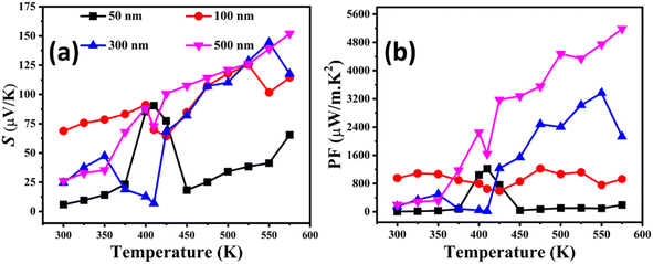 | ||
| Fig. 6 Temperature-dependent Seebeck coefficient (S) (a) and the power factor (PF) (b) of the entire series of Cu2−xSe thin films having thicknesses of 50 nm, 100 nm, 300 nm and 500 nm. | ||
Fig. 6(b) depicts the temperature dependence of the power factor (PF = S2σ) of all the Cu2−xSe thin films of various thicknesses. The simultaneous increase in electrical conductivity and Seebeck coefficient for all the series results in an increased PF value. The maximum value of the power factor of 5185 μW m−1 K−2 at 575 K has been achieved for the 500 nm Cu2−xSe film, which is about 91% larger than that of its bulk counterpart and 99% larger than that of the previously reported thin films at the same temperature.12 To the best of our knowledge, this is the highest reported power factor for Cu2−xSe thin films so far, which is due to the synergy of the simultaneous improvement in n and μ.
It is difficult to measure the total thermal conductivity of thin films. The availability of the specialized equipment is also an issue. To address the issue, we calculated the total (k) by adding the electronic thermal conductivity (ke) and lattice thermal conductivity (kL). ke can be calculated through the Wiedemann Franz Law (ke = LσT), where L, σ and T are the Lorentz number, electrical conductivity and temperature, respectively. A constant value of L, i.e., 2.05 × 10−8,40 has been used to calculate ke, as shown in Fig. 7(a). According to the literature,39 the k value of Cu2−xSe is largely influenced by the ke part due to the superionic nature of copper selenide. For simplicity, the kL values were estimated to be the same as that of the bulk counterpart of Cu2Se from our previous study,12 as shown in the inset of Fig. 7(a). However, we recognize that the kL in thin films is typically much lower than that in bulk materials due to the increased phonon scattering at the interfaces and surfaces in thin films. This enhanced scattering reduces the effective thermal conductivity in thin films compared to bulk counterparts. Therefore, the actual kL in our thin films is expected to be lower than the bulk value used, which could lead to an overestimation of the total thermal conductivity (k).37 Despite this, the trends observed in the thermal conductivity remain consistent with expectations, as the contribution of the ke dominates at higher thicknesses.
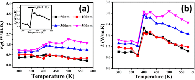 | ||
| Fig. 7 Temperature-dependent electronic thermal conductivity (ke) having a lattice thermal conductivity (kL) in the inset12 (a) and the total thermal conductivity (k) (b) of the entire series of Cu2−xSe thin films having thicknesses of 50 nm, 100 nm, 300 nm and 500 nm. | ||
Fig. 8 presents the temperature-dependent ZT for the entire series of samples of Cu2−xSe thin films. The increase in ZT values increased with increasing film thickness due to increased PF. The highest ZT value of 1.2 at 575 K has been achieved for the 500 nm thick sample, which is about 10× greater than that of the 50 nm sample and 51% greater than that of the reported value for thin films at the same temperature.22 The achieved ZT value is comparable to the bulk value reported in the literature, and largest among the previously reported data for thin films.22 According to the literature, different techniques have resulted in different values for ZT. A. Wang et al. reported an estimated ZT ≈ 0.58 through pulsed laser deposition technique.22 Conversely, J. A. Perez-Taborda et al. reported an estimated ZT ≈ 0.4 at room temperature through pulsed hybrid reactive magnetron sputtering (PHRMS),21 while M. R. Scimeca et al. reported a value of ZT ≈ 0.34 by the solution processing route41 for Cu2Se thin films. The estimated ZT values of the current Cu2−xSe films may still be empirically underestimated because the k values used here are overestimated. Thus, the actual ZT value may even be higher than 1.2 at 575 K for the 500 nm thick sample. The proposed strategy suggests that the phonon-liquid and electron-crystal (PLEC) behavior of Cu2Se could further be elaborated by decoupling electronic and thermal transportation through nanostructuring.
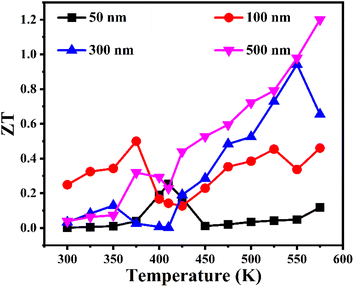 | ||
| Fig. 8 Temperature-dependent figure of merit ZT of the entire series of Cu2−xSe thin films having thicknesses of 50 nm, 100 nm, 300 nm and 500 nm. | ||
4. Conclusion
A facile method for the improved thermoelectric (TE) performance of the Cu2−xSe films has been reported, and a thorough investigation over structure-property linkage has been developed. Cu2−xSe thin films with various thicknesses have been successfully deposited on a glass substrate via thermal evaporation technique. Deposition of crystalline, compact and densely packed Cu2−xSe thin films without disturbing their stoichiometry has always been a challenge. As the thickness of the films increases, the grain size and stoichiometric ratio change, resulting in a significant effect on the n, which influences the electrical conductivity and Seebeck coefficient. An ultrahigh power factor has been achieved due to the synergetic effects, which simultaneously improve the electrical conductivity and Seebeck coefficient. As a result, the figure of merit (ZT) value of 1.2 in the mid-temperature range has been achieved, which is highest among all the previously reported work. Our research outcomes suggest that manipulating the film thickness holds great potential for tuning and optimizing the thermoelectric properties of Cu2−xSe.Data availability
Data are available upon request from the authors.Author contributions
Muhammad Irfan: conceptualization, investigation research methodology, experimentation and characterization, drafting and analyzing data, and writing. Sajid Butt: supervision, funding acquisition, validation, sources, reviewing and editing. Summaya: investigation, reviewing and editing. Muhammad Waseem Akram: reviewing and editing. Muhammad Saadullah: reviewing and editing. Muhammad Abdul Basit: reviewing and editing. Jahanzeb Ahmed: sources. Muhammad Yasir: sources. Huma Ozair: reviewing and editing.Conflicts of interest
All authors declare that there are no conflicts of interest.Acknowledgements
All authors are thankful to the Higher Education Commission (HEC) of Pakistan for financial support through the 8096/NRPU/R&D/HEC/2017 project.References
- I. Dincer, Renewable energy and sustainable development: a crucial review, Renewable Sustainable Energy Rev., 2000, 4, 157–175, DOI:10.1016/S1364-0321(99)00011-8.
- H. Mamur and R. Ahıska, A review: thermoelectric generators in renewable energy, Int. J. Renew. Energy Res., 2014, 4, 128–136 Search PubMed.
- D. M. Rowe, Thermoelectrics Handbook Macro to Nano, 2005, vol. 80, pp. 215–230 Search PubMed.
- L. E. Bell, Cooling, heating, generating power, and recovering waste heat with thermoelectric systems, Science, 2008, 321, 1457–1461, DOI:10.1126/science.1158899.
- J. R. Sootsman, D. Y. Chung and M. G. Kanatzidis, New and old concepts in thermoelectric materials, Angew. Chem., Int. Ed., 2009, 48, 8616–8639, DOI:10.1002/anie.200900598.
- M. Zebarjadi, K. Esfarjani, M. S. Dresselhaus, Z. F. Ren and G. Chen, Perspectives on thermoelectrics: from fundamentals to device applications, Energy Environ. Sci., 2012, 5, 5147–5162, 10.1039/c1ee02497c.
- L. D. Hicks and M. S. Dresselhaus, Effect of quantum-well structures on the thermoelectric figure of merit, Phys. Rev. B:Condens. Matter Mater. Phys., 1993, 47, 12727–12731, DOI:10.1103/PhysRevB.47.12727.
- Y. Wang and H. J. Fan, Improved Thermoelectric Properties of La1−xSrxCoO3 Nanowires, J. Phys. Chem. C, 2010, 114, 13947–13953, DOI:10.1021/jp105367r.
- H. Yang, J. H. Bahk, T. Day, A. M. S. Mohammed, G. J. Snyder, A. Shakouri and Y. Wu, Enhanced thermoelectric properties in bulk nanowire heterostructure-based nanocomposites through minority carrier blocking, Nano Lett., 2015, 15, 1349–1355, DOI:10.1021/nl504624r.
- H. Fang, J. H. Bahk, T. Feng, Z. Cheng, A. M. S. Mohammed, X. Wang, X. Ruan, A. Shakouri and Y. Wu, Thermoelectric properties of solution-synthesized n-type Bi2Te3 nanocomposites modulated by Se: an experimental and theoretical study, Nano Res., 2016, 9, 117–127, DOI:10.1007/s12274-015-0892-x.
- I. Ullah, M. Tamseel, M. Amami, M. R. Javed, K. Javaid, K. Mahmood, S. Ikram, A. Ali, N. Amin, M. S. Hussain, M. Y. Ali and M. I. Arshad, Growth and characterization of Ag–Al2O3 composites thin films for thermoelectric power generation applications, Ceram. Int., 2022, 48, 3647–3651, DOI:10.1016/j.ceramint.2021.10.145.
- S. Butt, M. U. Farooq, W. Mahmood, S. Salam, M. Sultan, M. A. Basit, J. Ma, Y. Lin and C.-W. Nan, One-step rapid synthesis of Cu2Se with enhanced thermoelectric properties, J. Alloys Compd., 2019, 786, 557–564, DOI:10.1016/j.jallcom.2019.01.359.
- Z. Zhang, K. Zhao, T.-R. Wei, P. Qiu, L. Chen and X. Shi, Cu2Se-Based liquid-like thermoelectric materials: looking back and stepping forward, Energy Environ. Sci., 2020, 13, 3307–3329, 10.1039/d0ee02072a.
- M. U. Farooq, S. Butt, K. Gao, X. Sun, X. Pang, A. Mahmood, W. Mahmood, S. U. Khan and N. Mahmood, Pronounced effect of ZnTe nanoinclusions on thermoelectric properties of Cu2–xSe chalcogenides, Sci. China Mater., 2016, 59, 135–143, DOI:10.1007/s40843-016-0126-x.
- M. U. Farooq, S. Butt, K. Gao, X. Sun, X. Pang, S. U. Khan, W. Xu, F. Mohmed, A. Mahmood and N. Mahmood, Enhanced thermoelectric efficiency of Cu2–xSe–Cu2S composite by incorporating Cu2S nanoparticles, Ceram. Int., 2016, 42, 8395–8401, DOI:10.1016/j.ceramint.2016.02.055.
- H. Liu, X. Shi, F. Xu, L. Zhang, W. Zhang, L. Chen, Q. Li, C. Uher, T. Day and G. J. Snyder, Copper ion liquid-like thermoelectrics, Nat. Mater., 2012, 11, 422–425, DOI:10.1038/nmat3273.
- S. Butt, W. Xu, M. U. Farooq, G. K. Ren, Q. Zhang, Y. Zhu, S. U. Khan, L. Liu, M. Yu and F. Mohmed, Enhanced thermoelectricity in high-temperature β-phase copper (I) selenides embedded with Cu2Te nanoclusters, ACS Appl. Mater. Interfaces, 2016, 8, 15196–15204, DOI:10.1021/acsami.6b02086.
- K. Zhao, A. B. Blichfeld, H. Chen, Q. Song, T. Zhang, C. Zhu, D. Ren, R. Hanus, P. Qiu and B. B. Iversen, Enhanced thermoelectric performance through tuning bonding energy in Cu2Se1–xSx liquid-like materials, Chem. Mater., 2017, 29, 6367–6377, DOI:10.1021/acs.chemmater.7b01687.
- B. Zhong, Y. Zhang, W. Li, Z. Chen, J. Cui, W. Li, Y. Xie, Q. Hao and Q. He, High superionic conduction arising from aligned large lamellae and large figure of merit in bulk Cu1.94Al0.02Se, Appl. Phys. Lett., 2014, 105, 123902, DOI:10.1063/1.4896520.
- X.-L. Huang, D.-W. Ao, T.-B. Chen, Y.-X. Chen, F. Li, S. Chen, G.-X. Liang, X.-H. Zhang, Z.-H. Zheng and P. Fan, High-performance copper selenide thermoelectric thin films for flexible thermoelectric application, Mater. Today Energy, 2021, 21, 100743, DOI:10.1016/j.mtener.2021.100743.
- J. A. Perez-Taborda, L. Vera, O. Caballero-Calero, E. O. Lopez, J. J. Romero, D. G. Stroppa, F. Briones and M. Martin-Gonzalez, Pulsed Hybrid Reactive Magnetron Sputtering for High zT Cu2Se Thermoelectric Films, Adv. Mater. Technol., 2017, 2, 1700012, DOI:10.1002/admt.201700012.
- A. Wang, Y. Xue, J. Wang, X. Yang, J. Wang, Z. Li and S. Wang, High thermoelectric performance of Cu2Se-based thin films with adjustable element ratios by pulsed laser deposition, Mater. Today Energy, 2022, 24, 100929, DOI:10.1016/j.mtener.2021.100929.
- P. Hankare, A. Khomane, P. Chate, K. Rathod and K. Garadkar, Preparation of copper selenide thin films by simple chemical route at low temperature and their characterization, J. Alloys Compd., 2009, 469, 478–482, DOI:10.1016/j.jallcom.2008.02.062.
- V. Garcıa, P. Nair and M. Nair, Copper selenide thin films by chemical bath deposition, Mater. Today Energy, 1999, 203, 113–124, DOI:10.1016/S0022-0248(99)00040-8.
- M. Dhanam, P. Manoj and R. R. Prabhu, High-temperature conductivity in chemical bath deposited copper selenide thin films, J. Cryst. Growth, 2005, 280, 425–435, DOI:10.1016/j.jcrysgro.2005.01.111.
- C. C. Ting and W. Y. Lee, Cu2–xSe films fabricated by the low-temperature electrophoretic deposition, Electrochem. Solid-State Lett., 2012, 15, 37–40, DOI:10.1149/2.001201esl.
- S. Gosavi, N. Deshpande, Y. Gudage and R. Sharma, Physical, optical and electrical properties of copper selenide (CuSe) thin films deposited by solution growth technique at room temperature, J. Alloys Compd., 2008, 448, 344–348, DOI:10.1016/j.jallcom.2007.03.068.
- A. Sobhani and M. Salavati-Niasari, A new simple route for the preparation of nanosized copper selenides under different conditions, Ceram. Int., 2014, 40, 8173–8182, DOI:10.1016/j.ceramint.2014.01.013.
- A. Zyoud, R. S. Al-Kerm, M. Waseem, H. H. Mohammed, D. Park, G. Campet, N. Sabli and H. S. Hilal, High PEC conversion efficiencies from CuSe film electrodes modified with metalloporphyrin/polyethylene matrices, Electrochim. Acta, 2015, 174, 472–479, DOI:10.1016/j.electacta.2015.05.125.
- M. InamUllah, M. Amami, K. Mahmood, S. Ikram, A. Ali, N. Amin, K. Javaid and M. Yasir Ali, Optimizing the thermoelectric properties of thermally evaporated AgSnO2 thin films by post growth annealing process, Inorg. Chem. Commun., 2021, 134, 108994, DOI:10.1016/j.inoche.2021.108994.
- J. F. Cardenas, Surface charge of silica determined using X-ray photoelectron spectroscopy, Colloids Surf., A, 2005, 252, 213–219, DOI:10.1016/j.colsurfa.2004.10.085.
- L. Yang, Z.-G. Chen, G. Han, M. Hong and J. Zou, Impacts of Cu deficiency on the thermoelectric properties of Cu2–xSe nanoplates, Acta Mater., 2016, 113, 140–146, DOI:10.1016/j.actamat.2016.04.050.
- L. Yang, J. Wei, Y. Qin, L. Wei, P. Song, M. Zhang, F. Yang and X. Wang, Thermoelectric properties of Cu2Se nano-thin film by magnetron sputtering, Materials, 2021, 14, 2075, DOI:10.3390/ma14082075.
- H. Bai, X. Su, D. Yang, Q. Zhang, G. Tan, C. Uher, X. Tang and J. Wu, An Instant Change of Elastic Lattice Strain during Cu2Se Phase Transition: Origin of Abnormal Thermoelectric Properties, Adv. Funct. Mater., 2021, 31, 2100431, DOI:10.1002/adfm.202100431.
- P. Fan, X. Lan Huang, T. Bao Chen, F. Li, Y. Xing Chen, B. Jabar, S. Chen, H. Li Ma, G. Xing Liang, J. Ting Luo, X. Hua Zhang and Z. Hao Zheng, α-Cu2Se thermoelectric thin films prepared by copper sputtering into selenium precursor layers, Chem. Eng. J., 2021, 410, 128444, DOI:10.1016/j.cej.2021.128444.
- S. Mangavati, K. Gurukrishna, A. Rao, V. C. Petwal, V. P. Verma and J. Dwivedi, Enhancement of thermoelectric power factor in Cu2Se superionic conductor via high energy electron beam irradiation, J. Mater. Sci. Mater. Electron., 2023, 34, 87, DOI:10.1007/s10854-022-09494-x.
- Y. Yin and A. Tiwari, Understanding the effect of thickness on the thermoelectric properties of Ca3Co4O9 thin films, Sci. Rep., 2021, 11, 6324, DOI:10.1038/s41598-021-85287-2.
- I. Ullah, J. Jacob, F. F. Al-Harbi, K. Mahmood, A. Ali, M. Tamseel, S. Ikram, N. Amin, K. Javaid, L. Ben Farhat, S. Hussain and M. Yasir Ali, Investigating the potential of AgZnO thin film composites for waste heat recovery using Seebeck data, Opt. Mater., 2022, 127, 112318, DOI:10.1016/j.optmat.2022.112318.
- X. Zhao, S. Ning, N. Qi, Y. Li, Y. Dong, H. Zhang, J. Liu, B. Ye and Z. Chen, Synergetic optimization of electrical and thermal transport properties by Cu vacancies and nanopores in Cu2Se, ACS Appl. Mater. Interfaces, 2021, 13, 58936–58948, DOI:10.1021/acsami.1c18818.
- M. U. Iqbal, S. Butt, M. U. Farooq, S. Hussain, S. Irfan, N. Ali, M. A. Basit, M. A. Akram, M. Yasir and A. Hassan, Thermoelectric transportation in Cu-added Ca3Co4O9 ceramics consolidated by spark plasma sintering, Phys. B, 2023, 654, 414738, DOI:10.1016/j.physb.2023.414738.
- M. R. Scimeca, F. Yang, E. Zaia, N. Chen, P. Zhao, M. P. Gordon, J. D. Forster, Y.-S. Liu, J. Guo and J. J. Urban, Rapid stoichiometry control in Cu2Se thin films for room-temperature power factor improvement, ACS Appl. Energy Mater., 2019, 2, 1517–1525, DOI:10.1021/acsaem.8b02118.
| This journal is © The Royal Society of Chemistry 2024 |

