 Open Access Article
Theoretical exploration of electronic, optical, and photocatalytic properties of CdS(Se)/graphene oxide heterostructures
Chaoui Khaoulaa,
Halima Zaaria,
Abdelilah Benyoussefab,
Abdellah El Kenza,
Mohammed Loulidia,
Hajar Moatassim *a,
Mourad Boujnahc,
Francisco Javier Espinosa-Faller
 d and
Felipe Caballero-Briones*e
aLaboratory of Condensed Matter and Interdisciplinary Sciences (LaMCScI), “Unité de Recherche Labellisée CNRST URL-CNRST-17” Physics Department, Faculty of Sciences, Mohammed V University, B.P. 1014, Rabat, Morocco. E-mail: hajarmoatassim1@gmail.com
bHassan II Academy of Science and Technology, Rabat, Morocco
cCINVESTAV-Querétaro, Libramiento Norponiente 2000, 76226 Juriquilla, Mexico
dEscuela de Ingeniería, Universidad Marista de Mérida, Periférico Norte Tablaje Catastral 13941, Temozón Nte, 97300 Merida, Mexico
eInstituto Politécnico Nacional, Materiales y Tecnologías para Energía, Salud y Medio Ambiente (GESMAT), CICATA Altamira. Km 14.5 Carretera Tampico-Puerto Industrial, 89600 Altamira, Mexico. E-mail: fcaballero@ipn.mx
First published on 11th December 2024
Abstract
CdS(Se)/graphene oxide (GO) heterostructures have received significant attention due to their potential application in optoelectronic devices with tunable bandgap, efficient charge transfer, and enhanced photocatalytic and photovoltaic activity. In this work, Density Functional Theory (DFT) calculations of the photocatalytic properties of CdS(Se)/GO heterostructures were performed. The results of work function, band gap, optical absorption, and band edges of CdS and CdSe in the (001) and (110) directions on graphene oxide are presented. Various approaches to simulate graphene oxide with a different concentration of oxygen, and their subsequent integration into CdS (Se)-GO heterostructures are discussed. DFT calculations were employed to determine the equilibrium value and adhesion energy for various compositions of layers at the interface, as well as different stacking arrangements between graphene oxide and CdS slabs. The results revealed that some oxygen atoms migrate to the CdS matrix and form bonds with Cd atoms. It was observed that the semiconductor band gap can be controlled by the oxidation degree in graphene oxide, and the electronic properties of CdS(Se) depend on the semiconductor orientation and slab number. Notably, surface states are found to be responsible for the negative part of the dielectric function at low frequencies, significantly influencing the electronic properties and charge transfer dynamics. The results show that both structures form type II heterostructures, which is promising for photocatalytic hydrogen generation.
1 Introduction
The release of toxic chemicals and pollutants into water, soil, and air has a devastating impact on ecosystems, depleting natural resources and endangering human health. To tackle this problem, novel technologies have been developed to enable the degradation of organic or inorganic pollutants in wastewater.1By utilizing semiconductor materials and light energy, photocatalysis is a promising green process for water treatment. Recent research has shown that graphene oxide and reduced graphene oxide (rGO) composite materials have potential for use in photocatalysis, supercapacitors, batteries, and solar cells.2 This is primarily due to rGO's properties such as exceptional carrier mobility and high electrical conductivity, as well as its large surface area and additional high reactivity in the case of GO.3 In particular, rGO decorated with copper and silver nanoparticles has shown remarkable effectiveness in degrading water pollutant in a short time. Studies have reported a removal efficiency of 100% of methylene blue (MB) dyes within just after 40 minutes of exposure to the rGO–copper–silver photocatalyst.4 Furthermore, rGO has proven to be a highly effective enhancer of the photoactivity of cadmium sulfide (CdS) in nanocomposites. Studies have shown that the incorporation of graphene oxide into CdS-based nanocomposites results in an increased number of active sites, reduced electron–hole recombination rates, and improved light absorption in the visible and infrared regions of the electromagnetic spectrum, compared to pure CdS.5 CdS exhibits three different structures at ambient conditions, the wurtzite (WZ)-type structure, the cubic hawleyite zinc blende structure and the cubic rocksalt structure.6 Properties of CdS can also been manipulated when doping with different elements of the periodic table. It has been shown that doping with nonmagnetic elements can enhance the magnetic properties of materials for use as diluted magnetic semiconductors (DMS).7 Early experimental works have studied the effect of doping CdS by an amount of N-graphene.8 Their studies demonstrate that the radiative recombination in the N-graphene/CdS nanocomposites has been impeded due to the natural transfer of the excited electrons into the N-doped graphene, resulting in a considerable enhancement of its photocatalytic activity. The latter can be further improved by controlling the systems nanoarchitectures and increasing the interface coupling in this nanoarchitectures. The study of CdS(0001)/graphene and CdS/graphene bilayer in ref. 9 suggests that boron doping strengthens adhesion in the interface of CdS(0001)/graphene in contrast to the CdS/graphene bilayer where no effect on the interface was noted. An experimental study of a rGO/CdS heterojunction using X-ray photoelectron spectroscopy revealed a strong chemical-interaction at the rGO–CdS interface which facilitates the photoelectron transfer from CdS to rGO, which in turn increases the flow of electrons to the solid–liquid interface, leading to a superior enhancement of the photocatalytic activity of the rGO/CdS, also used for hydrogen production,10 which lead to a photocatalytic hydrogen production as high as 1701 μmol h−1 g−1.11
Other studies aiming to produce high-efficient photocatalytic hydrogen generation have synthesized the CoP/CdS/rGO in the presence of an internal electric field, the electrons, in the CoP/CdS/rGO photocatalysts, are transferred via “charge transfer channel” of graphene from CdS to CoP resulting in a photocatalytic activity of 104 mmol h−1.12
The formation of an active heterojunction in supported-photocatalysts is crucial for efficient photocatalysis in hydrogen production and pollutant degradation. However, detailed information at the atomic level on these heterojunctions studies is required to achieve fine tuning of the optoelectronic properties and device performance. Recently, X-ray absorption studies revealed that the decoration of graphene oxide (GO) with CdS1−xSex generates bonds between the carbon matrix and Cd, or between S/Se and the oxygen groups in GO.13,14 In that work, a semi-empirical electronic diagram has been proposed to explain some experimental properties, including photocurrent generation. Experimental evidence shows changes in the density of unoccupied states in CdS1−xSex–GO compared to pristine CdS1−xSex, indicating the injection of conduction band carriers from the semiconductor into graphene oxide. Moreover, the photocurrent in GO/CdSSe/GO/FTO multilayers has been found to be stable, almost independent of the applied electrochemical potential, while the magnitude of the photocurrent is observed to depend on the number of GO/CdSSe/GO multilayers.3
By examining the available data and previous studies on CdS(Se)/GO(rGO), the primary objective of the present work is to conduct a theoretical investigation of the interface effect on the electronic and photocatalytic properties. First, the number of CdS and CdSe slabs necessary to reproduce the bulk properties for both orientation (110) and (001) is varied systematically to identify the configuration that best aligns with the bulk behavior observed in experimental data. Thereafter, the band structure, electronic properties and electronic diagrams of the CdS/GO heterostructures are built to assess the potential photocatalytic behavior. Work functions and band edges are computed in order to explain the type of heterostructure formed and the mechanisms of charge transfer between GO and CdS(Se).
2 Computational methods
The first-principles simulations were carried out using the Quantum-ESPRESSO code.15 The exchange-correlation (XC) energy of electrons was treated with the Perdew–Burke–Ernzerhof (PBE) scheme16 using the Generalized Gradient Approximation (GGA). To describe ion cores and valence electrons interactions, Projector-Augmented Wave (PAW) pseudopotentials were used.17,18 For the optical properties, we used the optimized norm-conserving Vanderbilt pseudopotentials from D. R. Hamann,19 with a kinetic-energy cutoff between 65 Ry for the plane-wave basis set. All our calculations for CdS(Se), graphene oxide, and heterostructures were conducted using van der Waals interactions.20,21All structural models were fully optimized until forces were less than 10−3 eV Å−1 with an energy convergence of 10−8 eV between consecutive self-consistent steps. To reduce the effect of periodic images, a vacuum space of 10 Å was applied perpendicularly to the slab.
CdS(Se)/GO heterostructures studied in this work were made using two orientation, (110) and (001) for both CdS and CdSe. Fig. 1 represents the CdS/GO heterostructure before and after relaxation.
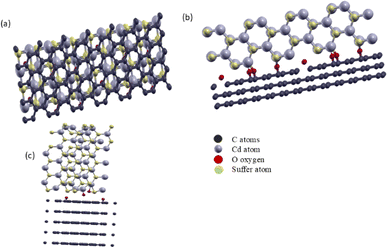 | ||
| Fig. 1 Crystal structure of CdS/GO (a) top view (b) side view for CdS in 110 direction and (c) CdS/GO in 001 direction. | ||
CdS has wurtzite structure, and graphene oxide has hexagonal 2D structure, to avoid the mismatch problem between both structures, we use a 4 × 2 supercell of graphene oxide combined with a 3 × 2 supercell of CdS and CdSe to introduce a minimal mean absolute strain of 2.4% during the optimization of the CdS/GO heterostructure, a notable phenomenon was observed where certain oxygen atoms migrated into the CdS matrix, establishing bonds with Cd atoms. This finding aligns with the experimental results reported by Colina et al.3 Furthermore, it was observed that carbon atoms exhibit a slight displacement within the first plane at the interface with CdS, while the other planes remain unchanged.
To assess the photocatalytic behavior, the valence and conduction band edge were computed using the following empirical equations:22
 | (1) |
| E0VB = E0CB + Eg | (2) |
3 Results and discussion
3.1 CdS, CdSe and GO band structure
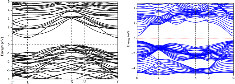
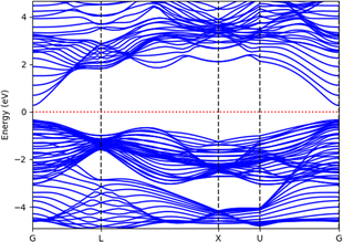
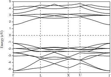
Before analyzing the CdS(Se)/GO heterostructure, the electronic structure of each individual component was examined. Fig. 2 and 3 display the results for CdS and CdSe in the (110) and (001) crystallographic orientations, respectively, with an 8-slab configuration. In the (110) direction, the CdS band gap approximates 0.78 eV with just 2 slabs, gradually increasing with more slabs, where the band gap is indirect. Conversely, CdSe exhibits semiconductor behavior with a direct band gap when using 2 slabs in the same orientation as CdS. In the (001) direction, surface states appear at the Fermi level up to 8 slabs, with the system showing semiconductor characteristics.In Fig. 4, the band structure of CdS along the (110) direction is depicted, by employing the hybrid function (HSE) to rectify the band gap. This adjustment yields a direct band gap of 2.78 eV. The limited number of bands displayed is a consequence of the small number of atoms incorporated into the crystal cell structure. For CdSe the same the behavior was observed, with a band gap of 0.92 eV regarding graphene oxide, it was found that the crucial parameters influencing the band gap and electronic properties are the oxygen contents and the number of graphene layers. Furthermore, the differences are observed between graphene oxide in hexagonal (oxygen at sheet top) and zigzag (oxygen at both sides of carbon sheet) forms, Fig. 5 presents the band structure of GO in hexagonal form with a C/O ratio of 50%.
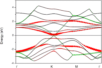 | ||
| Fig. 5 Projected band structure of hexagonal graphene oxide with a C/O ratio of 50%; red and green colors represent the p states of O and C respectively. | ||
The band structure exhibits characteristics such as bandgap opening, which is absent in perfect graphene, and a localized state within the bandgap due to the presence of oxygen groups, affecting the conductivity and optical properties of the material.
3.2 CdS(Se)/GO heterostructure stability
To assess the stability of the CdS/GO or CdS/graphene heterostructure, it is necessary to evaluate several parameters such as lattice mismatch and binding energy. As mentioned, the mismatch and strain were set to 2.4%. To further assess stability, oxygen atoms were introduced at the top of the carbon atoms and the interface binding energy (Eb) was calculated after relaxation as defined in eqn (3):23
 | (3) |
| CdS(001)/GO | CdS(110)/GO | CdSe(110)/GO | CdS/G | CdSe/G | |
|---|---|---|---|---|---|
| Eb (eV per atom) | −30.88 | −0.86 | −3.00 | −0.03 | −0.02 |
3.3 Electronic properties of CdS/GO
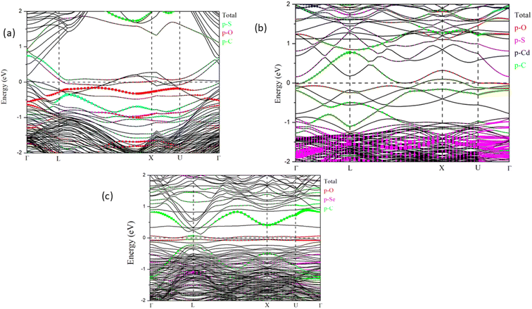
Fig. 6 presents the projected band structure of (a) CdS(001)/GO, (b) CdS(110)/GO and (c) CdSe(110)/GO respectively. As expected, the p states of oxygen atoms are localized near the Fermi level, in conjunction with the p orbitals of carbon atoms while, p states of sulfur are localized between −2 eV and −1 eV, and the d states of cadmium are moved to deep levels.CdS/GO in 001 direction shows metallic behavior, as shown in Fig. 6a, Additionally, the results indicate the formation of surface states near the Fermi level from the p states of C and O, however for 110 direction (Fig. 6b and c) CdS and CdSe keep their semiconductor behavior, and the self-consistent calculations yield band gap values of 0.16 and 0.11 eV, respectively.
CdS along the [001] direction appears to exhibit a surface layer with possible asymmetrical termination, as indicated by the arrangement of Cd and S atoms. This configuration could suggest a polar surface, depending on the stacking sequence and charge distribution within the bulk structure.
In contrast, CdS along the [110] orientation may exhibit a non-polar nature due to balanced terminations. In this case, Cd and S atoms are arranged within the same plane, ensuring that positive and negative charges are evenly distributed and neutralized.
Surface states play a critical role in shaping the electronic properties of thin films, significantly influencing charge carrier transport at the interface between the layer and other materials. Polar surfaces, in particular, often exhibit unique properties, such as strong adsorption, band bending, and surface reconstruction. The charge distribution shows that negative charges are localized on oxygen atoms, creating surface states. These states appear in the band structure as flat bands (Fig. 6b and c), which can enhance electronic mobility and improve electrical conductivity.
3.4 Optical properties. Dielectric function of GO/CdS(Se) heterostructure
The optical properties were computed from dielectric function ε(ω) depicted in eqn (4), which describes the response of a material to an external electric field:24| ε(ω) = ε1 + iε2 | (4) |
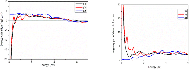
Fig. 7 illustrates the calculation of the real and imaginary parts of the dielectric function for CdS(001)/GO when light is incident from the x, y, and z directions. At high-frequency values, the real part of the dielectric function exhibits a negative value for the polarized electric field along both the x and y axis. Similarly, the imaginary part along the z direction starts at 0.7 eV, indicating significant absorption. Additionally, for both x and y components, there is notable absorption at very low frequencies, which can be attributed to surface states at the CdS–GO interface described above. These observations highlight the intricate interplay of polarization and absorption phenomena at the material and the influence of the CdS/GO interface.
Furthermore, the orientation of the system can control the behavior of the dielectric function, as depicted in Fig. 8, where for CdS(110)/GO, only one component shows a negative value in the real part, while the other components exhibit positive values at lower energies. In addition to anisotropic of the system, this orientation-dependent behavior adds an additional layer of complexity and versatility to the optical properties of the material.
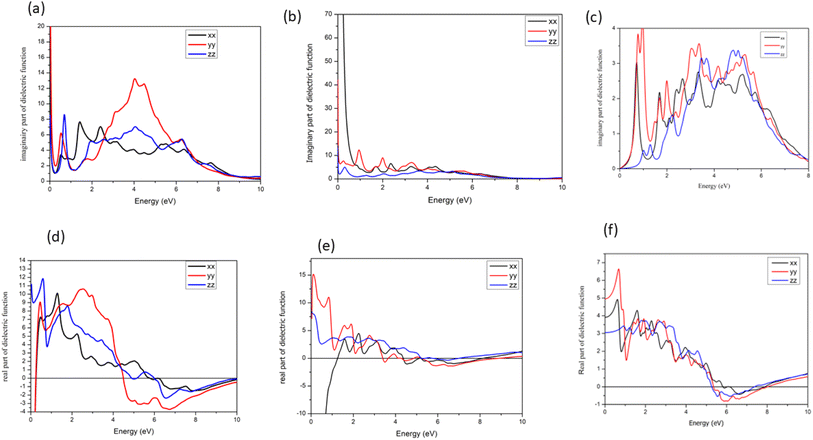 | ||
| Fig. 8 Real (a) and (b) imaginary part of dielectric function of 110 orientations, for CdS and (c) dielectric function of CdSe/GO, (d) imaginary part along x, y and z axis for CdSe/GO. | ||
In contrast of CdSe(110)/GO from the band structure and self-consistent calculation, there is small band gap for CdSe/GO, and this behavior is confirmed in the imaginary part of dielectric function as displayed in (Fig. 8c and d), where the imaginary and real parts of the dielectric function for CdSe/GO are presented for three different directions. Notably, the dielectric constants differ at zero energy along these directions. The absorption characteristics, as illustrated in the imaginary part exhibit similarities for both the x and y directions, a significant difference between CdSe/GO and CdS/GO, particularly in the real part at low energy. The most noteworthy change is the appearance of a negative sign in the real part of CdS/GO, indicating a phenomenon known as “negative permittivity”. This means that the electric field and the induced polarization in the material are in opposite directions, leading to unconventional electromagnetic properties, similarly to the interaction between magnetic field and diamagnetic systems. Such behavior leads to unique optical effects and has a profound influence on the interaction of light with the material.
According to the Debye model, the concept of permittivity connects the displacement vector (D) and the electric field vector (E). The ratio of these amplitudes is described by the permittivity tensor (D/E).
• When ε1 (real part of permittivity) is positive, D and E point in the same direction.
• When ε1 is negative, D and E become perpendicular, leading to unique electromagnetic behaviors.25
In summary, manipulating the CdS orientation offers the potential to mitigate or eliminate the abnormal behavior of the dielectric function observed at low frequencies. This orientation manipulation emerges as a promising strategy for addressing and improving the observed behavior.
3.5 Work function and photocatalytic properties
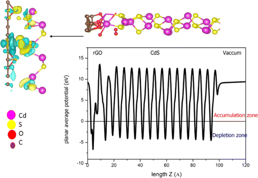
To evaluate the photocatalytic activity for CdSe/GO and CdS/GO heterostructures, we first analyze the overall behavior of the electrostatic potential investigating its average value along z direction as shown in Fig. 9, and the charge density difference which is defined as:| Δρ = ρ(CdS/GO) − ρ(CdS) − ρ(GO) | (5) |
In eqn (5), ρ(CdS/GO) is the electronic charge density for the combined system, ρ(CdS) and ρ(GO) the electronic charge density for CdS and graphene oxide respectively. On the other hand, the work function (Φ) was also computed, expressed as the difference between the energy of the Fermi level (EF) and the energy of the vacuum level (EV).26
| Φ = EV − EF | (6) |
Materials with a high work function are more likely to attract photo-generated electrons to their surface, while materials with a low work function attract holes.27
As shown in Fig. 9, the electronegativity difference between the O and C atoms induces a charge transfer region (indicated by yellow and blue regions) and the development of a dipole moment, oriented from the O atom to the C atom. This establishes a built-in electric field.
To investigate charge transfer across the CdS(001)/GO interface, the work functions of CdS, CdSe and GO are comptued. Due to the higher work function of GO (ϕ = 5.37 eV) compared to CdS (ϕ = 4.73 eV), electrons transfer from CdS to GO, resulting in a dipole moment pointing from GO to CdS, which is antiparallel to the intrinsic dipole moment of GO. In contrast, for CdSe/GO, electron transfer occurs from GO to CdSe.
This charge transfer results in an electron-rich region on the CdS layer's surface, leading to the formation of a two-dimensional electron gas (2DEG).28 The interface shows a significant decrease in potential at 15 Å, accompanied by clear charge redistribution due to the charge depletion on the GO surface. Notably, the most substantial electron depletion occurs at the position of C–O bonds, suggesting that this system may exhibit higher electron mobility.
3.6 Photocatalytic activity
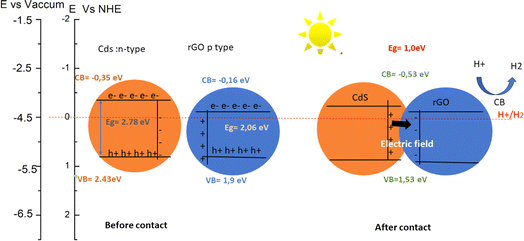
Under illumination, both GO and CdS (CdSe) experience excitation of electrons from their valence bands to their conduction bands. As a result, photo-generated electrons in the conduction band of CdS can spontaneously transfer to the conduction band of GO due to the strong generated electrical force. Simultaneously, photo-generated holes in the valence band of GO transfer to the valence band of CdS(CdSe). This process creates a negatively charged layer on GO and a positively charged layer on CdS, forming an n–p heterojunction. This interfacial charge separation enhances electron–hole photo-generation by suppressing recombination (Fig. 10 and 11). The bands positions for both heterostructures are shifted above the H+/H2 potential, suggesting the potential for hydrogen production.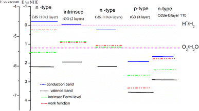 | ||
| Fig. 10 Calculated band edge positions of CdSe, CdS, GO and CdS(Se)/GO with respect to vacuum potential and NHE (Normal Hydrogen Electrode). The green dashed lines are water redox potentials. | ||
The determination of p-type or n-type characteristics in CdS and graphene oxide (GO) relies on factors such as the work function, intrinsic Fermi level, and it's depended on the layer numbers of graphene oxide as well as the O atom ratio. For instance, when a single oxygen atom interacts with CdS, the work function is measured at 5.1 eV. However, upon introducing two oxygen atoms to the CdS matrix, the work function experiences an increase to 5.91 eV. In the case of graphene oxide, with an oxygen ratio of 14%, the band gap and work function stand at 3.17 eV and 4.13 eV, respectively. Upon reducing graphene oxide by 50%, these values undergo a transformation, resulting in a band gap of 0.83 eV and a work function of 3.14 eV. However, the most compelling insights are illustrated in Fig. 10, demonstrating the potential to form either type I or type II heterostructures, dependent to the layer numbers of graphene oxide or CdS orientation. Within the GO layer, surface charge depletion induces observable charge redistribution.
The transferred charge to the Cd–S substrate amplifies the potential on the Cd atoms' side, prompting additional charge transfer from C–O bonds to Cd atoms to maintain equilibrium. Theoretical expectations, depicted in Fig. 11, suggest that the electric field should be oriented from Cd to GO. However, variations in charge density reveal that the electric field orientation depends on the number of oxygen atoms connected to CdS compared to graphene. These findings imply that the controlling the O-to-graphene ratio can enable the manipulation of electric field orientation or charge transfer.
4 Conclusions
Based on the study of the electronic and optical properties and charge transfer dynamic of the CdS/GO and CdSe/GO heterostructures by using DFT calculations while analyzing the obtained results of different physical quantities of interest several conclusions can be drawn:1. Both CdS/GO and CdSe/GO form type II heterostructures, indicating that there is a staggered energy alignment at the interface between the materials. This alignment promotes charge separation and enhances the possibility of hydrogen production.
2. The surface states present in the heterostructures play a crucial role in determining the negative part of the dielectric function at low frequencies. These surface states may influence the overall electronic properties and charge transfer processes.
3. The orientation of CdS combined with graphene oxide can affect the results, potentially altering the electronic structure and charge transport characteristics of the heterostructure. Different configurations may lead to varied energy band alignments and charge separation efficiencies.
Manipulating the oxygen content in the combined system allows control over the band gap of the heterostructure. This can be a valuable approach to fine-tune the electronic properties and optimize the material for specific applications, such as hydrogen production.
Data availability
The data that support the findings of this study are available from the corresponding author, [Hajar Moatassim (E-mail: hajarmoatassim1@gmail.com; ), Felipe Caballero-Briones (fcaballero@ipn.mx)], upon reasonable request.Author contributions
K.·C., H. M., writing – original draft, and curated the data; H. Z., writing – review & editing, formal analysis. M. B. revised the draft and final version A. B.: conceptualization, investigation, review & editing, formal analysis. A. A. E. K.; validation, investigation, formal analysis. M. L. validation, investigation, formal analysis. F. J. E.-F. revised the final version and validated the data. F. C.-B. resources, validation, investigation conceptualized the project, revised the first and final draft, compared the theoretical and experimental data and provided access to LNS supercomputer.Conflicts of interest
There are no conflicts to declare.Acknowledgements
The authors acknowledge Laboratorio Nacional de Supercómputo del Sureste de México (LNS), a member of CONACYT National Laboratories, for the computational resources provided through project no. 202201032n1 and computational resources of HPC-MARWAN (https:\\www.hpc.marwan.ma) provided by the National Center for Scientific and Technical Research (CNRST), Rabat, Morocco. Likewise, M. Boujnah (CVU number 1018873) wants to acknowledge CONACYT-México for his postdoctoral fellowship. FCB acknowledged 2019-40798 grant for financial support.References
- M. Matsuoka, M. Takeuchi, J. Zhang, Y. Horiuchi, M. Anpo and D. W. Bahnemann, Understanding TiO2 Photocatalysis: Mechanisms and Materials, Chem. Rev., 2014, 114(19), 9919–9986, DOI:10.1021/cr5001892.
- L. W. Ching, F. W. M. Keesan and I. I. Muhamad, Optimization of ZnO/GO nanocomposite-loaded polylactic acid active films using response surface methodology, J. King Saud Univ. Sci., 2022, 34(3), 101835, DOI:10.1016/j.jksus.2022.101835.
- R. A. Colina-Ruiz, R. V. Tolentino-Hernández, C. Guarneros-Aguilar, J. Mustre de León, F. J. Espinosa-Faller and F. Caballero-Briones, J. Phys. Chem. C., 2019, 123(22), 13918–13924, DOI:10.1021/acs.jpcc.9b03328.
- N. A. F. Al-Rawashdeh, O. Allabadi and M. T. Aljarrah, Photocatalytic Activity of Graphene Oxide/Zinc Oxide Nanocomposites with Embedded Metal Nanoparticles for the Degradation of Organic Dyes, ACS Omega, 2020, 5(43), 28046–28055, DOI:10.1021/acsomega.0c03608.
- R. A. Moqbel, M. A. Gondal, T. F. Qahtan and M. A. Dastageer, Synthesis of Cadmium Sulfide-Reduced Graphene Oxide Nano-composites by Pulsed Laser Ablation in Liquid for the Enhanced Photocatalytic Reactions in the Visible Light, Int. J. Energy Res., 2018, 42, 1487–1495 CrossRef CAS.
- C. Yamcicier, Z. Merdan and C. Kurkcu, Investigation of the structural and electronic properties of CdS under high pressure: an ab initio study, Can. J. Phys., 2017, 96(2), 216–224, DOI:10.1139/cjp-2017-0257.
- J.-P. Tang, W.-Z. Xiao, L.-L. Wang and X.-F. Li, Half-metallicity in carbon-substituted CdS monolayer, Phys. E, 2014, 59, 230–234, DOI:10.1016/j.physe.2014.01.023.
- L. Jia, D.-H. Wang, Y.-X. Huang, A.-W. Xu and H.-Q. Yu, Highly Durable N-Doped Graphene/CdS Nanocomposites with Enhanced Photocatalytic Hydrogen Evolution from Water under Visible Light Irradiation, J. Phys. Chem. C, 2011, 115(23), 11466–11473, DOI:10.1021/jp2023617.
- L. I. Bendavid, A. O. Atsango and R. W. Smith, Interfacial properties of pure and doped CdS/graphene composites: CdS(0001)/graphene and a CdS/graphene bilayer, Comput. Mater. Sci., 2020, 177, 109537, DOI:10.1016/j.commatsci.2020.109537.
- A. B. Pal, A. K. Rathoure and A. Singh, Investigation of surface interaction in rGO-CdS photocatalyst for hydrogen production: An insight from XPS studies, Int. J. Hydrogen Energy, 2021, 46(53), 26757–26769, DOI:10.1016/j.ijhydene.2021.05.173.
- W. Han, L. Chen, W. Song and S. Wang, Synthesis of nitrogen and sulfur co-doped reduced graphene oxide as efficient metal-free cocatalyst for the photo-activity enhancement of CdS, Appl. Catal., B, 2018, 236, 212–221, DOI:10.1016/j.apcatb.2018.05.021.
- H. An, X. Yan and H. Li, Increased Active Sites by in Situ Growth of CoP Quantum Dots on CdS/rGO To Achieve Efficient Photocatalytic H2 Production, ACS Appl. Energy Mater., 2019, 2(6), 4195–4204, DOI:10.1021/acsaem.9b00439.
- X. Jiang, J. Nisar, B. Pathak, J. Zhao and R. Ahuja, Graphene oxide as a chemically tunable 2-D material for visible-light photocatalyst applications, J. Catal., 2013, 299, 204–209, DOI:10.1016/j.jcat.2012.12.022.
- L. Xu, W.-Q. Huang, L.-L. Wang, Z.-A. Tian, W. Hu, Y. Ma, X. Wang, A. Pan and G.-F. Huang, J. Phys. Chem. C, 2015, 119(51), 28417–28423, DOI:10.1021/acs.jpcc.5b09092.
- P. Giannozzi, et al., QUANTUM ESPRESSO: A Modular and Open-Source Software Project for Quantum Simulations of Materials, J. Condens. Matter Phys., 2009, 21(39), 395502, DOI:10.1088/0953-8984/21/39/395502.
- J. P. Perdew, K. Burke and M. Ernzerhof, Generalized Gradient Approximation Made Simple, Phys. Rev. Lett., 1996, 77(18), 3865–3868, DOI:10.1103/PhysRevLett.77.3865.
- P. E. Blöchl, Projector augmented-wave method, Phys. Rev. B:Condens. Matter Mater. Phys., 1994, 50(24), 17953–17979, DOI:10.1103/PhysRevB.50.17953.
- G. Kresse and D. Joubert, From ultrasoft pseudopotentials to the projector augmented-wave method, Phys. Rev. B:Condens. Matter Mater. Phys., 1999, 59(3), 1758–1775, DOI:10.1103/PhysRevB.59.1758.
- D. R. Hamann, Optimized norm-conserving Vanderbilt pseudopotentials, Phys. Rev. B:Condens. Matter Mater. Phys., 2013, 88, 085117 CrossRef.
- M. Dion, et al., Van der Waals Density Functional for General Geometries, Phys. Rev. Lett., 2004, 92, 246401, DOI:10.1103/PhysRevLett.92.246401.
- D. Stradi, L. Jelver, S. Smidstrup and K. Stokbro, Interface builder in NanoLab: Method for determining optimal supercell representation of interfaces, J. Phys.: Condens. Matter, 2017, 29, 185901, DOI:10.1088/0953-8984/29/18/185901.
- F. Mezzat, H. Zaari, A. El Kenz and A. Benyoussef, Enhanced visible light photocatalytic activity of KTaO3 (Se,V): DFT investigation, Comput. Condens. Matter, 2022, 30, e00648, DOI:10.1016/j.cocom.2022.e00648.
- J.-R. Zhang, Y.-Q. Zhao, L. Chen, S.-F. Yin and M.-Q. Cai, Density functional theory calculation on facet-dependent photocatalytic activity of MoS2/CdS heterostructures, Appl. Surf. Sci., 2019, 469, 27–33, DOI:10.1016/j.apsusc.2018.11.004.
- M. J. van Setten, et al., First-Principles Study of the Optical Properties of MgxTi1–xH2, Phys. Rev. B:Condens. Matter Mater. Phys., 2009, 79(12) DOI:10.1103/PhysRevB.79.125117.
- N. Al-Aqtash, A. Y. Al-Reyahi, S. Al Azar, S. S. Essaoud, M. Maghrabi, A. Mufleh, M. E. Ketfi and K. Berarma, An ab-initio study on the physical properties of double perovskite Cs2AgXBr6 (X = S, Te, Se), Mater. Today Commun., 2024, 38, 108222, DOI:10.1016/j.mtcomm.2024.108222.
- T. Ma, R. Jacobs, J. Booske and D. Morgan, Work Function Trends and New Low-Work-Function Boride and Nitride Materials for Electron Emission Applications, J. Phys. Chem. C, 2021, 125(31), 17400–17410, DOI:10.1021/acs.jpcc.1c04289.
- Q. Xu, L. Zhang, B. Cheng, J. Fan and J. Yu, S-Scheme Heterojunction Photocatalyst, Chem, 2020, 6(7), 1543–1559, DOI:10.1016/j.chempr.2020.06.010.
- J.-R. Zhang, Y.-Q. Zhao, L. Chen, S.-F. Yin and M.-Q. Cai, Density functional theory calculation on facet-dependent photocatalytic activity of MoS2/CdS heterostructures, Appl. Surf. Sci., 2019, 469, 27–33, DOI:10.1016/j.apsusc.2018.11.004.
| This journal is © The Royal Society of Chemistry 2024 |

