
 Open Access Article
 This Open Access Article is licensed under a
 Creative Commons Attribution 3.0 Unported Licence
Gradient aerosol chemical vapor deposition (GA-CVD) for vertically graded thin films of MoxW1−xS2 and WxMo1−xS2†
Abraham
Barde
,
Huda Salam
Al-Jurani
,
Brendan
Ward-O’Brien
 ,
Mark A.
Buckingham
,
Robert
Cernik
and
David J.
Lewis
*
,
Mark A.
Buckingham
,
Robert
Cernik
and
David J.
Lewis
*
Department of Materials, The University of Manchester, Oxford Road, M13 9PL, UK. E-mail: david.lewis-4@manchester.ac.uk
First published on 17th February 2025
Abstract
We report the first gradient aerosol chemical vapor deposition approach to fabricate vertically graded MoxW1−xS2 and WxMo1−xS2 thin films.
Compositionally graded films are a promising class of advanced materials with applications in a range of fields1 such as thermoelectric energy conversion,2 electrocatalysis,3 photoelectrocatalysis,4 photocatalysis,5 photovoltaics,6 photonics,7 optoelectronics,8 sensors,9 corrosion, wear,10 thermal shields,11 and biomedicine.12 Compositionally graded thin films are distinguished from homogeneous thin films by spatial variation in elemental or crystallographic composition. Spatial grading of a thin films composition the may allow optimization of the physical properties of thin films such as electrical and optical properties and thermal transport.4 It may also result in improved efficiencies in, for example, water splitting,3 and enhanced device stability against degradation in challenging environmental conditions.10 Compositional variation can either be lateral (in the x/y-dimension)2,5 or vertical (in the z-dimension),4,6 with the latter far more useful for device fabrication.
In compound semiconductors, particularly isostructural and isoelectronic inorganic semiconductors such as Bi2S3/Sb2S3, MoS2/WS2, or PbS/PbSe, the metal and/or non-metal components can be substituted within the crystal structure with little thermodynamic penalty, allowing control over composition, with negligible impact on phase stability and with crystallographic lattice parameters obeying Vegard's law as a function of mole fraction.8 However, the compositional changes in many cases does have a significant impact on the electronic and/or optical properties of these materials, allowing, for example, bandgap engineering of materials as a function of composition.6,8,13 Compositional control thus enables these semiconductors to be highly tuneable, enabling tailored functional and physical properties, and this has been demonstrated by myriad theoretical, computational, and experimental studies.2,8,13,14
Aerosol assisted chemical vapor deposition (AA-CVD) using single source precursors is a well-developed, effective technique toward thin film deposition.14–16 It has become popular primarily because the requirement for volatile precursors that is crucial in other CVD techniques is relaxed by the nature of the precursor delivery in AA-CVD, and thus a wide range of precursors, often inorganic complexes, have been used to produce materials. Indeed, AA-CVD has been previously exploited to deposit films with laterally graded composition for GaxIn2−xO3,17 and TiO2/SnO25 using in situ precursor mixing and for producing multi-layer films via multiple deposition steps.18 However, to the best of our knowledge, deposition of compositionally graded films in the vertical direction has not yet been achieved using this technique. In this paper, we demonstrate a new aerosol CVD methodology – gradient aerosol chemical vapour deposition (GA-CVD) − which can deposit vertically graded metal sulfide thin films. We use Mo–W–S alloys as an exemplar system to showcase the approach.
The experimental setup for depositing vertically graded thin films is shown in the ESI† (Fig. S3). A programmable precursor feed introduces [Mo(DTC)4] and [W(S)S2(DTC)2] to a digital ultrasonic humidifier. These precursors were chosen as they individually decompose to produce MoS2 and WS2, which are isostructural transition metal dichalcogenides.19–21 They are also able to produce the full range of MoxW1−xS2 alloys when the precursors are co-decomposed in a relatively narrow temperature range commensurate with each other, which has been demonstrated in both solventless thermolysis and in AACVD experiments.13,14,21 The generated aerosol from the dual feed of precursors is carried to the reactor vessel (pre-heated to 450 °C) with an argon carrier gas. This setup allowed the incorporation of both Mo and W into the deposited thin film, with the levels of each element delivered by the precursor feed changing over the course of the experiment. Table S1 (ESI†) gives details of the syringe pump parameters over the course of a typical deposition. By increasing Mo concentration and decreasing W concentration over time in the precursor feed we were able to produce vertically graded MoxW1−xS2 thin films. By increasing W concentration and decreasing Mo concentration over time in the precursor feed, we were able to produce vertically graded WxMo1−xS2 thin films. In both cases, x is defined as 0 at the substrate interface with the metal chalcogenide.
Grazing incidence powder X-ray diffraction (GI-XRD), with an incidence angle of 3° was used to confirm that a single crystalline phase was achieved for both types of graded depositions as shown in Fig. 1(a). Both diffraction patterns were indexed to isostructural hexagonal 2H-molybdenite/tungstenite phases. Reflections centred at ca. 14.3°, 33.3°, 39.0°, 58.6°, and 60.6° were observed, corresponding to the (002), (101), (103), (110), and (112) Bragg planes, respectively.22 We compared this data to that of binary MoS2 and WS2 thin films and a ternary Mo0.5W0.5S2 film which were deposited by standard AA-CVD and characterised by GI-XRD (Fig. S4(a), ESI†). All peaks present in the diffraction pattern can be assigned to the desired material suggesting there were minimal crystalline impurities. Rietveld refinements were also undertaken on all XRD patterns to extract crystalline unit cell parameters. Two isostructural intermetallic phases based on the 2H-molybdenite phase were allowed to refine independently to encompass the broad range of unit cell parameters observed in the sample, until a fit of acceptable quality (Rwp < 10) was reached (Table S2 and Fig. S5, ESI†). The fit predicts that both phases were significantly expanded along the unique axis in comparison to the bulk binary phases (which are very close to one another due to the similar ionic radius of Mo and W), which suggests that there may be significant residual stress within the sample. The final fit also revealed substantial preferred growth in the (002) plane for the one of the included phases and in the (101) plane for the other phase. We observed very similar behaviour when refining the patterns of the binary MoS2 and WS2 (Fig. S4 and S5, ESI†), suggesting the variation is not caused by differences in composition of the film. Preferred orientation in the (002) plane has previosuly been observed in MoWS thin films deposited by AA-CVD.13,19,20 Raman spectroscopy (Fig. 1b) was also used to further confirm molybdenite/tungstenite formation, with peaks associated with the E2g (assigned to WS2, 352 cm−1), E2g (assigned to MoS2, 374 cm−1), and A1g (MoS2/WS2, 415 cm−1) phonons all present, consistent with previously reported Mo–W–S2 alloys.13,14
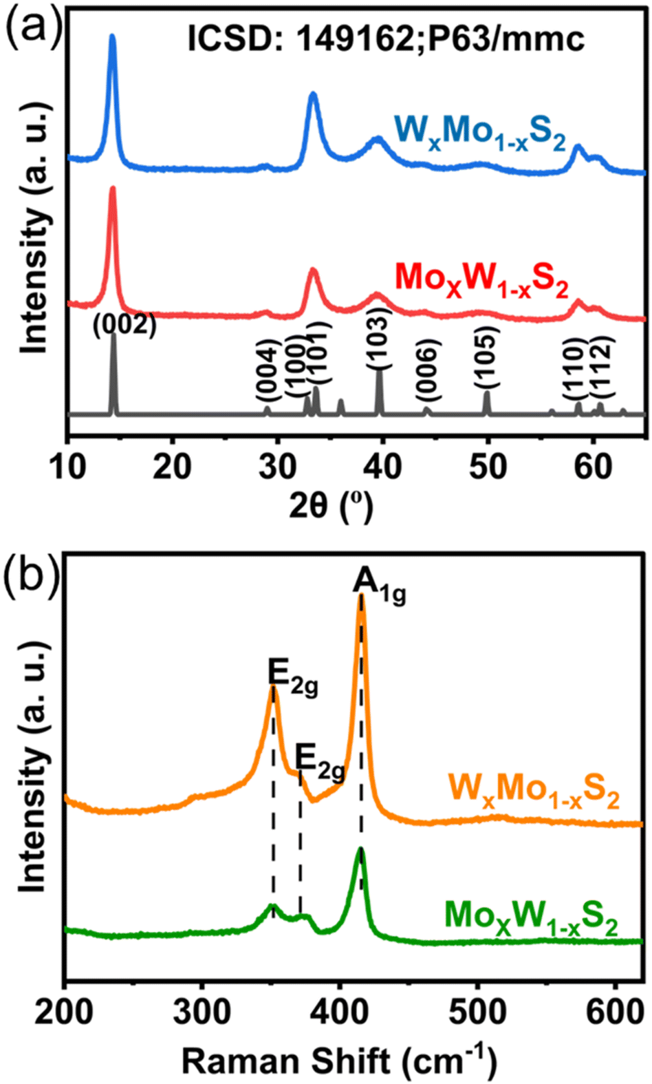 | ||
| Fig. 1 (a) Grazing incidence powder X-ray diffraction (GI-XRD) patterns of MoxW1−xS2 and WxMo1−xS2 thin films compared to a standard 2H-MoS2 powder pattern. (b) Raman Spectra of MoxW1−xS2 and WxMo1−xS2 thin films. | ||
Scanning electron microscopy (SEM) coupled to energy dispersive X-ray (EDX) spectroscopy was used to measure elemental homogeneity laterally across the films. SEM-EDX images are shown in Fig. S9 (ESI†) and show an even incorporation of Mo, W, and S across the thin films.
The morphology of the MoxW1−xS2 and WxMo1−xS2 film surfaces was assessed using secondary electron SEM imaging. The images in Fig. 2(a and b) reveal that densely packed, floret (WxMo1−xS2) and vertically aligned lamellar (MoxW1−xS2) crystallites were formed, which were evenly distributed on the entire substrate. These morphologies are consistent with a previous report of synthesised Mo1–xWxS2 (0 ≤ x ≤ 1) thin films fabricated via AA-CVD.13 Cross-sectional SEM (Fig. S8(a and b), ESI†) imaging showed that a continuous film was deposited, with a thickness of ca. 0.8 μm and 1.5 μm for MoxW1−xS2 and WxMo1−xS2 films, respectively. The discrepancy in the film thickness arises from the fact that WxMo1−xS2 was synthesized using twice the combined molar quantity of precursors compared to that used for MoxW1−xS2 (see Table S1, ESI†). This was intentionally undertaken to demonstrate that compositional gradients can be achieved at varying film thickness, showing the tailorable nature of this method.
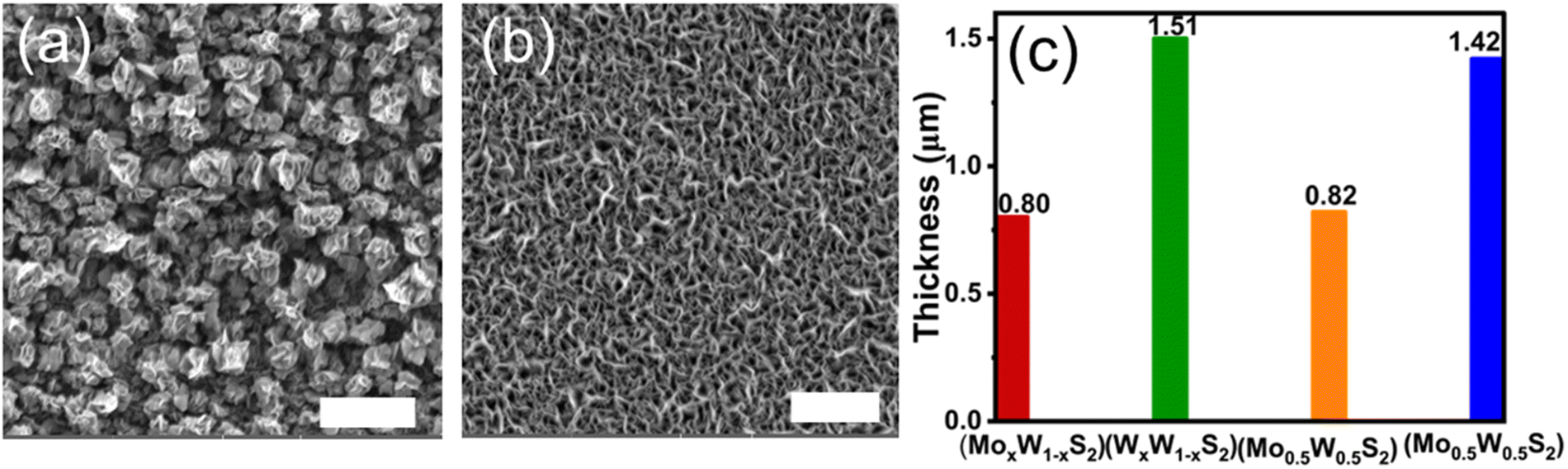 | ||
| Fig. 2 Representative secondary electron (SE) micrographs of the deposited thin films. (a) WxMo1−xS2, (b) MoxW1−xS2, and (c) plots of the thickness of the thin films as measured by cross-sectional SEM, WxMo1−xS2, and MoxW1−xS2. were prepared by GA-CVD and the two Mo0.5W0.5S2 by AA-CVD. The quantity of precursors used for the thin film samples with greater thickness (i.e., the two taller bars) is twice the amount used in preparing the other two thin film with a thickness of ∼0.8 μm. Scale bars represent 5 μm. | ||
Glow discharge optical emission spectroscopy (GDOES) is an ablative elemental analysis technique that was used to investigate the elemental composition of the films as a function of their thickness. The lateral x/y resolution is 500 μm. Fig. 3(a and b) shows that as one metal signal linearly increases in intensity in the z-dimension the other is diminished linearly: this matches with the profile of the delivery of the precursors within the aerosol feed in the production of both MoxW1−xS2 and WxMo1−xS2 films. This depth profile analysis confirms the successful fabrication of crystalline thin films with a vertically graded metal sublattice. As a control experiment, the GDOES elemental depth profiling of Mo and W was also performed on the Mo0.5W0.5S2 thin film deposited with the standard AA-CVD experiment. We found a near constant composition across the whole depth of the film in the z-dimension, with hardly any elemental variation in Mo or W, unlike the compositionally graded films produced by GA-CVD (Fig. S10, ESI†). This, alongside the Raman and GI-XRD data suggest that GA-CVD allows fabrication of vertically graded semiconductor thin films. Given the wide array of extant literature on AA-CVD which includes examples of deposition of inorganic, organic and hybrid materials, it is likely that myriad other functional thin films will now be possible through vertical grading.13,15,16,20
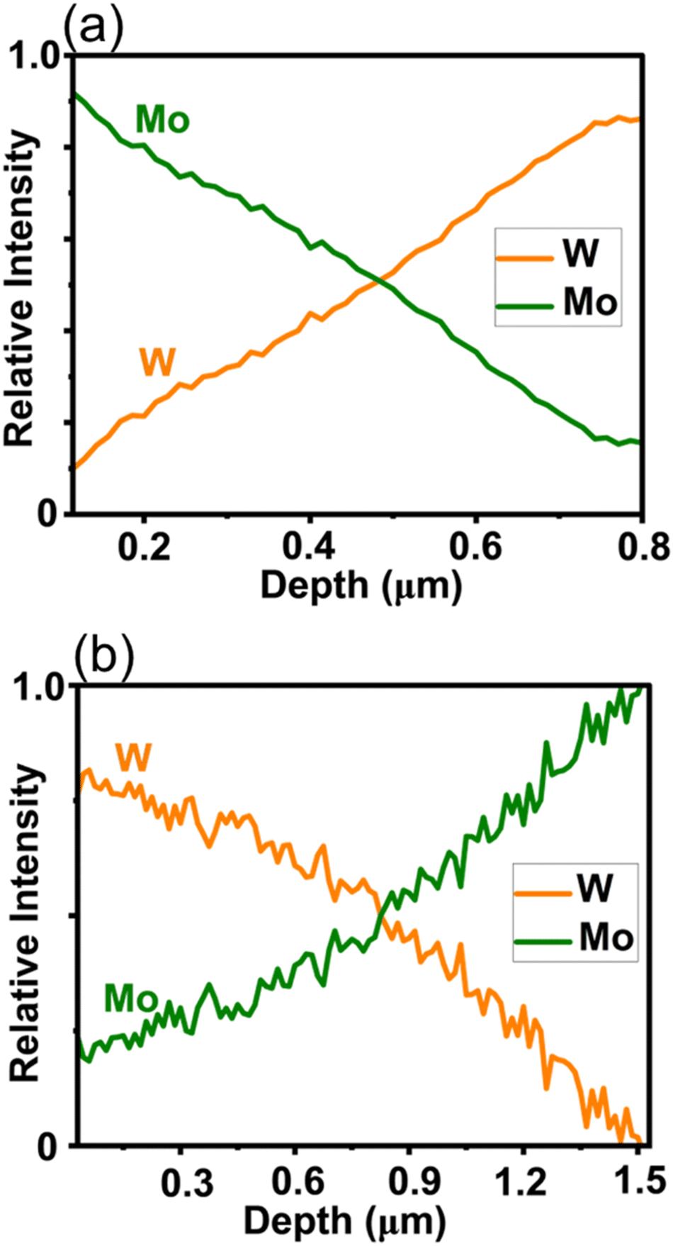 | ||
| Fig. 3 Glow discharge optical emission spectroscopy (GDOES) plots revealing spatial changes in composition of Mo and W as a function of depth in deposited thin films. (a) MoxW1−xS2 and (b) WxMo1−xS2. | ||
In conclusion, a rapid and facile approach – gradient aerosol chemical vapour deposition (GA-CVD) – toward fabricating vertically graded thin films with full compositional control over metal stoichiometry in the z-dimension has been developed. We have demonstrated the utility using the MoxW1−xS2 and WxMo1−xS2 systems (where x = 0 at the substrate-metal chalcogenide interface) as exemplars. Linear control over the metal stoichiometry in the z-dimension has been achieved in these crystalline thin films in both cases. Given the now large library of metal–organic precursors available from the literature on AA-CVD, it is more than likely that GA-CVD can be easily expanded to further materials beyond the MoxWyS2 system. Broadly speaking, this new technique could also overcome the myriad challenges associated with lattice matching strain, adhesion, contamination and stability at the interfaces of successive depositions that have been observed perennially in the CVD literature, the elimination of which are important in the manufacture of semiconductor devices.23
Conceptualisation: D. J. L.; methodology: A. B., D. J. L.; experimental design: A. B.; data collection and analysis: A. B., H. S. A.-J., B. W. O’B., M. A. B., R. C., D. J. L.; funding acquisition: A. B.; supervision: D. J. L.; validation: A. B., B. W. O’B., M. A. B., D. J. L; visualisation: A. B., B. W. O’B; writing original draft: A. B.; D. J. L.; review and editing: all authors.
A. B. would like to thank the PTDF Overseas Scholarship Scheme for a PhD scholarship award (PTDF/ED/OSS/PHD/AB/1782/2020PHD090). B. W-O'B. would like to thank the EPSRC for a DTP studentship.
Data availability
Data can be made available upon reasonable request.Conflicts of interest
There are no conflicts to declare.Notes and references
- B. Saleh, J. Jiang, R. Fathi, T. Al-hababi, Q. Xu, L. Wang, D. Song and A. Ma, Composites, Part B, 2020, 201, 108376 CrossRef.
- C. Ou, L. Zhang, Q. Jing, V. Narayan and S. Kar-Narayan, Adv. Electron. Mater., 2020, 6, 1900720 CrossRef CAS.
- S. M. Tan and M. Pumera, ACS Appl. Mater. Interfaces, 2017, 9, 41955–41964 CrossRef CAS PubMed.
- Y. Xiao, Z. Fan, M. Nakabayashi, Q. Li, L. Zhou, Q. Wang, C. Li, N. Shibata, K. Domen and Y. Li, Nat. Commun., 2022, 13, 7769 CrossRef CAS PubMed.
- N. Chadwick, S. Sathasivam, A. Kafizas, S. M. Bawaked, A. Y. Obaid, S. Al-Thabaiti, S. N. Basahel, I. P. Parkin and C. J. Carmalt, J. Mater. Chem. A, 2014, 2, 5108–5116 RSC.
- S.-C. Yang, M. Ochoa, R. Hertwig, A. Aribia, A. N. Tiwari and R. Carron, Prog. Photovolt.: Res. Appl., 2021, 29, 630–637 CrossRef CAS.
- B. K. Singh, V. Bambole, V. Rastogi and P. C. Pandey, Opt. Laser Technol., 2020, 129, 106293 CrossRef CAS.
- K. Bogaert, S. Liu, T. Liu, N. Guo, C. Zhang, S. Gradečak and S. Garaj, Sci. Rep., 2018, 8, 12889 CrossRef PubMed.
- E. Müller, Č. Drašar, J. Schilz and W. A. Kaysser, Mater. Sci. Eng., 2003, 362, 17–39 CrossRef.
- A. Hadipour, M. Rahsepar and H. Hayatdavoudi, Surf. Eng., 2019, 35, 883–890 CrossRef CAS.
- M. Sathish, N. Radhika and B. Saleh, Composites, Part B, 2021, 225, 109278 CrossRef CAS.
- H. Shi, P. Zhou, J. Li, C. Liu and L. Wang, Front. Bioeng. Biotechnol., 2020, 8, 616845 CrossRef PubMed.
- A. A. Tedstone, E. A. Lewis, N. Savjani, X. L. Zhong, S. J. Haigh, P. O’Brien and D. J. Lewis, Chem. Mater., 2017, 29, 3858–3862 CrossRef CAS.
- N. Zeng, Y.-C. Wang, J. Neilson, S. M. Fairclough, Y. Zou, A. G. Thomas, R. J. Cernik, S. J. Haigh and D. J. Lewis, Chem. Mater., 2020, 32, 7895–7907 CrossRef CAS PubMed.
- W. Xiao, M. A. Buckingham, Y. Li, K. Hazeldine, B. Han, S. H. Cartmell, A. S. Eggeman, A. S. Walton and D. J. Lewis, Chem. Commun., 2023, 59, 12427–12430 RSC.
- A. Barde and D. J. Lewis, J. Phys. Chem. C, 2023, 127, 13969–13977 CrossRef CAS.
- C. E. Knapp, A. Kafizas, I. P. Parkin and C. J. Carmalt, J. Mater. Chem., 2011, 21, 12644–12649 RSC.
- J.-G. Song, G. H. Ryu, S. J. Lee, S. Sim, C. W. Lee, T. Choi, H. Jung, Y. Kim, Z. Lee, J.-M. Myoung, C. Dussarrat, C. Lansalot-Matras, J. Park, H. Choi and H. Kim, Nat. Commun., 2015, 6, 7817 CrossRef PubMed.
- D. J. Lewis, A. A. Tedstone, X. L. Zhong, E. A. Lewis, A. Rooney, N. Savjani, J. R. Brent, S. J. Haigh, M. G. Burke, C. A. Muryn, J. M. Raftery, C. Warrens, K. West, S. Gaemers and P. O’Brien, Chem. Mater., 2015, 27, 1367–1374 CrossRef CAS.
- G. Murtaza, S. P. Venkateswaran, A. G. Thomas, P. O'Brien and D. J. Lewis, J. Mater. Chem. C, 2018, 6, 9537–9544 RSC.
- N. E. Richey, C. Haines, J. L. Tami and L. McElwee-White, Chem. Commun., 2017, 53, 7728–7731 RSC.
- K. G. Mondal, B. S. Kar, S. Rakshit, S. Saha, P. C. Jana and M. N. Goswami, J. Alloys Compd., 2023, 969, 172356 CrossRef CAS.
- G.-H. Park, K. Nielsch and A. Thomas, Adv. Mater. Interfaces, 2018, 6, 1800688 CrossRef.
Footnote |
| † Electronic supplementary information (ESI) available. See DOI: https://doi.org/10.1039/d5cc00237k |
| This journal is © The Royal Society of Chemistry 2025 |