DOI:
10.1039/D5CE00466G
(Paper)
CrystEngComm, 2025,
27, 4649-4667
Acoustic shock wave-induced dynamic recrystallization facilitating reconstructable phase transition from zinc blende to rocksalt in cadmium telluride
Received
5th May 2025
, Accepted 7th June 2025
First published on 18th June 2025
Abstract
Cadmium telluride (CdTe) is a promising material for solar cells; however, its stability is compromised under high pressure and temperature, leading to structural and electronic damage, including degradation. The current study aims to investigate the behavior of CdTe under acoustic shock waves with 0.59 MPa pressure, 529 K temperature, and 1.5 Mach number by focusing on its structural, optical, and morphological properties. Techniques such as X-ray diffraction (XRD), Raman spectroscopy, UV-vis diffuse reflectance spectroscopy (DRS), photoluminescence (PL) spectroscopy, and field emission scanning electron microscopy (FE-SEM) were employed to analyze the material's response. The overall XRD and Raman results reveal that CdTe undergoes a reconstructable phase transition from cubic-zincblende (ZB) to cubic-rocksalt (RS) under shock wave exposure. Optical analysis revealed a reduction in the bandgap, and a shift in PL emission was observed. Morphological changes observed due to shock waves induced by dynamic recrystallization were noted after 300 shock pulses, followed by the restoration of the layered structure at 400 shock pulses. These findings highlight the reconstructable nature of phase transitions and emphasize the importance of addressing degradation pathways to improve CdTe's long-term stability and efficiency in solar cells. The observed reconstructable phase transition offers a potential method for tuning CdTe's properties under acoustic shock wave exposure.
Introduction
Over half a century ago, cadmium telluride (CdTe) significantly emerged as a most promising material for solar cell applications, largely due to its remarkable optical absorption properties.1 CdTe, classified as an II–VI semiconducting compound belonging to the chalcogenide group of the family, exhibits exceptionally high optical absorption coefficients. This characteristic enables it to efficiently capture a significant portion of the solar spectrum, even when only a thin material layer is used.2 The ability to achieve such high absorption efficiency with minimal material usage will significantly reduce both material requirements and production costs. As a result, CdTe has become a strong competitor compared to other traditional silicon-based solar cells in terms of cost-effectiveness and performance. Although CdTe poses ecological concerns due to its toxicity, it remains a robust and chemically stable semiconductor, and the material's compatibility with scalable and industrial manufacturing techniques has established it as a leading candidate for developing cost-effective solar energy solutions on a large scale.3,4 Since CdTe is best known for its role in photovoltaics, its utility extends well beyond this domain. It has been extensively applied in technological areas like sensors and detectors, demonstrating its versatility in addressing various technological needs.5,6 The material has gained further attention in recent eras due to its potential applications in advanced technological fields. Researchers have explored its suitability as a functional component in optoelectronic systems, where its unique properties enable the design of efficient light-absorbing and energy-converting devices. The application of CdTe in photovoltaic nanodevices has also become a rapidly expanding area of research, reflecting its adaptability and potential in upcoming energy systems for next-generation.7,8 Within the realm of solar cells, CdTe plays a critical role in enhancing energy conversion efficiency, further solidifying its position as a pivotal material in the ongoing development of solar technology.9–11 It is most valued for its role in specialized applications such as electro-optics, photorefractive devices, room-temperature radiation detectors,12 solar panels,13 and gamma/X-ray detectors,14,15 highlighting its broad utility and technological significance.
Despite its potential, sometimes it can degrade under ambient atmosphere due to moisture and oxygen exposure, leading to forms of CdO and TeO2. This degradation is slower at room temperature, which impacts the optical property.16 At high pressure and temperature exposure, the degradation process accelerates with increased oxidation rates. The elevated temperature promotes faster formation of CdO and TeO2, leading to greater structural and electronic damage. This results in a decline in CdTe's performance, particularly in solar cell applications.17 Other major drawbacks in synthesizing high-quality, stoichiometric CdTe remain challenging due to issues like imbalances in the Cd![[thin space (1/6-em)]](https://www.rsc.org/images/entities/char_2009.gif) :Te ratio, which can lead to intrinsic defects such as vacancies that impair carrier mobility and increase leakage currents. Achieving large, chemically homogeneous crystals with precise stoichiometry and uniformity across various synthesis methods adds to the complexity.18 Also, CdTe-based detector has serious issues such as micro-crystallinity, where small grains create grain boundaries that disrupt charge transport and hinder detectors' performance. High defect densities introduce recombination centers that reduce carrier lifetimes and sensitivity. More impurities will be introduced during the synthesis process at localized energy levels, degrading the material's electronic properties. Collectively, these factors degrade the structural and electronic properties of CdTe, limiting its effectiveness in high-performance applications. These difficulties have slowed the advancement of CdTe-based devices, particularly those requiring large-area or high-performance materials. However, significant improvements in conventional and unconventional methods over the past decades have allowed for better control over the material's properties, increasing its potential for broader use and enhanced performance.19
:Te ratio, which can lead to intrinsic defects such as vacancies that impair carrier mobility and increase leakage currents. Achieving large, chemically homogeneous crystals with precise stoichiometry and uniformity across various synthesis methods adds to the complexity.18 Also, CdTe-based detector has serious issues such as micro-crystallinity, where small grains create grain boundaries that disrupt charge transport and hinder detectors' performance. High defect densities introduce recombination centers that reduce carrier lifetimes and sensitivity. More impurities will be introduced during the synthesis process at localized energy levels, degrading the material's electronic properties. Collectively, these factors degrade the structural and electronic properties of CdTe, limiting its effectiveness in high-performance applications. These difficulties have slowed the advancement of CdTe-based devices, particularly those requiring large-area or high-performance materials. However, significant improvements in conventional and unconventional methods over the past decades have allowed for better control over the material's properties, increasing its potential for broader use and enhanced performance.19
Numerous traditional and unconventional methods are used to enhance the material's properties. The traditional methods are the hot wall deposition technique,20 spray pyrolysis,21 cathodic electrodeposition,22 thermal evaporation technique,23 chemical bath deposition,24 and high pressure/unconventional methods such as static high pressure,25 laser shock waves,26 gamma irradiation,27 acoustic shock waves,28,29etc. For instance, CdTe and Zn-doped CdTe nanoparticles were synthesized by the chemical reduction method. Comparing the two, Zn-doped CdTe exhibited improved photosensitivity and reduced recombination compared to undoped CdTe. Hibiscus mutabilis extract, used as a natural dye, enhanced light absorption in dye-sensitized solar cells (DSSCs). Zn doping further increases the efficiency of the DSSCs, with better performance observed in the doped samples.30 Dharmadasa et al. reported that CdTe was effectively synthesized by electrodeposition (ED) with a two-electrode system to avoid reference electrode impurities. This method enables the growth of rod-type or columnar grains that are beneficial for electronic devices. Also, PEC cell studies showed that CdTe can be deposited in n-type, i-type, and p-type forms by adjusting the growth voltage. CdCl2 heat treatment induced a transition from n-type to p-type CdTe, enhancing conductivity. Structural changes at 385 °C led to larger grains and an efficiency peak of 12%. Further treatment improved crystallinity, achieving efficiencies of over 15%. Photoluminescence studies confirmed defect reduction, aligning with efficiency improvements. Over results show that rod-shaped materials and graded bandgap structures improve charge carrier generation, leading to higher solar cell efficiencies in the future.31 CdTe bulk material was grown using vapor deposition synthesis (VDS), yielding a stoichiometric, single-phase cubic structure with a smooth, void-free surface. Thin films, fabricated by thermal evaporation, were uniform, polycrystalline with fine grains, and showed semiconducting behavior in I–V studies, highlighting their potential for biosensor applications.32 Sn-doped CdTe thin films were successfully produced using a low-cost, homemade, close-spaced sublimation (CSS) system. This process introduced sub-bandgap states and tuned structural and morphological properties without altering the CdTe phase, enhancing optical absorption for optoelectronic and solar cell applications.33 Unconventional high-pressure methods have also been explored. CdTe was examined under high pressure using DFT, focusing on structural, electronic, elastic, and phonon properties. CdTe transitions from a semiconducting wurtzite structure (P63mc) to a stable metallic cubic phase (Fm-3m) at 10 GPa and an unstable orthorhombic phase (Cmmm) at 140 GPa. Phase transformation paths were predicted for the first time. Above all other phases, the cubic phase enhances electrical conductivity, thereby improving electron mobility.34 CdTe structural property was studied using synchrotron radiation, revealing structural transitions were observed near 3.5 GPa from zinc-blende to cinnabar, then from cinnabar to NaCl. The cinnabar phase features site ordering of Cd and Te atoms with near fourfold coordination. This structural change enhances the material's adaptability under pressure. The discovery of this phase suggests the potential for improved high-pressure applications.35
In contrast to traditional methods, acoustic shock waves have emerged as a prominent technique in solid-state material research in the 21st century. Traditional synthesis methods often take a long time, which can induce impurities and extend processing durations. On the other hand, in unconventional methods, laser shock wave compression operates on a nanosecond time scale, offering a compression rate several orders of magnitude higher than the static method's rate. In comparison, acoustic shock waves offer a compression time scale ranging from milliseconds to microseconds. This shows that there has been a relentless search for materials studied under acoustic shock waves, and shock wave experiments have become a beacon of hope for many researchers.36–38
There is a lack of research on the behavior of acoustic shock waves on CdTe, highlighting a major research gap in the current literature. In this work, we aim to bridge this gap by conducting a detailed investigation into the structural, optical, and morphological behavior of CdTe by exposing acoustic shock waves. This research explores the material's response to extreme conditions, providing insights into its potential applications. CdTe was subjected to a series of shock pulses (100, 200, 300, and 400), with a pressure of 0.59 MPa, a temperature of 520 K, and a Mach number of 1.5, to evaluate how varying shock pulses affect the material's properties.
Experimental section
Cadmium telluride (CdTe) was purchased commercially from SRL with 99.9% purity and used as it is without further purifications for investigation under acoustic shock wave conditions. The acoustic shock waves were generated using a tabletop semi-automatic Reddy tube, comprising three key sections: the driven section, the diaphragm section, and the driver section. An 80 GSM paper diaphragm served as the rupture medium for this experiment. The CdTe sample was placed 1 cm away from the drive section's open end in a sample holder. When the pressure in the driver section reached the critical threshold, the diaphragm ruptured, producing shock waves. The CdTe sample was subjected to four shock pulse sets, comprising 100, 200, 300, and 400 shock pulses. A transient pressure and temperature per shock pulse were recorded using piezoelectric PCB transducers (Model 113B26) with a sensitivity of 1.465 mV kPa−1 and a linearity error of 1%. To ensure measurement accuracy, the transducers were calibrated under high transient pressure and transient temperature. This calibration involved comparing the transducer response with a standard reference, maintaining a standard error below 5% for consistency. These measures ensured high reliability and repeatability in transient pressure measurements, providing a precise reference for analyzing the effects of shock pulses on the samples. The schematic representation of the semiautomatic Reddy tube is shown in Fig. 1. To analyze the effects of shock waves, CdTe samples were characterized pre- and post-shock wave exposure using techniques such as powder X-ray diffraction (XRD), Raman spectroscopy, UV-vis diffuse reflectance spectroscopy (DRS), photoluminescence (PL) spectroscopy, and field-emission scanning electron microscopy (FE-SEM).
 |
| | Fig. 1 The schematic representation of the semiautomatic Reddy tube. | |
Characterization technique details
Powder X-ray diffraction (XRD) pattern of CdTe pre- and post-shock wave exposure is recorded using a Bruker D2 Phaser X-ray powder diffractometer model with a CuKα1 source and 1.54 Å wavelength, in the range of 20° to 80° and with a step size of 0.02°. XRD techniques were used to analyze the structure of CdTe pre- and post-shock wave exposure and observe possible phase changes under shock wave exposure. The XRD pattern of CdTe pre- and post-shock wave exposure was refined using FullProf software. The refinement incorporated two structural models: the cubic-zincblende structure with the F-43m space group (Crystallography Open Database ID 1010539) and the cubic-rocksalt structure with the Fm-3m space group (COD ID 1010536).
Raman spectra of CdTe pre- and post-shock wave exposure were acquired using a 532 nm (50 mW) laser source with Renishaw confocal Raman microscopy. The system's axial resolution was <1 μm, and the lateral resolution was 0.5 nm. Spectral data were recorded in the range of 100–1000 cm−1. The Raman measurements were conducted to analyze the structural changes, and this setup allowed detailed observation of the material's vibrational modes of CdTe pre- and post-shock wave exposure.
UV-vis diffuse reflectance spectroscopy (DRS) analysis of CdTe pre- and post-shock wave exposure was conducted using a SHIMADZU UV-5600 PLUS UV-vis NIR spectrophotometer. The instrument measures across a wide wavelength range of 185–3300 nm. For this study, spectral data were recorded within the 300–800 cm−1 range to assess changes in the optical properties of CdTe pre- and post-shock wave exposure.
Photoluminescence (PL) spectra of CdTe pre- and post-shock wave exposure were recorded using a PERKIN ELMER PL 6500 with a wavelength range of 190–900 nm, accuracy of 0.5 nm, reproducibility of 0.2 nm, and a resolution of 1 nm. Measurements were conducted in real time with a high scan speed of up to 24000 nm min−1. The spectra, recorded between 400 and 800 nm, were analyzed to investigate atomic defects. These results provided insights into how defects influence the material's optical properties of CdTe pre- and post-shock wave exposure.
Field emission scanning electron microscopy (FESEM) of CdTe pre- and post-shock wave exposure was performed using a SIGMA HV – Carl Zeiss system equipped with a Bruker Quantax 200 – Z10 EDS detector. The instrument operated at an accelerating voltage range of 200 V to 30 kV, with magnifications from 20× to 1000000×. It provided a resolution of 1.0 nm at 30 kV and 3 nm at 1 kV and a maximum probe current exceeding 100 nA. The 2D surface profile of CdTe pre- and post-shock wave exposure was generated using mountainsLab software. FESEM analysis aimed to examine CdTe's morphology and elemental composition pre- and post-shock wave exposure, and to observe the morphology changes due to shock wave exposure.
Results and discussion
Structural analysis: X-ray diffraction (XRD)
Fig. 2 provides the XRD pattern of CdTe pre-shock wave exposure with a standard pattern and the cubic-zincblende (ZB) structure of CdTe. The obtained XRD pattern is compared with the standard JCPDS card number 75-2086; the XRD pattern aligned well with the standard pattern. It confirms that CdTe has a zincblende (ZB) crystal structure, specifically a sphalerite structure, and crystallizes in the face-centered cubic (FCC) with an F-43m space group. The space group F-43m says that ‘F’ represents a face-centered cubic (FCC) lattice with tetrahedral symmetry, featuring four threefold rotational axes aligned along three mirror planes intersecting the body diagonals of the cube it is represented by 43m.39 The lattice parameters are a = b = c = 6.410 Å and the volume is 263.37 Å3.
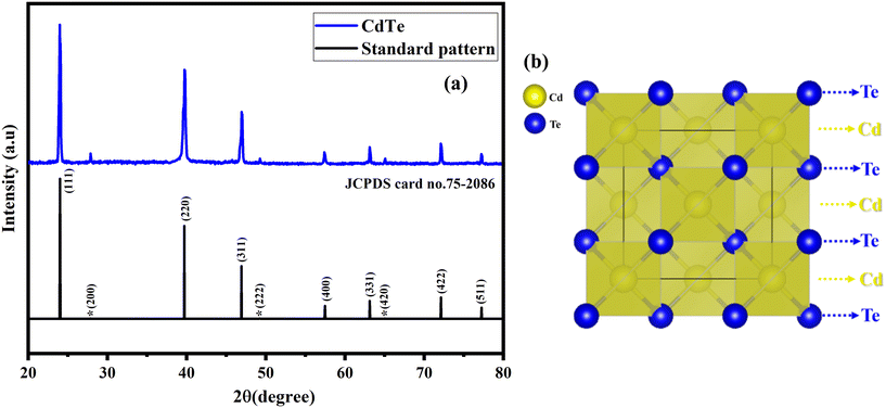 |
| | Fig. 2 XRD pattern and structure of CdTe (a) pre-shock wave exposure with a standard pattern, and (b) cubic-zincblende (ZB) structure of CdTe. | |
In this configuration, CdTe is covalently bonded in a repeating sequence of Te–Cd–Te–Cd, held together by van der Waals forces.40 Each Cd2+ ion is tetrahedrally coordinated to four equivalent Te2− ions, forming CdTe4 tetrahedra that share corners. Similarly, each Te2− ion is tetrahedrally coordinated to four equivalent Cd2+ ions, forming TeCd4 tetrahedra, and the structure is less symmetric. The Te2− anion forms covalent bonds with the Cd2+ cations, where each Cd2+ ion is equivalently bonded to four Te2− ions, and each Te2− ion is equivalently bonded to four Cd2+ ions.41 The shock loading tests examine how well it holds its structure and properties under acoustic shock waves. This helps us understand its response to extreme conditions. Fig. 3 illustrates the XRD pattern of CdTe pre- and post-shock wave exposure with cubic-zincblende (ZB) and cubic-rocksalt (RS) structure. A notable change in diffraction peak intensity was observed after shock wave exposure, particularly in the (111), (200), (311), (222), (331), (420), and (511) planes. Fig. 4 shows the zoomed version of (111), (200), (311), (222), (331), (420), and (511) planes. A significant reduction in diffraction intensity occurred in the (111), (311), (331), and (511) planes. Conversely, a markable increase in intensity was noted in the (200), (222), and (420) planes. The diffraction peak intensity varies due to shock wave-induced rapid compression, which triggers dynamic recrystallization and results in the reorganization of atoms within the crystal lattice,42Fig. 5 shows the zoomed version of (111), (200), (311), (222), (331), (420), (511) planes of CdTe (zincblende) and 300 shock pulses (rocksalt) with standard pattern. These variations became more pronounced after exposure to 300 shock pulses. These changes indicate that the acoustic shock waves affect the crystallographic plane, leading to variations in their structural properties. Generally, peak intensity in XRD suggests the arrangement of atoms in the crystal lattice.43 A change in peak intensity may signify a structural change, such as an atomic rearrangement, without any appearance or disappearance of new diffraction peaks. So, it confirms that at 300 shock pulses, phase transitions were observed, and the zincblende structure was transformed into a rocksalt structure. The primary difference between the two structures is the arrangement of atoms in the crystal lattice, although both are cubic. The space group differs between the two structures. The obtained diffraction peaks and their intensity are well-matched with the JCPDS card number 75-2083. The lattice parameters are a = b = c = 6.410 Å, and the volume is 263.37 Å3. At 300 shock pulses, CdTe adopts a rock salt (RS) crystal structure, crystallizing in a face-centered cubic (FCC) arrangement with an Fm-3m space group, commonly recognized as the rocksalt structure (RS).44,45 The Fm-3m space group represents a face-centered cubic (FCC) lattice with high symmetry. It includes mirror planes, threefold rotational axes, and inversion centers, ensuring uniformity in all directions. It contributes to isotropic properties and structural stability. In this configuration, CdTe forms a symmetrical rocksalt pattern arranged octahedrally. Six Te2− ions surround each Cd2+ ion in an octahedral geometry, and similarly, each Te2− ion is surrounded by six Cd2+ ions, creating an alternating Cd–Te–Cd–Te arrangement. This pattern forms a face-centered cubic (FCC) framework.46,47
 |
| | Fig. 3 XRD pattern of CdTe (a) XRD pattern of CdTe pre- and post-shock wave exposure with standard patterns (b) cubic-zincblende (ZB) and cubic-rocksalt (RS) structure. | |
 |
| | Fig. 4 Zoomed version of (111), (200), (311), (222), (331), (420), and (511) planes. | |
 |
| | Fig. 5 Zoomed version of (111), (200), (311), (222), (331), (420) planes of control CdTe (zincblende) and 300 shock pulses (rocksalt) with standard patterns. | |
Fig. 6 shows the mechanism of reconstructable phase transition induced by the acoustic shock wave from cubic-zincblende (ZB) to cubic-rocksalt (RS). Fig. 6(a) shows the cubic zincblende structure, where each Cd atom is tetrahedrally bonded to four Te atoms. Shock wave-induced rapid lattice compression causes thermal energy, which leads to weak van der Waals forces between Cd and Te bonds breaking, resulting in lattice distortion. This distortion causes Cd atoms to shift from their original tetrahedral positions to octahedral sites. In this new octahedral arrangement, each Te atom is surrounded by six nearest Cd atoms, leading to a structural transformation into the more uniform rocksalt phase with octahedral coordination. Additionally, a reduction in lattice parameters is observed. Despite the change, the overall cubic crystallization remains intact, as seen in Fig. 6(b) and (c). With 400 shock pulses, the Cd atoms were restored from the octahedral to their original tetrahedral positions. This restoration leads to a reconstructable/reversible structural transition, which eventually reverts to the zincblende structure, which is shown in Fig. 6(d). Acoustic shock wave-induced lattice compression can cause lattice distortion and break weak bonds, allowing the material to return to its original structure due to lattice relaxation/expansion.48,49 The material undergoes a phase transition due to rapid energy transfer induced by acoustic shock waves, all occurring within milliseconds. When a shock pulse is applied to the sample, it generates thermal energy. As a result, the molecules absorb thermal energy, leading to an increase in their vibrational energy, which, in turn, causes some level of disorder in the crystal lattice. This initial vibrational disorder lays the groundwork for more significant structural responses, especially in materials with low thermal conductivity and diffusivity.50 CdTe exhibits low thermal conductivity (6.2 W m−1 K−1) and low thermal diffusivity (1.4 × 10⁻⁷ m2 s−1), and heat dissipation is limited. This limitation causes thermal energy to cause localized heat that facilitates dynamic recrystallization, defect reorganization, and structural modification as shock waves continue to propagate through the crystal lattice, and the material attains a molten state. At 100 shock pulses, the energy is insufficient to disturb the atomic lattice significantly or excite the molecules to higher energy states. As a result, the material remains in a lower energy state, and only minor lattice strain and isolated point defects form at the microstructural level. There is no notable phase transitions observed at this stage. At 200 shock pulses, the energy is sufficient to initiate early-stage atomic-level instabilities. These changes mark the beginning of structural evolution but remain below the threshold for dynamic recrystallization or electron excitation. At 300 shock pulses, the energy reaches a critical threshold. The rapid deposition of energy, combined with CdTe's low thermal conductivity and diffusivity, prevents efficient heat dissipation. As a result, superheating occurs, where the material's temperature exceeds its equilibrium melting point without complete melting, leading to a premelting state characterized by significant atomic disorder. At this stage, the energy input is sufficient to excite atoms and molecules to higher energy states, destabilizing the original zincblende crystal structure. As atomic order continues to break down, the material briefly enters a transient molten state. Upon rapid cooling, the atoms cannot return to their original positions and instead undergo dynamic recrystallization, reorganizing into a new, more stable configuration.50 This process drives the phase transition to the rocksalt structure, which remains stable under ambient conditions. Thus, the combined effects of superheating, atomic excitation, partial melting, and recrystallization govern the complete structural transformation observed. At 400 shock pulses, energy redistribution occurs, leading to a reversible phase transition. Due to the material's low thermal conductivity and diffusivity, heat dissipation remains gradual. This facilitates complete defect reorganization and atomic rearrangement, allowing the excited molecules to relax to lower energy states. As a result, the crystal lattice regains its original order, reverting to its initial phase. This sequence of events explains the phase transition observed at 300 shock pulses and also the reversion to the original phase at 400 shock pulses.
 |
| | Fig. 6 Mechanism of reconstructable phase transition induced by acoustic shock wave from cubic-zincblende (ZB) to cubic-rocksalt (RS). | |
Fig. 7 shows Rietveld's refinement of CdTe pre- and post-shock wave exposure. The XRD pattern of CdTe, pre- and post-shock wave exposure, was refined using FullProf software. Pre-shock, CdTe exhibits a cubic-zincblende structure (F-43m space group), stable up to 200 shock waves. At 300 shock pulses, the structure transforms into a cubic-rocksalt structure (Fm-3m), which then reverts to the original cubic-zincblende structure (F-43m), confirming structural and reconstructable phase transitions. The calculated lattice parameter and unit cell volume are shown in Table 1. Under acoustic shock wave exposure, lattice parameters and unit cell volume fluctuations were observed. At 100 and 200 shock pulses, the lattice parameters (a, b, c) and volume (V) slightly decreased. However, at 300 shock pulses, there was a considerable decrease due to lattice contraction.51 This reduction indicates that the material underwent lattice contraction, causing lattice distortion and a phase transition. At 400 shock pulses, the lattice parameters increased due to shock wave-induced expansion,52 restoring the distorted lattice and confirming the reconstructable phase transition. The lattice parameter and unit cell volume are directly proportional to each other; the variation plot against the number of shock pulses is shown in Fig. 8. The percentage of volume reduction between CdTe's zinc blende and rock salt phases was calculated to be 4.65%, notably lower than the 10% reported for high-pressure compression-induced transitions.53 In the present study, the material undergoes a phase transition due to rapid energy transfer induced by acoustic shock waves, which occurs within milliseconds. Unlike high-pressure experiments where lattice parameters are measured using X-ray diffraction under sustained compression at the transition point, our experiment measures the lattice parameters after the application of acoustic shock waves, once the pressure has been released. Interestingly, even after the release of pressure, the sample retains the structural changes induced by the acoustic shock waves, indicating that the transition is effectively preserved. In contrast, high-pressure studies capture the transition under persistent compression, which may exaggerate the observed volume change. Therefore, the structural changes observed under ambient conditions in our study may differ from those reported in high-pressure experiments.
 |
| | Fig. 7 Rietveld refinement of CdTe pre- and post-shock wave exposure. | |
Table 1 Lattice parameters of CdTe pre- and post-shock wave exposure
| Number of shock pulses |
Structure |
Space group |
Lattice constanta = b = c (Å) |
Unit cell volume (Å3) |
GoF |
| 0 |
Cubic-zincblende |
F-43m |
6.410 |
263.37 |
1.70 |
| 100 |
Cubic-zincblende |
F-43m |
6.407 |
263.21 |
1.65 |
| 200 |
Cubic-zincblende |
F-43m |
6.404 |
263.12 |
1.54 |
| 300 |
Cubic-rocksalt |
Fm-3m |
6.308 |
260.95 |
1.71 |
| 400 |
Cubic-zincblende |
F-43m |
6.411 |
263.35 |
1.34 |
 |
| | Fig. 8 The variation plot of lattice constant a = b = c (Å) and unit cell volume (Å3) against the number of shock pulses. | |
The average crystallite sizes of CdTe pre- and post-shock wave exposure were calculated using the Debye–Scherrer formula,
| D = Kλ/β cosθ |
whereas
D stands for average crystallite size,
K stands for Scherrer constant
λ refers to the wavelength of the X-ray radiation (Cu-Kα = 1.54060 nm),
β is the full width at half maximum (FWHM) of the diffraction peak with the highest intensity and
θ is the Bragg angle corresponding to the peak.
54 Dislocation density values of CdTe pre- and post-shock wave exposure were calculated using the following equation,
whereas,
δ stands for dislocation density and
D stands for average crystallite size.
55 The lattice strain (
ε) values of CdTe pre- and post-shock wave exposure were calculated using the following equation,
| ε = β/4 × tanθ |
whereas
ε represents lattice strain,
β represents the full width at half maximum (FWHM), and
θ is the Bragg's or diffraction angle.
56 Under shock wave exposure, variations in crystallite size were observed. For pre-shock wave exposure, the average crystallite size was 20 nm. After shock wave exposure, the average crystallite size increased: at 100 shock pulses, it increased to 22 nm; at 200 shock pulses, it further increased to 23 nm; and at 300 shock pulses, it reached 24 nm. However, at 400 shock pulses, the average crystallite size decreased to 21 nm. Dynamic recrystallization induced by shock waves causes such a type of variation in average crystallite size. The high strain rates and localized heating from the shock waves drive grain refinement. This process triggers recrystallization, leading to changes in the average crystallite size.
57 The dislocation density and lattice strain indicate the number of crystal defects and the degree of crystallinity. Variations in these parameters correspond to fluctuations in the average crystallite size. As the average crystallite size increased at 100, 200, and 300 shock pulses, the dislocation density and lattice strain decreased. Larger crystallite sizes have fewer grain boundaries, resulting in reduced imperfections and improved crystallinity. Consequently, the decrease in lattice strain reflects a reduction in crystal defects due to fewer lattice imperfections
58 and grain boundaries.
59 Materials with larger crystallite sizes typically exhibit better thermal stability under extreme conditions, emphasizing the importance of crystallite size in maintaining material stability.
60 Conversely, when the average crystallite size decreased at 400 shock pulses, the dislocation density and lattice strain increased. Smaller crystallite sizes are associated with a higher density of grain boundaries, leading to increased defects and strain within the material.
61,62 Additionally, this may be influenced by dynamic recrystallization, where shock wave treatment promotes grain refinement and rearrangement, further impacting the dislocation density and lattice strain.
Fig. 9 shows the variation plots of crystallite size and dislocation. Density, crystallite size, and lattice strain against the number of shock pulses.
 |
| | Fig. 9 The variation plots (a) crystallite size (nm) and dislocation density (lines per m2), (b) crystallite size (nm) and lattice strain (%) against the number of shock pulses. | |
Vibrational mode analysis: Raman spectroscopy
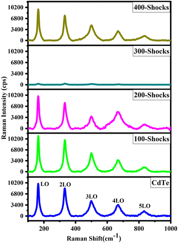
Fig. 10 shows the Raman spectra of CdTe pre- and post-shock wave exposure. In the pre-shock wave exposure, five distinct vibrational modes are identified. The first mode, observed at 164 cm−1, is attributed to the longitudinal optical (LO) phonon mode.63 Additional peaks are noted at 330, 502, 668, and 832 cm−1. These peaks correspond to the LO phonon mode's second, third, fourth, and fifth harmonics, representing higher-order lattice vibrations. Each harmonic signifies increased vibrational frequency within the crystal lattice.64,65 This detailed observation highlights the role of phonon harmonics in understanding CdTe's structural and vibrational behavior. A variation in peak intensity and the disappearance and appearance of existing peaks were observed after shock wave exposure. At 200 shock pulses, the third harmonic of the LO phonon mode showed a decrease in peak intensity, while the fourth harmonic increased. Shock wave-induced reorientation in the crystal lattice is typically associated with changes in the material's structural symmetry and bonding, which in turn cause variations in Raman intensity. These changes in atomic arrangement affect the resonance conditions, leading to fluctuations in the intensity of the Raman peaks.66 At 300 shock pulses, the LO mode did not vanish completely but showed a marked reduction in intensity, with LO peaks still discernible. In the rocksalt structure, LO modes are typically forbidden by symmetry because selection rules prevent phonons at the Brillouin zone center from being Raman active. However, these LO modes can still appear in Raman spectra due to local symmetry breaking caused by defects, strain, or disorder. These effects relax the selection rules, allowing otherwise forbidden LO modes to be detected with weaker intensity. Therefore, the presence of weak LO modes in the rocksalt phase is consistent with established physical behavior under non-ideal conditions. While the rocksalt phase is dominant, small zinc blende regions may remain at grain boundaries due to stress release, contributing to residual Raman activity. This indicates a nearly complete phase transition, with only minor traces of the zinc blende phase.67,68 This is consistent with previous reports where weak LO modes were observed even after the ZB-to-RS transition.69 The observed weakening of Raman peaks is primarily due to lattice distortion induced by shock waves, where rapid compression disrupts the crystal structure. This disruption can break bonds, reduce symmetry, and modify vibrational modes, leading to the suppression of Raman activity. A diminished LO signal does not contradict the occurrence of a phase transition; rather, it supports and confirms the transformation from the zincblende to the rocksalt structure.70 Furthermore, the disappearance of the 5LO peak at 300 shock pulses, was observed indicates a significant breakdown of long-range order characteristic of the zinc-blende structure. This higher-order mode is particularly sensitive to structural coherence, and its absence strongly supports the occurrence of a phase transition to the rocksalt phase. Such phase transition under high pressure is consistent with findings reported by Saqib et al.71 At 400 shock pulses, the LO phonon mode reappeared, which had previously disappeared. This reappearance of the 5LO peak and retention of Raman intensity of LO modes indicates a recovery or alteration in the material's vibrational structure, demonstrating that the rocksalt structure reverted to the zincblende structure. The observations highlight the reversible nature of structural transitions under acoustic shock wave exposure.
 |
| | Fig. 10 Raman spectra of CdTe pre- and post-shock wave exposure. | |
Optical analysis
UV-vis diffuse reflectance spectroscopy (DRS).
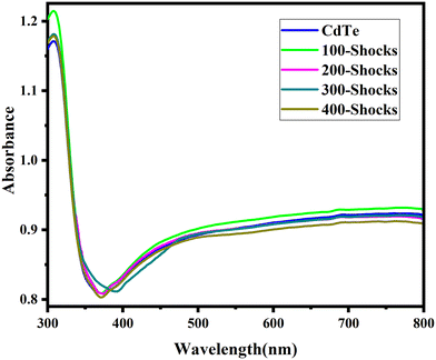
Fig. 11 represents the UV-vis DRS spectra of CdTe pre- and post-shock wave exposure. The absorption edge for CdTe, pre-shock wave exposure, was initially observed at 370.4 nm. However, notable shifts in the absorption edge were detected for post-shock wave exposure. At 100 shock pulses, the absorption edge shifted slightly, moving to 371.1 nm. When shock pulses increase to 200, the absorption edge undergoes a further shift, reaching 374.1 nm. For 300 shock pulses, a significant shift was observed, with the absorption edge shifted to 391.2 nm, which indicates the changes in the electronic structure. Interestingly, when the number of shock pulses was increased to 400, the absorption edge shifted back to 370.9 nm, which is almost close to the pre-shock wave exposure, indicating a potential reconstructable or reversal of optical behavior under acoustic shock waves. When CdTe is subjected to shock waves, both redshift and blueshift in the absorption edge were observed. A redshift occurs at 100, 200, and 300 shock pulses. Blueshift was observed at 400 shock pulses due to the changes in lattice structure caused by the shock-induced distortions.72 These shifts in the absorption edge highlight CdTe's acoustic shock wave response by varying numbers of shock pulses, suggesting potential alterations in its electronic structure.
 |
| | Fig. 11 UV-vis DRS spectra of CdTe pre- and post-shock wave exposure. | |
The absorbance spectrum was analyzed, and a Tauc plot was constructed to determine the bandgap, illustrating the difference between the valence and conduction bands. The bandgap of CdTe pre- and post-shock wave exposure was calculated. This was achieved by extrapolating the linear region of the Tauc plot to the x-axis. The energy bandgap of pre- and post-shock wave exposure samples was then obtained through the Tauc equation. The results reveal the effect of shock wave exposure on CdTe electronic properties, and the following equation was used to calculate the bandgap,
whereas “
α” stands for the absorption coefficient,
hν is the photon energy,
A is a constant, and ‘
n’ takes values of 1/2 for indirect and 2 for direct transitions. The observed linear dependence between (
αhν)
n and
hν was found to hold for
n = 2, corresponding to direct transitions since CdTe is a semiconducting material.
73 This relationship was used to extract the bandgap value from the Tauc plot.
Fig. 12 shows the Tauc plot of CdTe pre- and post-shock wave exposure.
 |
| | Fig. 12 Tauc plot of CdTe pre- and post-shock wave exposure. | |
The initial bandgap of CdTe pre-shock wave exposure was 3.31 eV. When CdTe was subjected to shock waves, the bandgap progressively changed with the number of shock pulses. After 100 shock pulses, the bandgap slightly decreased to 3.28 eV. At 200 shock pulses, it further reduced to 3.26 eV, gradually decreasing. A significant shift occurred at 300 shock pulses, where the bandgap dropped to 3.16 eV, supporting the phase transition from zinc blende to rock salt structure. Surprisingly, at 400 shock pulses, the bandgap increased to 3.30 eV and retained its initial pre-shock wave exposure value. The bandgap gradually decreased at 100, 200, and 300 shock pulses, with the most significant reduction occurring at 300 shock pulses. The variation in bandgap is attributed to shock wave-induced lattice compression, which leads to either contraction or expansion in the lattice.74 As the crystal lattice contracts, the atomic spacing is reduced, enhancing the overlap between electronic orbitals. This increased overlap facilitates electron transitions between the valence and conduction bands. Shock wave-induced compressive stress, which causes lattice contraction, increases defect density and lattice distortions, generating localized states near the band edges. These defects primarily form band tails (Urbach tails) and significantly narrow the band gap by enabling lower-energy electronic transitions. Consequently, the localization of band tails forms between the valence and conduction bands.75 These band tails are localized electronic states resulting from structural disorder and lattice defects, which reduce the energy gap by creating intermediate states. This leads to a lower conduction band and an upward shift of the valence band, causing the bandgap to narrow. This narrowing of bandgap is directly linked to a decrease in lattice parameters and unit cell volume, confirmed through Rietveld's refinement of XRD data, which provides precise insights into atomic arrangements and lattice contractions.76–78 The more significant change observed at 300 shock pulses is a result of the phase transition, which alters the material's electronic structure. At 400 shock pulses, the bandgap increased due to shock wave-induced lattice expansion. Shock wave-induced lattice expansion introduces lattice distortion, increasing atomic spacing and reducing orbital overlap. This reduction narrows the bandwidth of electronic states, increasing the energy difference between the valence and conduction bands and resulting in a wider bandgap.79 These changes, confirmed by increased lattice parameters and unit cell volume through Rietveld refinement of XRD data, validate the impact of lattice expansion on electronic properties.80–82 Shock waves reduce or delocalize the band tail by restructuring the crystal lattice and decreasing defect density. The intense pressure and temperature cause dynamic recrystallization, which repairs disordered regions and anneals out localized states near the band edges. This process narrows the band tails, reduces electronic disorder, and increases the band gap by restoring a more ordered crystal structure.83,84Fig. 13 shows the mechanism of shock-induced variation in bandgap in CdTe. Overall, these observations indicate that the shock wave-induced changes in the bandgap support the phase transition at 300 shock pulses from the zinc blende to the rock salt structure. At 400 shock pulses, the initial bandgap value is almost close to the pre-shock wave exposure value, confirming the restoration of the rock salt structure to the zinc blende structure and the reconstructable phase transition. These findings highlight both the alteration and reversibility of optical properties, which are crucial for tuning optical properties under acoustic shock waves. Fig. 14 shows the variation plot of bandgap vs. lattice parameters and bandgap vs. unit cell volume against the number of shock pulses. Fig. 15 represents the bandgap alignment of CdTe pre- and post-shock wave exposure.
 |
| | Fig. 13 Mechanism of shock wave-induced variation in the bandgap. | |
 |
| | Fig. 14 Variation plot of bandgap, unit cell volume, and lattice parameters against a number of shock waves (a) bandgap vs. lattice parameters and (b) bandgap vs. unit cell volume. | |
 |
| | Fig. 15 Schematic representation of bandgap alignment of CdTe pre- and post-shock wave exposure. | |
Photoluminescence (PL) spectroscopy.
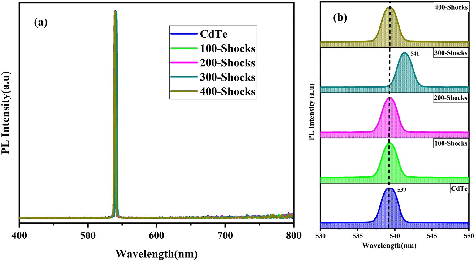
Fig. 16(a) illustrates the PL spectra of CdTe pre- and post-shock wave exposure. The emission peak of CdTe was observed at 539 nm and aligned well with reported literature values.85 The emission peak remained unchanged for 100 and 200 shock pulses. However, at 300 shock pulses, the peak shifted to a higher wavelength of 541 nm, representing a redshift. For 400 shock pulses, the peak returned to its original position at 539 nm, represented as a blue shift. Fig. 16(b) shows the zoomed version of the PL spectra. Both redshift and blueshift phenomena were observed in the material's emission peak by applying shock pulses to CdTe. When a shock wave is applied to a material, it induces lattice contraction, which decreases the atomic spacing and increases the orbital overlap within the crystal structure. This deformation creates localized band tails in the material's bandgap. The formation of these band tails lowers the energy required for electron transitions, facilitating non-radiative recombination. As a result, energy is dissipated through phonon interactions rather than photon emission. This process reduces the energy of the emitted photons, causing the emission peak to shift to a longer wavelength.86–90Fig. 17 illustrates the mechanism of the shock wave-induced emission peak shift. In contrast, the blueshift occurs due to increased mobility of the exciton's electron–hole pairs. When the material experiences strain induced by shock waves, the mobility of these charge carriers improves, making it easier for the electron and hole to recombine. This enhanced mobility promotes exciton recombination, which leads to the delocalization of the band tails, reducing their binding energy. The delocalization of the band tails leads to a shift in emission peak towards shorter wavelengths, thus resulting in a blueshift in the emission spectrum.91,92 The shift in emission peak further confirms the phase transition from zinc blende to rocksalt structure at 300 shock pulses, and reversibility of the emission peak at 400 shock pulses confirms the reconstructable or reversible phase transition from rocksalt to zinc blende structure. Fig. 18 illustrates the CIE chromaticity diagram for CdTe pre- and post-shock wave exposure. The CIE (x, y, z) chromaticity diagram is used to study color perception, hue, saturation, and color purity in light sources and materials. In contrast, X, Y, and Z represent the amounts of red, green, and blue primaries, respectively. The y-values (0.708) consistently exceeded the x-values (0.243), indicating a predominance of green color. For pre-shock wave exposure, the green color purity was 87.86%. After 100 and 200 shock pulses, the color purity remained at 87.86%. However, when the shock pulses to 300, the color purity increased to 89.40%, attributed to a shift in the emission peak. This shift enhanced the green color intensity. After exposure to 400 shock pulses, the emission peak returned to its original position, and the color purity reverted to 87.86%. High color purity is crucial in solid-state lighting devices as it ensures high-quality color rendering and efficiency. Improved color purity allows for more precise and vibrant lighting, enhancing the performance and application potential of solid-state lighting technologies, such as LEDs.93
 |
| | Fig. 16 PL spectrum (a) PL spectra of CdTe pre- and post-shock wave exposure (b) zoomed version of PL spectra. | |
 |
| | Fig. 17 Mechanism of shock wave-induced emission peak shift. | |
 |
| | Fig. 18 CIE (x, y) chromaticity diagram of CdTe pre- and post-shock wave exposure. | |
Morphological analysis
Field-emission scanning electron microscopy (FESEM).
Fig. 19 represents the FE-SEM image of CdTe pre- with EDX spectrum and post-shock wave exposure. A layered morphology was observed for CdTe pre-shock wave exposure. This morphology remained intact at 100 and 200 shock pulses, indicating that the material morphology was not significantly affected by the shock waves at these levels of shock pulses. In semiconductors, a layered morphology enhances charge transport by facilitating carrier movement, reducing recombination, and improving charge separation. It also promotes directional charge transport, which is crucial for efficient energy conversion in solar cells. The high surface area and unique interlayer spacing benefit charge transfer, ion diffusion, and electron mobility, contributing to more efficient carrier movement and boosting solar cell performance.
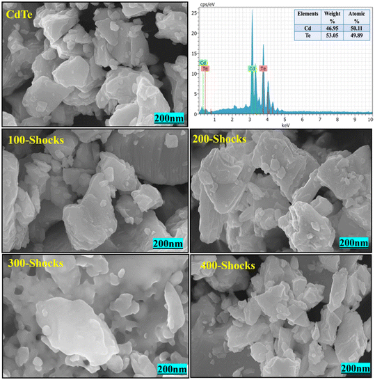 |
| | Fig. 19 FE-SEM image of CdTe pre- and post-shock wave exposure with EDX spectrum. | |
However, when the number of shock pulses increased to 300, a noticeable morphological change was observed due to shock wave-induced dynamic recrystallization.94 Shock waves induce a molten state through rapid superheating above the equilibrium melting point. This results in a premelting process where the material enters an unstable molten-like phase, followed by rapid cooling. During cooling, atoms crystallize at higher energy sites due to insufficient time to reach lower-energy configurations, initiating dynamic recrystallization and structural transitions. CdTe has a lower thermal conductivity of 6.2 W m m−2 K−1 and diffusivity of 1.4 × 10⁻⁷ m2 s−1,95 making it more susceptible to this process due to its slower heat dissipation. Morphological changes occur as the material transitions from a solid to a molten state and returns. This is influenced by thermal conductivity; due to low thermal conductivity prolongs local heating, facilitating premelting and subsequent dynamic recrystallization. The transient pressure and rapid thermal fluctuations play a crucial role in driving these changes.96 Interestingly, at 400 shock pulses, the morphology reverted to its original layered form, indicating a reconstructable phase transition driven by shock wave induced dynamic recrystallization. These, enhanced by latent heat absorption and release, stabilize the structure while modifying predominant peak intensities, suggesting shifts in orientation or crystallinity.97–99 During this recovery, the rocksalt structure reverts to the zincblende phase, and XRD results also show that the peak intensities return to their original form, confirming the restoration of the initial crystalline structure, which is the zincblende structure. The morphology change at 300 shock pulses further confirms the phase transition from zincblende to rocksalt structure. At 400 shock pulses, the retained morphology confirms the reconstructable phase transition from rocksalt to the zincblende structure. Fig. 20 illustrates the 2D surface profile of CdTe pre- and post-shock wave exposure. The 2D surface profile images reveal that with CdTe, 100, and 200 shock pulses, layer morphology with distinct sharp edges is visible. However, at 300 shock pulses, the sharp edges disappear, confirming the occurrence of dynamic recrystallization. By 400 shock pulses, the material's morphology shows signs of recovery, with sharp edges reappearing, suggesting a regaining of the original layered structure. The ability of shock-induced dynamic recrystallization to restore the morphology suggests that the shock wave treatment is an efficient method to tune the material's properties. It is critical for its application, such as in solar cells or other electronic devices.
 |
| | Fig. 20 2D surface profile of CdTe pre- and post-shock wave exposure. | |
Conclusion
This work provides valuable insights into the behavior of structural, optical, and morphological properties of CdTe under acoustic shock wave exposure. XRD and Raman spectroscopy results reveal that CdTe undergoes a phase transition from cubic-zincblende to cubic-rocksalt at 300 shock pulses, with a reconstructable nature of the phase transition at 400 shock pulses, and cubic-rocksalt restored to cubic-zincblende. This was further confirmed through Rietveld refinement, which supported the shift in crystallographic structure and enabled the calculation of lattice constants and unit cell volume. The reconstructable phase transition indicates the potential for tuning CdTe's properties under controlled acoustic shock wave exposure. Optical analysis showed a reduction in the bandgap at 300 shock pulses, indicating a change in CdTe's electronic structure. However, after 400 shock pulses, the bandgap returned to its original pre-shock wave value, highlighting the material's ability to recover its original electronic properties. PL emission also reflected this recovery, which shifted at 300 shock pulses but returned to its original position at 400 shock pulses, further supporting the reconstructable phase transition. Additionally, the color purity was calculated for CdTe pre- and post-shock wave exposure; the color purity tends to increase at 300 shock pulses and is reduced for 400 shock pulses, it returns to the original value. It shows that acoustic shock waves are capable of tuning the color purity of the sample. FE-SEM images reveal that initially, CdTe obtained layered morphology, at 100 and 200 shock pulses, it remained the same, at 300 shock pulses morphological changes were observed, which were restored at 400 shock pulses, due to dynamic recrystallization which reinforced the reconstructable phase transition, overall, dynamic recrystallization plays a major role in a reconstructable phase transition. These findings highlight that acoustic shock waves can significantly induce controlled structural modifications in CdTe, enhancing its properties without permanent degradation. This approach may improve the stability and efficiency of solar cells, with the potential to reverse phase transitions and restore material characteristics. Addressing degradation pathways is crucial for ensuring long-term reliability in CdTe-based devices.
Data availability
Data will be made available on request.
Author contributions
F. I. M. B. – methodology, investigation, data curation, writing – original draft, writing and editing, S. O – formal analysis, R. S. K. helped with the data processing and funding acquisition, P. K – formal analysis, S. A. M. B. D – conceptualization, supervision, investigation, writing review and editing, I. K – formal analysis, writing review and editing, funding acquisition. All the authors discussed the results and commented on the manuscript.
Conflicts of interest
The authors declare no conflict of interest regarding the publication of this paper.
Acknowledgements
The authors would like to thank TNSCST for their support through the RFRS scheme (TNSCST-13301/RFRS/PS/VM/2023-2024) as well as Sacred Heart College (Autonomous) for the Abraham Panampara Research Fellowship (APRF/06/2022/03). This research was supported by the Brain Pool program, funded through the National Research Foundation of Korea (RS-2023-00219593) and grant number RS-2025-00557769. The authors express their sincere appreciation to the Ongoing Research Funding program (ORF-2025-142), King Saud University, Riyadh, Saudi Arabia.
References
- T. Ju, L. Yang and S. Carter, Thickness dependence study of inorganic CdTe/CdSe solar cells fabricated from colloidal nanoparticle solutions, J. Appl. Phys., 2010, 107, 104311–110431 CrossRef.
- X. Wu, High-efficiency polycrystalline CdTe thin-film solar cells, Sol. Energy, 2004, 77, 803–814 CrossRef CAS.
- Q. Tang, J. Hui Yang, Z. Pan Liu and X. Gao Gong, Directly Determining the Interface Structure and Band Offset of a Large-Lattice-Mismatched CdS/CdTe Heterostructure, Chin. Phys. Lett., 2020, 37, 096802–096809 CrossRef CAS.
- M. A. Green, Learning experience for thin-film solar modules: First Solar, Inc. case study, Progr. Photovolt.: Res. Appl., 2011, 19, 498–500 CrossRef.
- I. V. Fisher, S. R. Cohen, A. Ruzin and D. Cahen, How Polycrystalline Devices Can Outperform Single-Crystal Ones: Thin Film CdTe/CdS Solar Cells, Adv. Mater., 2004, 16, 879–883 CrossRef.
- J. Kang, E. I. Parsai, D. Albin, V. G. Karpov and D. Shvydka, From photovoltaics to medical imaging: Applications of thin-film CdTe in x-ray detection, Appl. Phys. Lett., 2008, 93, 223507–223511 CrossRef.
- A. Rios Flores, R. C. Rodriguez, J. L. Pena, N. Romeo and A. Bosio, Characterization of CdTe films with in situ CdCl2 treatment grown by a simple vapor phase deposition technique, Appl. Surf. Sci., 2009, 255, 7012–7016 CrossRef.
- X. Wang, Y. Xu, H. Zhu, R. Liu, H. Wang and Q. Li, Crystalline Te nanotube and Te nanorods-on-CdTe nanotube arrays on ITO via a ZnO nanorod templating-reaction, CrystEngComm, 2011, 13, 2955–2960 RSC.
- B. Luo, Y. Deng, Y. Wang, M. Tan, L. Cao and W. Zhu, Fabrication and growth mechanism of zinc blende and wurtzite CdTe nanowire arrays with different photoelectric properties, CrystEngComm, 2012, 14, 7922–7928 RSC.
- B. M. Basol, Application of electrochemical deposition techniques to thin film solar cell processing, Proc. SPIE, 2011, 8110, 81100–81110 CrossRef.
- A. Shah, P. Torres, R. Tscharner, N. Wyrsch and H. Keppner, Photovoltaic technology: the case for thin-film solar cells, Science, 1999, 285, 692–698 CrossRef CAS PubMed.
- K. M. Katubi, F. M. Alzahrani, D. Ali and S. Alarifi, Dose- and duration dependent cytotoxicity and genotoxicity in human hepatocarcinoma cells due to CdTe QDs exposure, Hum. Exp. Toxicol., 2019, 38, 914–926 CrossRef CAS.
- M. Gloeckler, I. Sankin and Z. Zhao, CdTe Solar Cells at the Threshold to 20% Efficiency, IEEE J. Photovolt., 2013, 3, 1389–1394 Search PubMed.
- E. Saucedo, V. Corregidor, L. Fornaro, A. Cuna and E. Dieguez, CdTe polycrystalline films for X-ray digital imaging applications, Thin Solid Films, 2005, 471, 304–309 CrossRef CAS.
- S. Mnasri, S. AbdiBen Nasrallah, N. S. fina, N. Bouarissa and M. Said, Electronic, lattice vibration and mechanical properties of CdTe, ZnTe, MnTe, MgTe, HgTe, and their ternary alloys, Semicond. Sci. Technol., 2009, 24, 095008–095016 CrossRef.
- A. Lobo, H. Borchert, D. V. Talapin, H. Weller and T. Moller, Surface oxidation of CdTe nanocrystals A high-resolution core-level photoelectron spectroscopy study, Colloids Surf. A: Physicochem. Eng. Asp., 2006, 286, 1–7 CrossRef CAS.
- J. C. Flanagan and M. Shim, Enhanced Air Stability, Charge Separation, and Photocurrent in CdSe/CdTe Heterojunction Nanorods by Thiols, J. Phys. Chem. C, 2015, 119, 20162–20168 CrossRef CAS.
- J. Li, J. Gayles, N. Kioussis, Z. Zhang, C. Grein and F. Aqariden, Ab Initio Studies of the Unreconstructed Polar CdTe (111) Surface, J. Electron. Mater., 2012, 41, 2745–2755 CrossRef CAS.
- S. Velumani, X. Mathew, P. J. Sebastian, S. K. Narayandass and D. Mangalaraj, Structural and optical properties of hot wall deposited CdSe thin films, Sol. Energy Mater. Sol. Cells, 2003, 76, 347–358 CrossRef CAS.
- C. Hsin, J. Liu and J. H. Wang, Spray-Pyrolyzed Thin Film CdSe Photoelectrochemical Cells, J. Electrochem. Soc., 1982, 129, 719–722 CrossRef.
- C. M. Shena, X. G. Zhang and H. L. Li, Influence of different deposition potentials on morphology and structure of CdSe films, Appl. Surf. Sci., 2005, 240, 34–41 CrossRef.
- K. N. Shreekanthan, B. V. Rajendra, V. B. Kasturi and G. K. Shivakumar, Growth and characterization of semiconducting cadmium selenide thin films, Cryst. Res. Technol., 2003, 38, 30–33 CrossRef CAS.
- Y. Choi, M. Seol, W. Kim and K. Yong, Chemical Bath Deposition of Stoichiometric CdSe Quantum Dots for Efficient Quantum-Dot-Sensitized Solar Cell Application, J. Phys. Chem. C, 2014, 118, 5664–5670 CrossRef CAS.
- F. Bai, K. Bian, X. Huang, Z. Wang and H. Fan, Pressure-Induced Nanoparticle Phase Behavior, Property, and Applications, Chem. Rev., 2018, 119, 7673–7717 CrossRef.
- Z. Su, W. L. Shaw, Y. Run Miao, S. You, D. D. Dlott and K. S. Suslick, Shock wave chemistry in a metal-organic framework, J. Am. Chem. Soc., 2017, 139, 4619–4622 CrossRef CAS.
- Z. Dehghani, S. Nezamdoost, A. Vejdani Noghreiyan and M. Nadafan, The influence of γ-irradiation on molecular structure and mass attenuation coefficients of γ-Al2O3 nanoparticles, AIP Adv., 2023, 13, 035120–035125 CrossRef CAS.
- A. Sivakumar, L. Dai, S. S. J. Dhas, S. A. M. B. D. Sathiyadhas, V. Muthuvel, R. S. Kumar and A. I. Almansour, Acoustic shock wave recovery experiments on cubic zinc sulfide nanoparticles for electrical and magnetic switches applications, Ceram. Int., 2024, 50, 7418–7430 CrossRef.
- A. Sivakumar, L. Dai, S. S. J. Dhas, S. A. M. B. Dhas, K. K. Bharathi, R. S. Kumar and A. I. Almansoure, Experimental demonstration of acoustic shockwave- induced solid-state morphological transformation from irregular to rod shape: a case study of L-tyrosine, CrystEngComm, 2024, 26, 1199–1205 RSC.
- B. John and S. Varadharajaperumal,
et al.
, TEPES, 2022, 2, 180–196 CrossRef.
- S. Ranjan Bera and S. Saha, Fabrication and Characterization of Zn-doped CdTe nanoparticles-based Dye-sensitized solar cells, IOSR Journal of Electrical and Electronics Engineering, 2016, 11, 11–18 Search PubMed.
- I. M. Dharmadasa, P. A. Bingham, O. K. Echendu, H. I. Salim, T. Druffel, R. Dharmadasa, G. U. Sumanasekera, R. R. Dharmasena, M. B. Dergacheva, K. A. Mit, K. A. Urazov, L. Bowen, M. Walls and A. Abbas, Fabrication of CdS/CdTe-Based Thin Film Solar Cells Using an Electrochemical Technique, Coatings, 2014, 4, 380–415 CrossRef.
- S. Singh, R. Kumar and K. N. Sood, Structural and electrical studies of thermally evaporated nanostructured CdTe thin films, Thin Solid Films, 2010, 519, 1078–1081 CrossRef CAS.
- J. A. Rios Gonzalez, R. Mis Fernandez, E. Camacho Espinosa, I. Riech, E. Menendez Proupin, M. A. Flores, W. Orellana and J. L. Pena, Inducing a level inside of CdTe bandgap doping with Sn using a co-sublimation technique by CSS, Mater. Sci. Semicond. Process., 2020, 107, 104836–104842 CrossRef CAS.
- C. Yamcicier and C. Kurkcu, A study of structural, electronic, elastic, phonon properties, and transition mechanism of wurtzite CdTe under high-pressure, Solid State Sci., 2020, 105, 106209–106219 CrossRef CAS.
- R. J. Nelmes, M. I. McMahon, N. G. Wright and D. R. Allan, Observation of a high-pressure cinnabar phase in CdTe, Phys. Rev. B: Condens. Matter Mater. Phys., 1993, 48, 1314–1317 CrossRef CAS PubMed.
- A. Sivakumar, D. Lidong, S. S. J. Dhas, S. A. M. B. Dhas, M. Vijayan, I. Kim, R. S. Kumar and A. I. Almansour, Acoustic shock wave-induced short-range ordered graphitic domains in amorphous carbon nanoparticles and correlation between magnetic response and local atomic structures, Diamond Relat. Mater., 2024, 141, 110587–110609 CrossRef.
- A. Sivakumar, D. Lidong, S. S. J. Dhas, S. A. M. B. Dhas, R. S. Kumar and A. A. N. Raj, Acoustic shock wave induced chemical reactions–A case study of NaCl single crystal, J. Mol. Struct., 2024, 1312, 138490–138498 CrossRef.
- A. Sivakumar, D. Lidong, S. A. Martin Britto Dhas, R. Suresh Kumar, V. Thangavel and V. N. Vijayakumar, Assessment of acoustic shock wave resistance of SiO2 (α-cristobalite): A potential material for aerospace and defense industry applications, Ceram. Int., 2024, 50, 17011–17019 CrossRef.
- A. I. Khudiar, M. Zulfequar and Z. H. Khan, Influence of cadmium concentration on the optical and structural properties of cadmium selenide thin films, Mater. Sci. Semicond. Process., 2012, 15, 536–542 CrossRef CAS.
- O. Portillo Moreno, G. Abarca Avila, J. R. Cerna, J. Hernandez Tecorralco, M. Chavez Portillo, J. Martinez Juarez, R. Lozada Morales and O. Zelaya Angel, Characterization of Chemical Bath Deposited CdS, CdSe and PbS, J. Mater. Eng., 2011, 1, 692–704 Search PubMed.
- L. Wang, R. Nughays, X. Song, T. Bian, M. N. Hedhili, J. Yin, O. M. Bakr and O. F. Mohammed, Crystallographic orientation-dependent photo-response of planar cadmium telluride X-ray detectors, Cell Reports Physical, Science, 2020, 4, 101723–101736 Search PubMed.
- V. Jayaram, A. Gupta and K. P. J. Reddy, Investigation of strong shock wave interactions with CeO2 ceramic, J. Adv. Ceram., 2014, 3, 297–305 CrossRef CAS.
- A. A. Bunaciu, E. G. Udristioiu and H. Y. Aboul-Enein, X-Ray Diffraction: Instrumentation and Applications, Crit. Rev. Anal. Chem., 2015, 45, 289–299 CrossRef CAS PubMed.
- S. Rui Sun and Y. Hui Dong, First-principles study of the phase transition of HgS from cinnabar to rocksalt structure under high pressure, Phys. Rev. B: Condens. Matter Mater. Phys., 2005, 72, 174101–174109 CrossRef.
- C. Rodenkirchen, M. Cagnoni, S. Jakobs, Y. Cheng, J. Keutgen, Y. Yu, M. Wuttig and O. Cojocaru-Miredin, Employing Interfaces with Metavalently Bonded Materials for Phonon Scattering and Control of the Thermal Conductivity in TAGS-x Thermoelectric Materials, Adv. Funct. Mater., 2020, 30, 1910039–1910049 CrossRef CAS.
- A. Onodera, High pressure transition in cadmium telluride, Rev. Phys. Chem. Japan, 1970, 39, 78–92 Search PubMed.
- A. O. Adeniyi, M. Kunz, E. Stavrou and Y. Yao, High-enthalpy crystalline phases of cadmium telluride, Phys. Rev. Res., 2020, 2, 033072–033079 CrossRef CAS.
- F. I. M. Bincy, S. Oviya, R. S. Kumar, P. Kanappan, I. Kim and S. A. M. B. Dhas, Acoustic shock wave-induced reversible phase transition (rhombohedral to hexagonal) of bismuth telluride, J. Mater. Sci., 2024, 59, 7044–7059 CrossRef CAS.
- A. Sivakumar, A. Rita, S. S. J. Dhas, K. P. J. Reddy, R. S. Kumar, A. I. Almansour, S. Chakraborty, K. Moovendaran, J. Sridhar and S. A. M. B. Dhas, Dynamic shock wave driven simultaneous crystallographic and molecular switching between α-Fe2O3 and Fe3O4 nanoparticles – a new finding, Dalton Trans., 2022, 51, 9159–9166 RSC.
- A. Sivakumar, D. Lidong, S. S. J. Sahaya Jude Dhas, S. A. Martin Britto Dhas, S. Laha and R. Suresh Kumar, Acoustic Shock Wave-Induced Solid-State Fusion of Nanoparticles: A Case Study of the Conversion of One-Dimensional Rod Shape into Three-Dimensional Honeycomb Nanostructures of CdO for High- Performance Energy Storage Materials, Inorg. Chem., 2024, 63, 576–592 CrossRef.
- Z. Y. Liu, J. Li, J. F. Zhang, J. Li, P. T. Yang, S. Zhang, G. F. Chen, Y. Uwatoko, H. X. Yang, Y. Sui, K. Liu and J.-G. Cheng, Quasi-one-dimensional superconductivity in the pressurized charge-density-wave conductor HfTe3, npj Quantum Mater., 2021, 6, 90–102 CrossRef CAS.
- D. F. Zhi, B. Wen, Y. Sun, H. Xiang and Y. Zhou, Theoretical prediction on thermal and mechanical properties of high entropy (Zr0.2Hf0.2Ti0.2Nb0.2Ta0.2) C by deep learning potential, J. Mater. Sci. Technol., 2020, 43, 168–174 CrossRef.
- A. Onodera, High pressure transition in cadmium telluride, Rev. Phys. Chem. Japan, 1970, 39, 78–92 Search PubMed.
- S. Ravi, D. P. Bisen, S. Usha Shukla and B. G. Sharma, X-ray diffraction: a powerful method of characterizing nanomaterials, Recent Res. Sci. Technol., 2012, 4, 77–79 Search PubMed.
- T. Vijaya Kumar and K. V. Ramana, An effect of ball milling on microstructural parameters of nanostructured MoO3-CuO-V2O5 composite nanopowders, Int. J. Mech. Prod. Eng. Res. Dev., 2019, 9, 131–142 Search PubMed.
- M. Basak, M. Lutfor Rahman, M. Farid Ahmed, B. Biswas and N. Sharmin, The use of X-ray diffraction peak profile analysis to determine the structural parameters of cobalt ferrite nanoparticles using Debye-Scherrer, Williamson-Hall, Halder-Wagner and Size-strain plot: Different precipitating agent approach, J. Alloys Compd., 2022, 895, 162694 CrossRef CAS.
- S. Ashok Kumar, S. S. R. Inbanathan, R. B. Vignesh, D. R. Rosaline, B. R. Kamalam, A. Umar, A. A. Ibrahim, S. Akbar, S. A. Martin Britto Dhas and S. Baskoutas, Shock wave pulsed strategy on green synthesized nickel oxide nanoparticles: Structural, morphological, and electrochemical performance, Ceram. Int., 2025, 51, 4509–4520 CrossRef.
- C. O. Ehi-Eromosele, B. I. Ita and E. E. J. Iweala, Low-temperature combustion synthesis of cobalt magnesium ferrite magnetic nanoparticles effects of fuel-to-oxidizer ratio and sintering temperature, J. Sol-Gel Sci. Technol., 2015, 76, 298–308 CrossRef CAS.
- B. Azhdar, Influence of fuel-to-oxidizer ratio, potential of hydrogen and annealing temperature on the structural and optical properties of nanocrystalline MgO powders synthesized by the hydrothermal method, J. Exp. Nanosci., 2023, 18, 2276278–2276299 CrossRef.
- G. Fan, Y. Wen, B. Liu and W. Yang, An insight into the influence of crystallite size on the performances of microsized spherical Li (Ni0.5Co0.2Mn0.3) O2 cathode material composed of aggregated nanosized particles, J. Nanopart. Res., 2018, 20, 43–55 CrossRef.
- L. T. Jule, F. B. Dejene, A. G. Ali, K. T. Roro, A. Hegazy, N. K. Allam and E. El Shenawy, Wide visible emission and narrowing band gap in Cd-doped ZnO nanopowders synthesized via sol-gel route, J. Alloys Compd., 2016, 687, 920–926 CrossRef CAS.
- R. Mayahi, A. Shokuhfar and M. Reza Vaezi, Microstructure and thermodynamic analysis of nanostructured Cu-13.2%Al-4%Ni ternary system synthesized by mechanical alloying, Metall. Res. Technol., 2019, 116, 628–638 CrossRef CAS.
- M. V. Ukarande, S. Salve, O. I. Chaure, T. M. W. J. Olusola, M. Bandara, B. E. M. Furlani, M. A. K. L. Dissanayake, I. Albinsson and N. B. Chaure, Investigation of electrodeposited CdTe thin films for solar cell development, J. Mater. Sci.: Mater. Electron., 2023, 34, 1887–1897 CrossRef.
- A. Ukarande, S. M. Sonawane, S. Chaure and N. B. Chaure, Wet-electrochemical growth of CdTe layers for photovoltaic applications, J. Mater. Sci.: Mater. Electron., 2022, 33, 22456–22468 CrossRef CAS.
- J. R. Cardenas and H. Sobral, Optical Absorption Enhancement in CdTe Thin Films by Micro structuration of the Silicon Substrate, Materials, 2017, 10, 607–619 CrossRef.
- S. Farrell Turner, W. U. Reimold, M. Nieuwoudt and R. M. Erasmus, Raman spectroscopy of olivine in dunite experimentally shocked to pressures between 5 and 59 GPa, Meteorit, Planet.
Sci. J., 2005, 40, 13111327 Search PubMed.
- Z. T. Piontkowski, E. L. Runnerstrom, A. Cleri, A. McDonald, J. Ihlefeld, C. Saltonstall, J. Paul Maria and T. E. Beechem, Effects of Strain, Disorder, and Coulomb Screening on Free-Carrier Mobility in Doped Cadmium Oxide, J. Appl. Phys., 2021, 130, 195105–1951021 CrossRef CAS.
- F. S. Manciu, J. G. Salazar, A. Diaz and S. A. Quinones, Spectroscopic, microscopic, and internal stress analysis in cadmium telluride grown by close-space sublimation, Thin Solid Films, 2015, 589, 298–302 CrossRef CAS.
- H. M. Fan, Z. H. Ni, Y. P. Feng, X. F. Fan, Z. X. Shen and B. S. Zou, High-pressure Raman and photoluminescence of highly anisotropic CdS nanowires, J. Raman Spectrosc., 2007, 38, 1112–1116 CrossRef CAS.
- S. Meenakshi, S. Anitta, A. Sivakumar, S. A. M. B. Dhas and C. Sekar, Shock waves exposed α-Fe2O3 nanoparticles for electrochemical sensing of riboflavin, uric acid, and folic acid, Microchem. J., 2021, 168, 106403–106415 CrossRef CAS.
- H. Saqib, S. Rahman, D. Errandonea, R. A. Susilo, A. Jorge-Montero and P. Rodríguez-Hernández, Giant conductivity enhancement: Pressure-induced semiconductor-metal phase transition in Cd0.90Zn0.1Te, Phys. Rev. B, 2019, 99, 094109–094119 CrossRef CAS.
- N. Puri, K. Raj Gupta, N. C. Mehra, R. P. Tandon and A. K. Mahapatro, Neodymium doped bismuth telluride alloys using the chemical reflux method for thermoelectric application, Integr. Ferroelectr., 2017, 184, 9–14 CrossRef CAS.
- X. Ren, X. Yan, A. Saeed Ahmad, H. Cheng, Y. Li, Y. Zhao, L. Wang and S. Wang, Pressure-Induced Phase Transition and Band Gap Engineering in Propylammonium Lead Bromide Perovskite, J. Phys. Chem. C, 2019, 123, 15204–15208 CrossRef CAS.
- S. Kiprotich, M. O. Onani and F. B. Dejene, Effect of growth temperature on the structural, optical and luminescence properties of cadmium telluride nanoparticles, J. Mater. Sci.: Mater. Electron., 2018, 29, 6004–6011 CrossRef CAS.
- P. G. Mather, J. C. Read and R. A. Buhrman, Disorder, defects, and band gaps in ultrathin (001) MgO tunnel barrier layers, Phys. Rev. B:Condens. Matter Mater. Phys., 2006, 73, 205412–205429 CrossRef.
- Y. Kanemitsu, Y. Ishida, I. Nakada and H. Kuroda, Anomalous surface transformations in crystalline silicon induced by subpicosecond laser pulses, Appl. Phys. Lett., 1986, 48, 209–211 CrossRef CAS.
- M. Riaz, B. Ali, S. Mansoor Ali, M. Ijaz Khan, M. S. U. Sahar, M. Shahid and M. Alam, Stress-induced transformation on the cubic perovskite RbTaO3 for high-temperature applications: a DFT approach, J. Comput. Electron., 2024, 23, 483–497 CrossRef CAS.
- S. Anuchai, S. Phanichphant, D. Tantraviwat, P. Pluengphon, T. Bovornratanaraks and B. Inceesungvorn, Low-temperature preparation of oxygen-deficient tin dioxide nanocrystals and a role of oxygen vacancy in photocatalytic activity improvement, J. Colloid Interface Sci., 2018, 512, 105–114 CrossRef CAS.
- F. I. M. Bincy, S. Oviya, R. S. Kumar, P. Kannappan, S. Arumugam, I. Kim and S. A. M. B. Dhas, Investigation of bismuth selenide's structural stability and tunable bandgap under exposure to acoustic shock waves for solar cell and aerospace applications, Mech. Adv. Mater. Struct., 2024, 1–15 Search PubMed.
- M. Sharma, S. Murugavel, D. Kumar Shukla and F. M. F. de Groot, Reversal in the lattice contraction of a-Fe2O3 nanoparticles, J. Phys. Chem. C, 2018, 122, 9292–9301 CrossRef CAS.
- M. S. Schneider, B. Kad, D. H. Kalantar, B. A. Remington, E. Kenik, H. Jarmakani and M. A. Meyers, Laser shock compression of copper and copper-aluminum alloys, Int. J. Impact Eng., 2005, 32, 473–507 CrossRef.
- N. Khatun, E. G. Rini, P. Shirage, P. Rajput, S. N. Jha and S. Sen, Effect of lattice distortion on bandgap decrement due to vanadium substitution in TiO2 nanoparticles, Mater. Sci. Semicond. Process., 2016, 50, 7–13 CrossRef CAS.
- R. Sreekumar, R. Jayakrishnan, C. Sudha Kartha, K. P. Vijayakumar, S. A. Khan and D. K. Avasthi, Enhancement of band gap and photoconductivity in gamma indium selenide due to swift heavy ion irradiation, J. Appl. Phys., 2008, 103, 023709–023719 CrossRef.
- S. Oviya, F. I. M. Bincy, S. Arumugam, K. K. Bharathi, R. S. Kumar, P. Kannappan, I. Kim and S. A. M. B. Dhas, Acoustic shock wave-induced phase transition in indium selenide: tuning band gap energy for solar cell applications, CrystEngComm, 2024, 26, 2498–2510 RSC.
- E. Gharibshahi, Simulation, Synthesis and Optical Properties of Cadmium Telluride (CdTe) Semiconductor Nanoparticles, Solid State Commun., 2020, 320, 114009–114033 CrossRef CAS.
- C. Hu, X. Zeng, J. Cui, H. Chen and J. Lu, Size effects of Raman and photoluminescence spectra of CdS nanobelts, J. Phys. Chem. C, 2013, 117, 20998–21005 CrossRef CAS.
- D. Han, G. Yue, K. Wang, J. Baugh and Y. Wu, Nanovoid-related large redshift of photoluminescence peak energy in hydrogenated amorphous silicon, Appl. Phys. Lett., 2002, 80, 40–42 CrossRef CAS.
- S. P. Fu, Y. F. Chen and K. Tan, Recombination mechanism of photoluminescence in InN epilayers, Solid State Commun., 2006, 137, 203–207 CrossRef CAS.
- Z. Fang, H. He, L. Gan, J. Li and Z. Ye, Understanding the Role of Lithium Doping in Reducing Nonradiative Loss in Lead Halide Perovskites, Adv. Sci., 2018, 5, 1800736–1800742 CrossRef.
- K. D. Jons, R. Hafenbrak, R. Singh, F. Ding, J. D. Plumhof, A. Rastelli, O. G. Schmidt, G. Bester and P. Michler, Dependence of the redshifted and blue-shifted photoluminescence spectra of single InxGa1- xAs/GaAs quantum dots on the applied uniaxial stress, Phys. Rev. Lett., 2011, 107, 217402–217408 CrossRef CAS PubMed.
- J. A. Suchikova, V. V. Kidalov and G. A. Sukach, Blue shift of photoluminescence spectrum of porous InP, ECS Trans., 2010, 25, 59–64 CrossRef CAS.
- H. Zeng, G. Duan, Y. Li, S. Yang, X. Xu and W. Cai, Blue luminescence of ZnO nanoparticles based on non-equilibrium processes defect origins and emission controls, Adv. Funct. Mater., 2010, 20, 561–572 CrossRef CAS.
- Y. Fang Wu, Y. Tang Nien, Y. Jhang Wang and I. Gann Chen, Enhancement of Photoluminescence and Color Purity of CaTiO3: Eu Phosphor by Li Doping, J. Am. Ceram. Soc., 2012, 95, 1360–1366 CrossRef.
- A. Sivakumar, D. Lidong, S. S. J. Dhas, S. A. M. B. Dhas, S. Laha, R. S. Kumar and A. I. Almansour, Acoustic Shock Wave-Induced Solid-State Fusion of Nanoparticles: A Case Study of the Conversion of One-Dimensional Rod Shape into Three-Dimensional Honeycomb Nanostructures of CdO for High- Performance Energy Storage Materials, Inorg. Chem., 2024, 63, 576–592 CrossRef.
- T. K. Nideep, M. Ramya, V. P. N. Nampoori and M. Kailasnath, The size-dependent thermal diffusivity of water soluble CdTe quantum dots using dual beam thermal lens spectroscopy, Phys. E, 2020, 116, 113724–113730 CrossRef CAS.
- A. Sivakumar, S. Lidong Dai, S. J. Dhas, S. Cathrin Lims and R. S. Kumar, Acoustic shock wave-induced B1 to B2 phase transition of CdO nanoparticles: Structure-property relationship and its mechanism in thermodynamic aspects, Acta Mater., 2025, 286, 120742–120757 CrossRef.
- A. Sivakumar, D. Lidong, S. S. J. Dhas, S. A. M. B. Dhas, P. Eniya, R. S. Kumar and A. I. Almansour, Experimental Evidence
of Acoustic Shock Wave-Induced Dynamic Recrystallization: A Case Study on Ammonium Sulfate, Cryst. Growth Des., 2024, 24, 491–498 CrossRef.
- S. N. Luo and T. J. Ahrens, Shock-induced superheating and melting curves of geophysically important minerals, Phys. Earth Planet. Inter., 2004, 369, 143–144 Search PubMed.
- T. Sakai, A. Belyakov, R. Kaibyshev, H. Miura and J. J. Jonas, Dynamic and post-dynamic recrystallization under hot, cold and severe plastic deformation conditions, Prog. Mater. Sci., 2014, 60, 130 CrossRef CAS.
|
| This journal is © The Royal Society of Chemistry 2025 |
Click here to see how this site uses Cookies. View our privacy policy here. 
 b,
P.
Kannappan
a,
Ikhyun
Kim
b,
P.
Kannappan
a,
Ikhyun
Kim