
Low contact resistance in carbon nanotube devices: metal-induced gap states†
Bo
Zhang
 a,
Xiaojie
Liu
*a,
Huan
Wang
*ab,
Lifeng
Feng
*a and
Haitao
Yin
*a
a,
Xiaojie
Liu
*a,
Huan
Wang
*ab,
Lifeng
Feng
*a and
Haitao
Yin
*a
aKey Laboratory for Photonic and Electronic Bandgap Materials of Ministry of Education, School of Physics and Electronic Engineering, Harbin Normal University, Harbin, 150025, China. E-mail: wlyht@126.com; redlxj@126.com; hsdflf@163.com; Tel: +86 45188060526
bCollege of Science, Qiqihar University, Qiqihar, 161006, China. E-mail: lixueyuanwh@163.com
First published on 28th November 2024
Abstract
Designing devices with low contact resistance, especially those based on carbon-based materials, is becoming increasingly important. In this work, we investigated the electronic structure and transport properties of two-types of structures based on carbon nanotubes connecting graphene electrodes by combining density functional theory with the non-equilibrium Green's function method. The directly connected structure exhibits ohmic contact and has a lower contact resistance compared to the typical van der Waals-connected structure. Furthermore, a metal-induced gap state in the directly connected structure provides an extra transport channel, making electron travel easier. The two structures have around a 4-order-of-magnitude difference in conductance at equilibrium and a 5-order-of-magnitude difference in contact resistance at a bias voltage of 0.4 V. This work may offer basic predictions for carbon nanotube transport as well as novel concepts for designing carbon nanotube transistors.
1. Introduction
The electrical contact through which charge carriers are introduced into a semiconducting material is crucial for obtaining low power consumption and high performance in traditional Si-based devices and future two-dimensional (2D) material-based transistors. The latter is considered to be the main alternative to overcome the short channel effect that exists in Si metal-oxide–semiconductor field-effect-transistors. With the scaling down of electronic devices, contact resistance is becoming an increasingly critical component, and even becoming a dominant factor in high-performance applications. For 2D material-based devices, the high contact resistance mainly stems from the presence of a high Schottky barrier between the metal and the semiconductor.1 Unfortunately, most 2D-layered materials do not lend themselves to classical substitutional doping, which results in severe interface traps and impurities. In recent years, a variety of techniques for reducing the impact of the Schottky barrier2 have been investigated, including changing the contact location,3,4 doping or introducing defects,5–7 replacing different metal electrodes as well as the semiconducting materials,8,9 and eliminating van der Waals bonds.10–13To overcome the increasing difficulties and fundamental limitations of conventional Si-based microelectronics, carbon-based devices have been considered as potential building blocks for future nanoelectronic systems. Graphene,14–17 C60,18–20 carbon nanotubes21 or other novel all-carbon devices have been reported.22–24 Among them, carbon nanotubes (CNTs),25 as the most widely studied one-dimensional wire materials, possess various excellent mechanical and thermal properties, which make them uniquely advantageous for designing multifunctional devices or sensors and thus play an important role in the design of all-carbon devices. Due to their extremely high mobility for both electrons and holes, CNTs have more important application potential in field-effect transistors (FETs). As the scale is reduced to the sub-10 nm technology node, CNT-based FETs exhibit more outstanding characteristics than conventional Si complementary metal oxide semiconductor (CMOS) FETs.26–28 Especially when connected with graphene, CNT FETs could be scaled down to 5 nm without any significant short-channel effect, and a near or even below thermionic limit subthreshold swing value of 60 mV per decade was found.29,30
In previous studies, when using CNTs to make devices, it was more often considered that the nanotubes and graphene formed a structure with van der Waals heterojunctions.30 In fact, due to the presence of weak van der Waals bonds, the electrons face a large tunneling potential barrier so that such a structure is bound to have a large contact resistance. Thus, the development of a direct-connected device that does not rely on intermolecular forces but instead directly allows nanotubes to make covalent connections with electrodes will be extremely beneficial in terms of reducing the contact resistance and improving stability. Moreover, the unique combination of graphene's high electron mobility and CNTs’ structural versatility makes them ideal as flexible supercapacitors and high-performance batteries.31,32
In this study, a CNT was covalently bonded to two graphene electrodes to form a device known as a directly connected structure (DCS), and its transport properties were compared to those of a van der Waals heterojunction structure (VHS). The DCS exhibits ohmic contact and the metal-induced gap states (MIGs)33 in the DCS provide an extra transport pathway for electrons to flow, resulting in a lower contact resistance than that in a VHS.
2. Model and methodology
Two types of carbon nanotube devices, DCS and VHS, were constructed as shown in Fig. 1. To investigate the effect of different connections on transport, we used a semiconducting CNT quantified by the chirality vector (0,10) as an example, which served as the central scattering region for both structures. A DCS corresponds to an edge contact between the graphene electrode and the nanotube, and a VHS is a top contact. A sufficiently large vacuum layer was set in the vertical graphene direction to eliminate layer-to-layer interactions. For both structures, the atoms at the interface of the central region and the electrode were subsequently optimized using VASP34 at the level of a generalized gradient approximation,35 respectively. An internal relaxation method with a fixed lattice constant was used to ensure that the periodicity of the electrodes was preserved. Among them, the DCS model was optimized to produce a significant distortion at the graphene and nanotube interface, and the VHS model was optimized after considering the van der Waals correction with the DFT-D3 method of Grimme with a zero-damping function,36 which has a vertical distance of 3.12 Å between the CNT and graphene. This result is in general agreement with the data already reported.37,38 | ||
| Fig. 1 Schematic structures of the carbon nanotube device. (a) DCS; (b) VHS. | ||
The DCS and the VHS were built once the structural optimization of the basic unit was completed. The lattice vectors of the DCS and VHS structures are (29.84 Å, 25.00 Å, 50.68 Å) and (29.82 Å, 25.00 Å, 60.51 Å), respectively. To compare the properties of the two structures, the distance between the inner edges of the graphene buffer layers on both sides was controlled to be approximately equal, instead of using the same length of carbon nanotube. The distance between the two graphene edges is 24.85 and 23.45 Å in the DCS and the VHS, respectively, as illustrated in Fig. 1. In order to prevent direct tunneling effects, sufficiently long carbon nanotubes were chosen. The structures of DCS and VHS contain 546 and 700 atoms, respectively. Considering computational efficiency and numerical stability, the local density approximation exchange–correlation functional was adopted.39 The transport properties were investigated using the Nanodcal40 package based on the density functional theory (DFT) and the nonequilibrium Green's function (NEGF) method. A double ζ-polarized atomic orbital basis was adopted to expand the wave functions and the standard nonlocal norm-conserving pseudopotential to describe the atomic cores.41,42 The k-point sampling was set to 3 × 1 × 100 in the self-consistent calculations of the electrodes and 3 × 1 × 1 in the self-consistent calculations of the device.
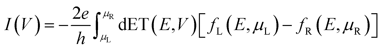
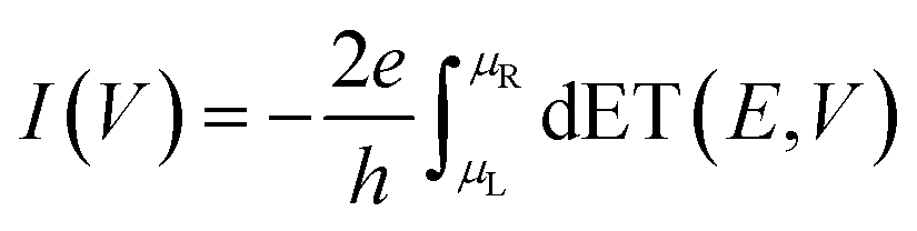
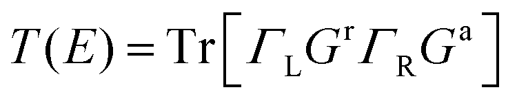
According to the NEGF theory, the current through the device can be calculated using the Landauer–Büttiker formula,43
 | (1) |
 | (2) |
 | (3) |
Here Gr(Ga) represents the retarded (advanced) Green's function of the system. ΓL/R represents the linewidth function, which describes the strength of the interaction of the central region between the electrodes. The conductance at low temperatures could be approximated as 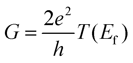 , where Ef is Fermi energy.44
3. Results and discussion
The I–V curves of the two structures were first stated, as shown in Fig. 2, where the left side of the vertical axis indicates DCS and the right vertical axis represents the current of VHS. The ohmic contact is demonstrated by the fact that the current in the DCS grows approximately proportionately to the voltage. However, the current in the VHS is very small. The conductance of the DCS structure is 4.40 × 10⁻³G0 and the VHS structure is 2.14 × 10⁻⁷G0 at equilibrium (G0 is the quantum conductance with G0 = e2/h = 3.876 × 10⁻⁵ S). At smaller bias voltages (0.4 V), the current can be on the order of microamps. In comparison, there is essentially little current in the VHS structure, which is at the picoamp level. The difference between the two structures is about four orders of magnitude. The contact resistances of DCS and VHS are 1.36 × 10⁵ Ω and 1.23 × 10¹⁰ Ω, respectively, at an operating voltage of 0.4 V. Here we consider the electrons to be ballistically transported in the nanotube, and the contact resistance is equal to half of the total resistance. The contact resistance of the DCS structure obtained here is close to that of the vertically contacted graphene/(8, 0) carbon nanotube calculated using the NEGF method.45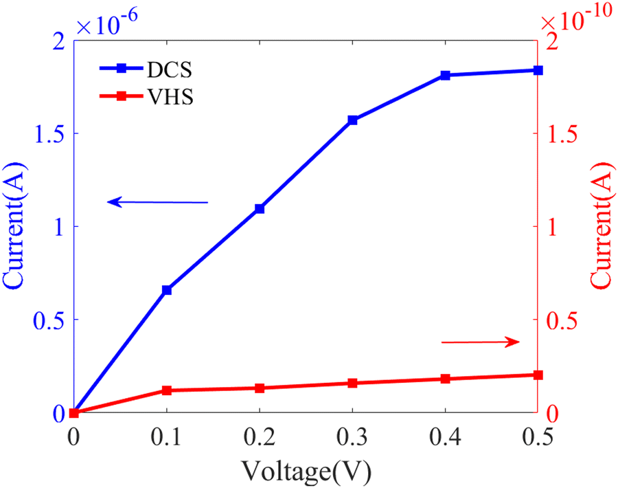 | ||
| Fig. 2 I–V curve of the CNT devices. | ||
To investigate the origin of the above current differences, we calculated the transmission spectra of the two structures at different bias voltages, as shown in Fig. 3. For the DCS, the transmission peak near Fermi energy (labeled “A”) plays a major role in the current at low bias voltages (V < 0.2 V). This peak shifts toward the lower energy direction but remains inside the bias window and therefore always contributes to the current as the bias increases. When the bias voltage is greater than 0.2 V, a gradually rising transmission peak (labeled “B”) near the Fermi energy appears, causing the increase of the current and resulting in a roughly linear I–V curve and forming a current characteristic resembling an ohmic contact. Conversely, since essentially little transmission occurs in the VHS structure, it displays an almost insulating characteristic. We further calculated the projected density of states (PDOS) of the system to account for the origin of the A and B peaks in the DCS, which are generated from different causes. PDOS is obtained by projecting the DOS onto the atoms and aligning them along the transport direction, as shown in Fig. 4. As for the A peak, it comes from the contribution of the valence band, which is more clearly seen in the PDOS (see Fig. 4(a)), where the electrode forms an ohmic contact with the carbon nanotube. For the individual periodic CNT that we chose for building the devices, the Fermi level is in the middle of the band gap, and its gap width is about 0.92 eV. However, after the formation of the device, the overall Fermi energy moves to a position close to the top of the valence band. The contribution of the valence band to transport forms peak A. The location where the B peak appears corresponds to the band gap in the carbon nanotube, which originates from MIGs, and it provides a transmission channel for the electrons to the extent that a transmission peak appears in the original gap in the equilibrium state, as shown in Fig. 4(b). The electrode and the carbon nanotube for the VHS structure form a Schottky barrier of 0.19 eV, exhibiting p-type semiconductor characteristics (see Fig. 4(c)). The obtained Schottky barrier is lower than that of structures with Au and Pt as electrodes, but higher than the barrier formed by Pd(100).46,47 The transmission coefficient of incident electrons with energy corresponding to the band gap of a carbon nanotube is low. At the same time, the transmission coefficient of incident electrons with energies corresponding to the conduction or valence bands is also low due to the weak van der Waals bonding between the electrode and the carbon nanotube; electrons from the electrode must enter the nanotube via the tunneling effect, resulting in a low transmission coefficient. Comparing the tunneling potential barriers at the interfaces of the two structures, Fig. 5 shows the effective potential Veff, which is defined as the sum of the electrostatic potential and the exchange–correlation potential. It is provided along the y direction (i.e., along the van der Waals heterojunction direction) for the VHS structure and along the transport direction for the DHS structure. The effective tunnel barrier height (ΦTB,eff) is defined as the minimum barrier height that an electron from the metal has to overcome if it has the same potential energy as the Veff of the CNT (ΦCNT). Clearly, in the VHS structure, there is a tunneling barrier with a height of 0.17 eV (ΦTB,eff = 0.17 eV) and a width of 3.12 Å, while in the DCS structure, the tunneling barrier disappears (ΦTB,eff = 0 eV).
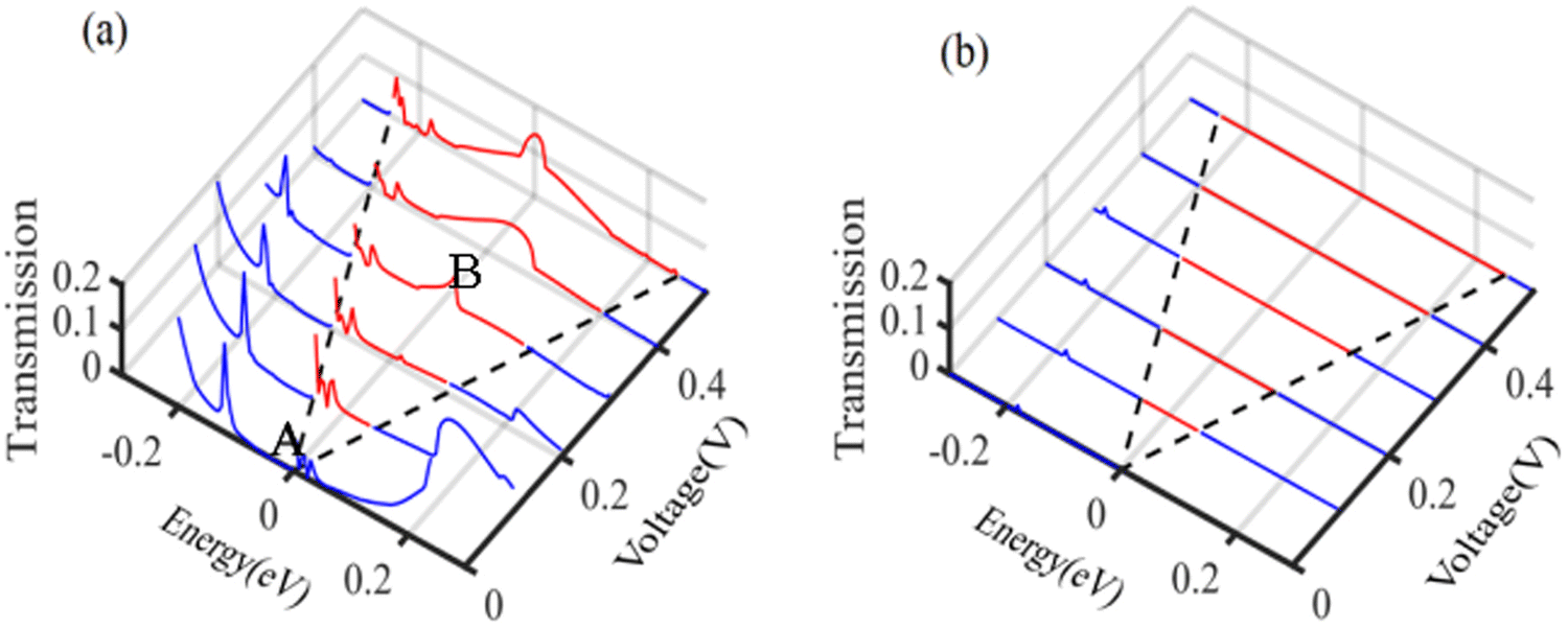 | ||
| Fig. 3 Transmission in two structures with varying bias voltages. (a) DCS; (b) VHS. | ||
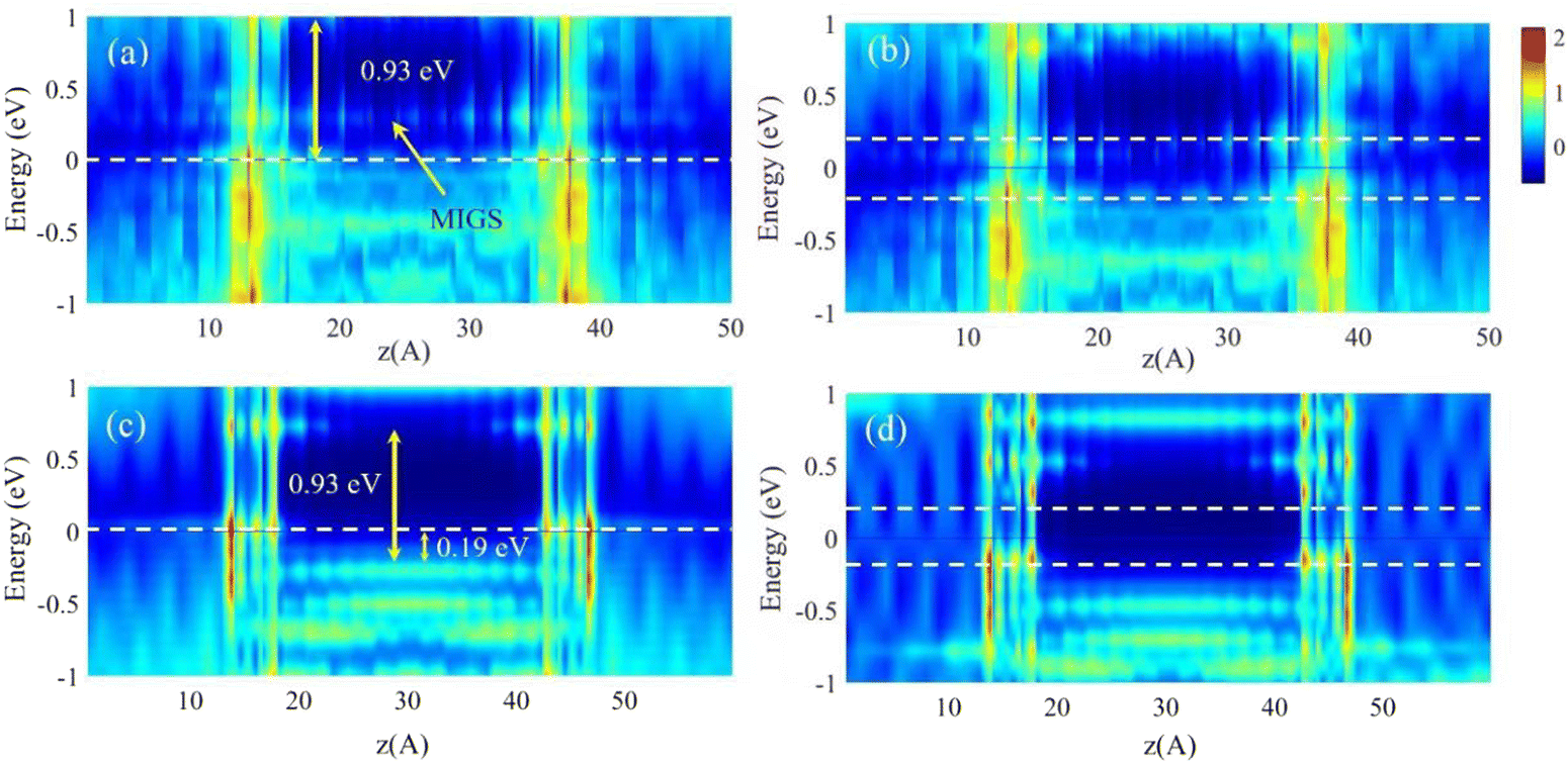 | ||
| Fig. 4 Band alignment of the two structure; (a) V = 0 V and (b) V= 0.4 V for DCS; (c) V = 0 V and (d) V= 0.4 V for VHS. | ||
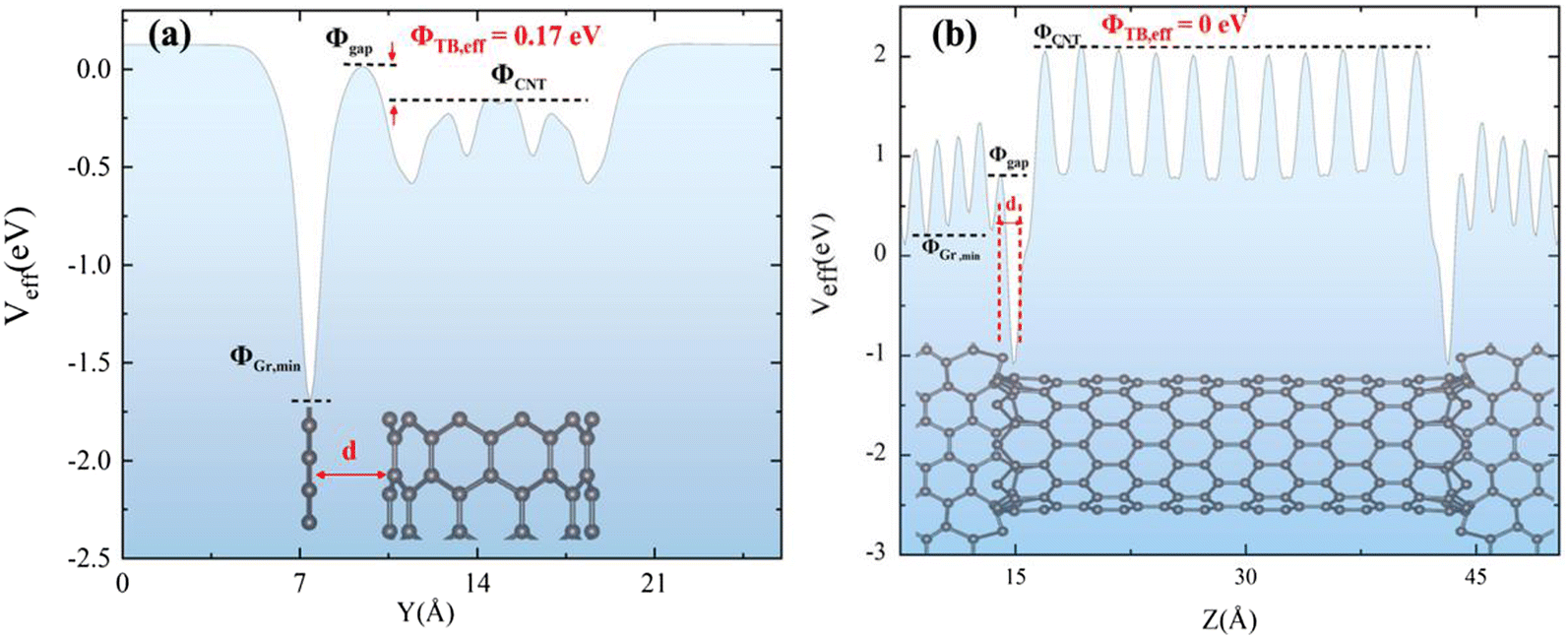 | ||
| Fig. 5 Effective potential of (a) VHS and (b) DCS. The effective tunnel barrier height (ΦTB,eff) can be calculated as the Veff difference between the vdW gap (Φgap) and CNT (ΦCNT). ΦGr;min denotes the minimum Veff in the graphene electrode. ΦTB,eff vanishes when ΦGr,min or ΦCNT is higher than Φgap. d denotes the nearest carbon–carbon atom distance between the graphene and CNT. | ||
The distinction between the two structures can also be seen by the local density of states (LDOS). Here, the energy is taken as 0.005 eV, which corresponds to peak A in the equilibrium transmission spectrum of the DCS structure. The inner edges of graphene, the outer edges of the carbon nanotubes, and the central region of the carbon nanotubes provide a large number of states in the DCS structure, as shown in Fig. 6(a). These states serve as electron transport channels, allowing electrons to pass smoothly through the junction and producing a transport peak at this energy. In contrast, the electrodes in the VHS structure are not directly attached to the central region. To enter the carbon nanotube, electrons must undergo the tunneling effect. In other words, the carbon nanotube region is essentially stateless at this energy, meaning that electrons must undergo three potential barriers, two van der Waals gaps, and one Schottky barrier when moving from the left electrode to the right electrode (see Fig. 6(c)). As a result, the transmission coefficient at this energy is almost zero, as illustrated in Fig. 6(d).
 | ||
| Fig. 6 LDOS and transmission at equilibrium. (a) LDOS and (b) transmission of DCS; (c) LDOS and (d) transmission of VHS. LDOS was calculated at an energy of 0.005 eV. | ||
As the voltage increases, the DOS in the central region moves toward lower energy. But the distance from the chemical potential of the left electrode to the top of the valence band remains constant, as shown in Fig. 4(b) and (d), showing a Fermi level pinning effect.48 This could also be reflected in the transmission spectrum (see Fig. 3), as the distance between the low-energy end of the bias window and the transmission peak contributing to the top of the valence band remains essentially constant as the bias is increased. Due to this pinning effect, the valence band top contribution to transmission for DCS structures is always inside the bias window, while for VHS structures, it is always outside the bias window. This is another reason why the latter has a much lower current than the former.
In addition, to visualize which atoms provide the MIGs state, Fig. 7 depicts the LDOS of DCS, corresponding to the peak with an energy of 0.3 eV in the transmission coefficient at 0.4 V bias. Clearly, the atoms underneath the CNT provide more states than the other parts. MIGs are generated by the contact between a metal and a semiconductor because the wave function of the metal no longer follows the boundary criteria at the interface.33 In this model, the presence of the electrodes causes the axisymmetric nature of the carbon nanotubes to be disrupted, and carbon atoms located below interact strongly with the graphene electrodes by hybridization, yielding more states for electron travel than carbon atoms at other positions. These states were also predicted in structures where graphene is in vertical contact with (8,0) carbon nanotubes using the NEGF method.49
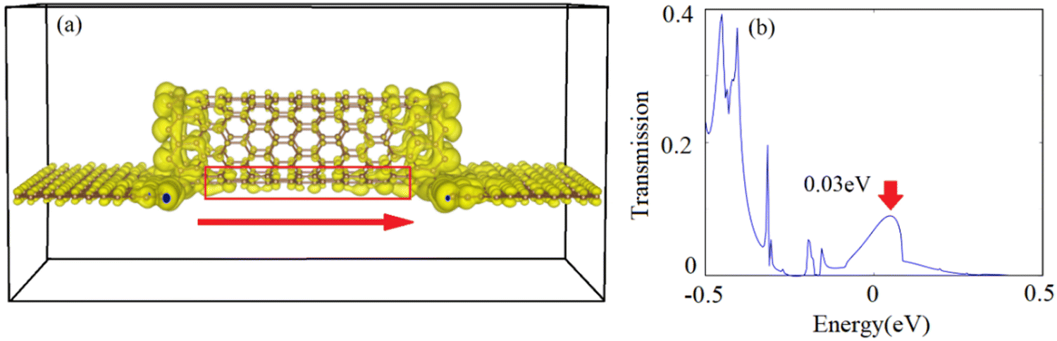 | ||
| Fig. 7 (a) LDOS at energy 0.03 eV and (b) transmission of DCS at the bias 0.4 V. | ||
Finally, we emphasize that the electronic structure of the electrode also plays an important role in the transport process. The electrons incident from the lead have their own energy–momentum distribution, as shown in Fig. 8(a), in accordance with the dispersion relationship related to the Dirac cone structure in graphene. The electrons exhibit varied transmission probabilities after scattering in the central region, as shown in Fig. 8(c). Only the central cone point has transmission at Fermi energy. At 0.3 eV, the transmission coefficient value at the cone's surface is the highest. Thus, the transmission spectrum is caused by the combined influence of the electrode and the central region, where the graphene electrode first forces the electrons to remain consistently inside the Dirac cone, and then the central region's state distribution screens these electrons a second time to create the transmission spectrum depicted in the figures.
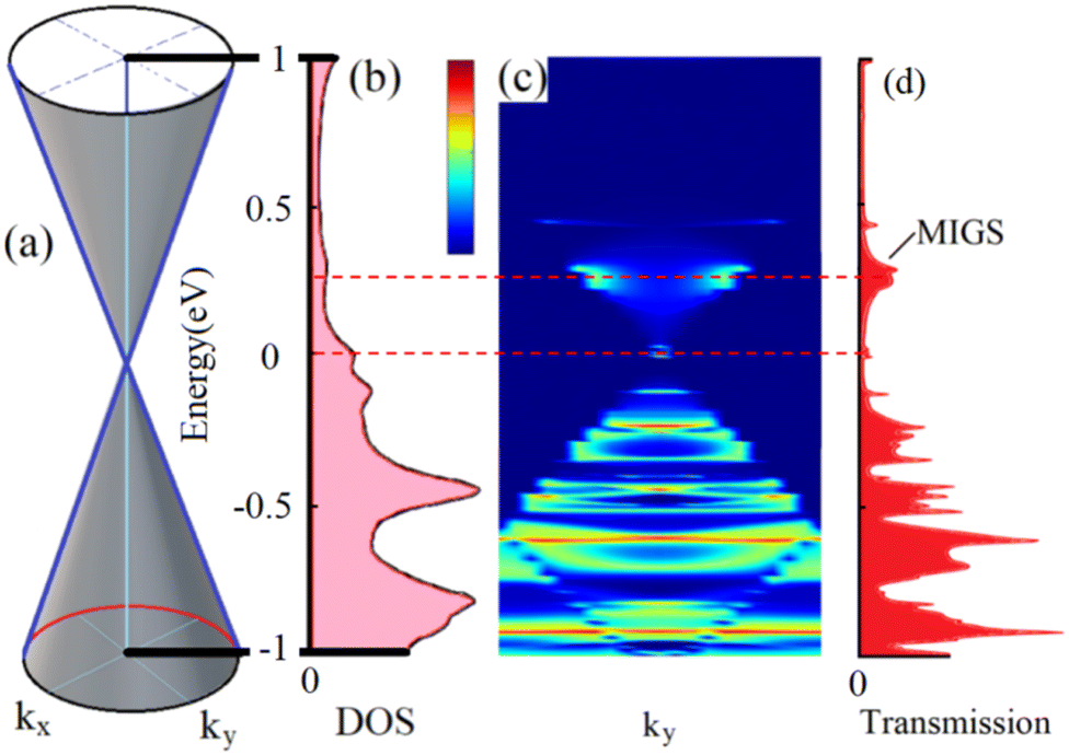 | ||
| Fig. 8 (a) Dirac cone of the graphene; (b) PDOS on CNTs; (c) transmission vs. k and energy; (d) transmission vs. energy at equilibrium, weighted average on k. | ||
4. Summary
In this study, two carbon nanotube-based devices were constructed and analyzed using the DFT-NEGF approach: one with a direct connection and the other with a van der Waals heterojunction connecting graphene electrodes. It was discovered that the transport properties of DCS and VHS differ significantly. The DCS forms an ohmic contact, where the valence band top plays a key role in transport at low bias voltages. As the bias voltage increases, the MIGs contribute more to the current. Due to the combined impact of both factors, the system's current develops linearly with bias. For VHS, the presence of a tunneling barrier, originating from the weak van der Waals connection between the electrodes and the nanotube, makes it difficult for electrons to pass through the junction, resulting in a small transmission probability. Consequently, the contact resistance of DCS is several orders of magnitude lower than that of VHS at the same voltage. This work provides ideas for obtaining carbon nanotube-based devices with low contact resistance.Data availability
All data that support the findings of this study are included within the article and any ESI.†Conflicts of interest
There are no conflicts of interest to declare.Acknowledgements
This research was supported by the Open Project of Heilongjiang Key Laboratory of Micro Nano Sensors (grant no. WNCGQJKF202107). We gratefully acknowledge HZWTECH for providing computation facilities and Li Niu for VASP calculations.References
- J. Kang, W. Liu, D. Sarkar, D. Jena and K. Banerjee, Computational study of metal contacts to monolayer transition-metal dichalcogenide semiconductors, Phys. Rev. X, 2014, 4, 031005 CAS.
- A. Allain, J. Kang and K. Banerjee, Electrical contacts to two-dimensional semiconductors, Nat. Mater., 2015, 14, 1195–1205 CrossRef CAS.
- L. Wang, I. Meric, P. Y. Huang, Q. Gao, Y. Gao, H. Tran, T. Taniguchi, K. Watanabe, L. M. Campos, D. A. Muller, J. Guo, P. Kim, J. Hone, K. L. Shepard and C. R. Dean, One-dimensional electrical contact to a two-dimensional material, Science, 2013, 342, 614–617 CrossRef CAS.
- D. Kiriya, M. Tosun, P. Zhao, J. S. Kang and A. Javey, Air-stable surface charge transfer doping of MoS2 by benzyl viologen, J. Am. Chem. Soc., 2014, 136, 7853–7856 CrossRef CAS.
- Y. F. Cong, B. R. Tao, X. Z. Lu, X. J. Liu, Y. Wang and H. T. Yin, Effect of point defects on the band alignment and transport properties of 1T-MoS2/2H-MoS2/1T-MoS2 heterojunctions, Phys. Chem. Chem. Phys., 2024, 26, 1323 Search PubMed.
- H. Li, M. Cheng, P. Wang, R. Du, L. Song, J. He and J. Shi, Reducing contact resistance and boosting device performance of monolayer MoS2 by in situ Fe doping, Adv. Mater., 2022, 34, 2200885 CrossRef CAS.
- H. Park, W. Jung, D. Kang, J. Jeon, G. Yoo, Y. Park, J. Lee, Y. H. Jang, J. Lee, S. Park, H. Yu, B. Shin, S. Lee and J. Park, Extremely low contact resistance on graphene through n-type doping and edge contact design, Adv. Mater., 2016, 28, 864–870 CrossRef CAS.
- S. M. Song, J. K. Park, O. J. Sul and B. J. Cho, Determination of work function of graphene under a metal electrode and its role in contact resistance, Nano Lett., 2012, 12, 3887–3892 CrossRef CAS.
- Y. Wang, J. C. Kim, R. J. Wu, J. Martinez, X. Song, J. Yang, F. Zhao, A. Mkhoyan, H. Y. Jeong and M. Chhowalla, van der Waals contacts between three-dimensional metals and two-dimensional semiconductors, Nature, 2019, 568, 70–74 CrossRef CAS.
- J. X. Zan, H. Wang, B. R. Tao, X. J. Liu, Y. Wang and H. T. Yin, Strong hybridization of Nb2C with MoS2: a way to reduce contact resistance, J. Phys. D: Appl. Phys., 2024, 57, 325103 CrossRef CAS.
- I. Popov, G. Seifert and D. Tománek, Designing electrical contacts to MoS2 monolayers: a computational study, Phys. Rev. Lett., 2012, 108, 156802 CrossRef.
- J. Kang, W. Liu and K. Banerjee, High-performance MoS2 transistors with low-resistance molybdenum contacts, Appl. Phys. Lett., 2014, 104, 093106 CrossRef.
- L. Gan, Y. Zhao, D. Huang and U. Schwingenschlogl, First-principles analysis of MoS2/Ti2C and MoS2/Ti2CY2 (Y = F and OH) all-2D semiconductor/metal contacts, Phys. Rev. B: Condens. Matter Mater. Phys., 2013, 87, 245307 CrossRef.
- K. S. Novoselov, A. K. Geim, S. V. Morozov, D. Jiang, Y. Zhang, S. V. Dubonos, I. V. Grigorieva and A. A. Firsov, Electric Field Effect in Atomically Thin Carbon Films, Science, 2004, 306, 666–669 CrossRef CAS PubMed.
- C. Deng, L. Lan, P. He, C. Ding, B. Chen, W. Zheng, X. Zhao, W. Chen, X. Zhong, M. Li, H. Tao, J. Penga and Y. Cao, High-performance capacitive strain sensors with highly stretchable vertical graphene electrodes, J. Mater. Chem. C, 2020, 8, 5541–5546 RSC.
- G. Sfuncia, G. Nicotra, F. Giannazzo, B. Pécz, G. K. Gueorguiev and A. Kakanakova-Georgieva, 2D graphitic-like gallium nitride and other structural selectivity in confinement at the graphene/SiC interface, CrystEngComm, 2023, 25, 5810 RSC.
- A. Kakanakova-Georgieva, G. K. Gueorguiev, D. G. Sangiovanni, N. Suwannaharn, I. G. Ivanov, I. Cora, B. Pécz, G. Nicotra and F. Giannazzo, Nanoscale phenomena ruling deposition and intercalation of AlN at the graphene/SiC interface, Nanoscale, 2020, 12, 19470 RSC.
- W. Kroto, J. R. Heath, S. C. O’Brien, R. F. Curl and R. E. Smalley, C60: Buckminsterfullerence, Nature, 1985, 318, 162–163 CrossRef.
- L. Hou, X. Cui, B. Guan, S. Wang, R. Li, Y. Liu, D. Zhu and J. Zheng, Synthesis of a monolayer fullerene network, Nature, 2022, 606, 507–510 CrossRef CAS PubMed.
- E. Meirzadeh, A. M. Evans, M. Rezaee, M. Milich, C. J. Dionne, T. P. Darlington, S. T. Bao, A. K. Bartholomew, T. Handa, D. J. Rizzo, R. A. Wiscons, M. Reza, A. Zangiabadi, N. Fardian-Melamed, A. C. Crowther, P. J. Schuck, D. N. Basov, X. Zhu, A. Giri, P. E. Hopkins, P. Kim, M. L. Steigerwald, J. Yang, C. Nuckolls and X. Roy, A few-layer covalent network of fullerenes, Nature, 2023, 613, 71–76 CrossRef CAS PubMed.
- C. G. Qiu, Z. Y. Zhang, M. M. Xiao, Y. J. Yang, D. L. Zhong and L. M. Peng, Scaling carbon nanotube complementary transistors to 5-nm gate lengths, Science, 2017, 355, 271–276 CrossRef CAS PubMed.
- L. Zhang, H. Li, Y. P. Feng and L. Shen, Diverse transport behaviors in cyclo[18] carbon-based molecular devices, J. Phys. Chem. Lett., 2022, 11, 2611–2617 CrossRef.
- B. Wang, J. Li, Y. Yu, Y. Wei, J. Wang and H. Guo, Giant tunnel magneto-resistance in graphene based molecular tunneling junction, Nanoscale, 2016, 8, 3432 RSC.
- X. F. Yang, Y. W. Kuang, Y. S. Liu, D. B. Zhang, Z. G. Shao, H. L. Yu, X. K. Hong, J. F. Feng, X. S. Chen and X. F. Wang, Carbon-based molecular devices: Fano effects controlled by the molecule length and the gate voltage, Nanoscale, 2016, 8, 15712 RSC.
- S. Iijima, Helical microtube of graphene carbon, Nature, 1991, 354, 56–58 CrossRef CAS.
- G. S. Tulevski, A. D. Franklin, D. Frank, J. M. Lobez, Q. Cao, H. Park, A. Afzali, S. J. Han, J. B. Hannon and W. Haensch, Toward high-performance digital logic technology with carbon nanotubes, ACS Nano, 2014, 8, 8730–8745 CrossRef CAS PubMed.
- A. D. Franklin, M. Luisier, S. J. Han, G. Tulevski, C. M. Breslin, L. Gignac, M. S. Lundstrom and W. Haensch, Sub-10 nm Carbon Nanotube Transistor, Nano Lett., 2012, 12, 758–762 CrossRef CAS.
- G. J. Brady, A. J. Way, N. S. Safron, H. T. Evensen, P. Gopalan and M. S. Arnold, Quasi-ballistic carbon nanotube array transistors with current density exceeding Si and GaAs, Sci. Adv., 2016, 2, e1601240 CrossRef PubMed.
- C. Qiu, Z. Zhang, M. Xiao, Y. Yang, D. Zhong and L. Peng, Scaling carbon nanotube complementary transistors to 5-nm gate lengths, Science, 2017, 355, 271–276 CrossRef CAS PubMed.
- C. Qiu, F. Liu, L. Xu, B. G. Deng, M. Xiao, J. Si, L. Lin, Z. Zhang, J. Wang, H. Guo, H. Peng and L. Peng, Dirac-source field-effect transistors as energy-efficient, high-performance electronic switches, Science, 2018, 361, 387–392 CrossRef CAS PubMed.
- X. Zang, Y. Jiang, M. Sanghadasa and L. Lin, Chemical vapor deposition of 3D graphene/carbon nanotubes networks for hybrid supercapacitors, Sens. Actuators, A, 2020, 304, 111886 CrossRef CAS.
- M. R. Zakaria, M. F. Omar, M. S. Abidin, H. M. Akil and M. M. Abdullah, Recent progress in the three-dimensional structure of graphene-carbon nanotubes hybrid and their supercapacitor and high-performance battery applications, Composites, Part A, 2022, 154, 106756 CrossRef CAS.
- V. Heine, Theory of surface states, Phys. Rev., 1965, 138, A1689–A1696 CrossRef.
- G. Kresse and J. Furthmüller, Efficient iterative schemes for ab initio total-energy calculations using a plane-wave basis set, Phys. Rev. B: Condens. Matter Mater. Phys., 1996, 54, 11169 CrossRef CAS.
- J. P. Perdew, K. Burke and M. Ernzerhof, Generalized gradient approximation made simple, Phys. Rev. Lett., 1996, 77, 3865–3868 CrossRef CAS PubMed.
- S. Grimme, J. Antony, S. Ehrlich and S. Krieg, A consistent and accurate ab initio parametrization of density functional dispersion correction (DFT-D) for the 94 elements H-Pu, J. Chem. Phys., 2010, 132, 154104 CrossRef PubMed.
- L. Xiang, H. Ye, H. Wang and Y. Wang, Conformable Carbon Nanotube Thin Film Transistors on Ultrathin Flexible Substrates, IEEE Trans. Electron Devices, 2023, 70, 3106–3111 CAS.
- Y. H. Ho, Y. H. Chiu, J. M. Lu and M. F. Lin, Low-energy electronic structures of nanotube–graphene hybrid carbon systems, Physica E, 2010, 42, 744–747 CrossRef CAS.
- J. P. Perdew and A. Zunger, Self-interaction correction to density-functional approximations for many-electron systems, Phys. Rev. B: Condens. Matter Mater. Phys., 1981, 23, 5048–5079 CrossRef CAS.
- J. Taylor, H. Guo and J. Wang, Ab initio modeling of quantum transport properties of molecular electronic devices, Phys. Rev. B: Condens. Matter Mater. Phys., 2001, 63, 245407 CrossRef.
- J. P. Perdew, E. R. McMullen and A. Zunger, Density-functional theory of the correlation energy in atoms and ions: A simple analytic model and a challenge, Phys. Rev. B: Condens. Matter Mater. Phys., 1981, 23, 5048 CrossRef CAS.
- N. Troullier and J. L. Martins, Efficient pseudopotentials for plane-wave calculations, Phys. Rev. B: Condens. Matter Mater. Phys., 1991, 43, 1993 CrossRef CAS.
- A. P. Jauho, N. S. Wingreen and Y. Meir, Time-dependent transport in interacting and noninteracting resonant-tunneling systems, Phys. Rev. B: Condens. Matter Mater. Phys., 1994, 50, 5528 CrossRef CAS.
- S. Datta, Electronic transport in mesoscopic systems, Cambridge University Press, 1997 Search PubMed.
- W. Du, Z. Ahmed, Q. Wang, C. Yu, Z. Feng, G. Li, M. Zhang, C. Zhou, R. Senegor and C. Y. Yang, Structures, properties, and applications of CNT-graphene heterostructures, 2D Mater., 2019, 6, 042005 CrossRef CAS.
- B. Shan and K. Cho, Ab initio study of Schottky barriers at metal-nanotube contacts, Phys. Rev. B: Condens. Matter Mater. Phys., 2004, 70, 233405 CrossRef.
- W. Zhu and E. Kaxiras, Schottky barrier formation at a carbon nanotube—metal junction, Appl. Phys. Lett., 2006, 89, 243107 CrossRef.
- X. Liu, M. S. Choi, E. Hwang, W. J. Yoo and J. Sun, Fermi level pinning dependent 2D semiconductor devices: challenges and prospects, Adv. Mater., 2022, 34, 2108425 CrossRef CAS PubMed.
- Y. Mao and J. Zhong, The computational design of junctions by carbon nanotube insertion into a graphene matrix, New J. Phys., 2009, 11, 093002 CrossRef.
Footnote |
| † Electronic supplementary information (ESI) available. See DOI: https://doi.org/10.1039/d4cp02938k |
| This journal is © the Owner Societies 2025 |