
Pure spin currents induced by asymmetric H-passivation in B3C2P3 nanoribbons†
Jing-Jing
He
 a,
Jia-Bei
Dong
a,
Ling-Xiao
Liu
a,
Qin-Yue
Cao
a,
Jun-Yi
Gu
a,
Ying
Zhang
a,
Min
Hua
a,
Jia-Ren
Yuan
*b and
Xiao-Hong
Yan
*c
a,
Jia-Bei
Dong
a,
Ling-Xiao
Liu
a,
Qin-Yue
Cao
a,
Jun-Yi
Gu
a,
Ying
Zhang
a,
Min
Hua
a,
Jia-Ren
Yuan
*b and
Xiao-Hong
Yan
*c
aCollege of Information Science and Technology & Artificial Intelligence, Nanjing Forestry University, Nanjing 210027, China
bSchool of Physics and Materials Science, Nanchang University, Nanchang, 330031, China. E-mail: jryuan525@163.com
cCollege of Science, Nanjing University of Posts and Telecommunications, Nanjing 210046, China. E-mail: yanxh@njupt.edu.cn
First published on 10th December 2024
Abstract
Inspired by the recently reported novel two-dimensional material B3C2P3, we performed one-dimensional shearing along the zigzag direction to obtain four B3C2P3 nanoribbons with various edge atom combinations. An asymmetric hydrogen passivation scheme was employed to modulate the electronic properties and successfully open the band gap, especially the 2H-1H passivation with dihydrogenation and monohydrogenation at the top and bottom edges, respectively, achieving bipolar magnetic semiconductors with edge P-atoms contributing to the main magnetism. Furthermore, three crucial spin-polarized transmission spectra yielded a significant spin-dependent Seebeck effect (SDSE), displaying superior thermoelectric conversion capabilities by generating pure spin currents. Our work shows that this asymmetric H-passivation effectively enables the enhancement of the spin caloritronic transport properties of the B3C2P3, which is of great significance for the exploitation of novel materials and their applications in spintronics.
Introduction
Nowadays, the demand for powerful and low energy-consuming electronic devices has been growing increasingly, hence how to reduce the energy loss triggered by waste heat generated during the operation of electronic devices needs to be solved urgently.1–5 Spin caloritronics adds a spin dimension to the conventional thermoelectric effect and generates a variety of spin-dependent thermoelectric effects through the interactions between spin, charge, and heat transfer, improving the thermoelectric conversion efficiency.6 Among them, the spin-dependent Seebeck effect (SDSE) stands out for being driven only by temperature differences to amplify spin currents while suppressing charge currents.7,8 Ideally, the currents of the different spin components are opposite in direction and equal in magnitude, achieving perfect thermoelectric conversion with pure spin currents and zero charge currents.However, in previous reports, spin caloritronic devices have been mostly designed in single-element regular materials such as carbon-based9–12 and silicon-based ones.13–16 Yet, due to the high plasticity of light atomic mass nonmetallic elements such as carbon, silicon, boron, and phosphorus,17–19 it is more advisable to dig into new diversified hybrid materials consisting of them, such as phosphorus carbide, etc.20–22 Diversified combinations of mainstream elements in low-dimensional materials into function-rich novel hybrid materials can provide a wider choice of materials in the thermoelectric field, thereby opening up ideas for designing better spin caloritronic devices.
Recently, based on the geometry of the 2D phosphorus carbide,23 Kistanov24et al. predicted a novel 2D graphene-like material, B3C2P3, which was shown to be structurally and thermodynamically stable, exhibiting excellent stability in oxygen and water environments and have great potential to be prepared by carbon doping techniques25,26 in boron phosphide,27–29 or direct arc discharge and laser ablation vaporization.30 Given the highly tunable direct bandgap under strain and substrate engineering action, as well as excellent electronic and mechanical properties of B3C2P3, both Wu31et al. and the Al-Jayyousi group32 explored its promise as an anchoring material. Additionally, the linear photogalvanic effects (PGEs) in the B3C2P3 photodetector have been recently investigated by Fu33et al. All these works demonstrate the great potential of B3C2P3 for spintronics applications and thus inspire us to explore the possibilities of this novel hybrid material applied in spin caloritronics.
In this paper, the B3C2P3 monolayer is one-dimensionally tailored in the zigzag direction to obtain four zigzag B3C2P3 nanoribbons with different edge-atom combinations, altering the eigen-electronic properties of the material by marginalising the atoms and simultaneously enhancing its magnetic properties. On this basis, we propose eight schemes for passivating the edges of these nanoribbons with different numbers of H atoms, bringing different electronic structures and magnetic characteristics to B3C2P3. Surprisingly, it is found that, when saturated dihydrogen is at the top edge and monohydrogen is at the bottom edge, the B3C2P3 nanoribbons behave as bipolar magnetic semiconductors (BMSs) in the ferromagnetic state, which exhibit exceptional spin caloritronics properties and achieve superior SDSE. Therefore, our scheme of this edge-asymmetric H-passivation makes B3C2P3 a promising reserve player in spin caloritronics.
Models and methods
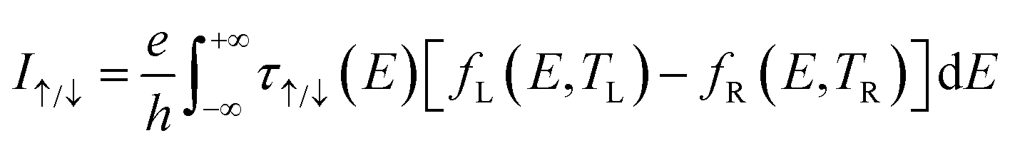
The two-dimensional B3C2P3 material (see Fig. S1, ESI†) is a planar honeycomb structure that looks like BP nanoribbons connected by C atoms. For graphene-like structures, zigzag direction cutting is more likely to introduce magnetism compared to armchair direction cutting. Therefore, we tailor the B3C2P3 monolayer along the zigzag direction, exposing the outermost edge atoms. Taking nanoribbons with widths of 4–6 atomic chain widths as examples, four bare zigzag B3C2P3 nanoribbons with different edge configurations can be obtained based on the combinations of the outermost atoms at the top and bottom edges, as shown in Fig. 1(a). Furthermore, we have designed eight H-passivation schemes for each edge configuration. According to different passivation schemes, the 1s orbitals of H atoms hybridize with the 2p orbitals of B and C atoms as well as the 3p orbitals of P atoms at the edges in different degrees, resulting in variations of the electronic states and total magnetic moments of the B3C2P3 nanoribbons, thereby modulating the B3C2P3 nanoribbons with different electronic and magnetic characteristics. Taking the zCB_CP edge configuration as an example, the xy-plane side views of the H-passivated structures are presented in Fig. 1(b), which are named nH-zCB_CP_mH, with n/m referring to the number of passivated H-atoms at the top/bottom edges.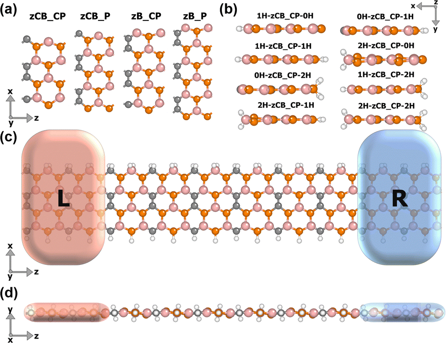 | ||
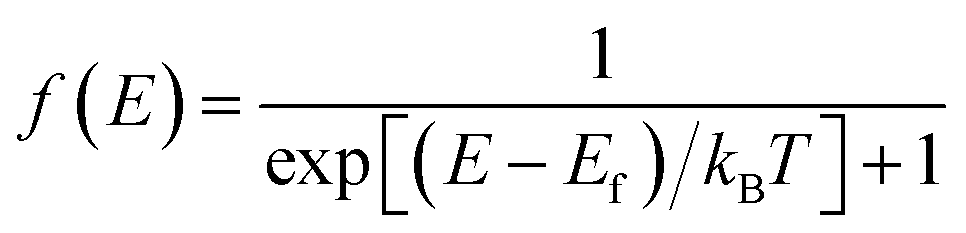
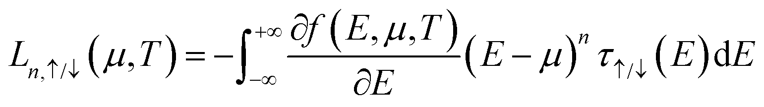
| Fig. 1 (a) Bare zigzag nanoribbons in four edge configurations. (b) Eight H-passivation schemes exemplified by zCB_CP. (c) and (d) Front and top views of a spin caloritronic device exemplified by 2H-zCB_CP-1H. All vacuum layers are not drawn here for display convenience. | ||
There are a total of 36 bare and hydrogen-passivated nanoribbons, and their total energies Etotal in NFM, FM, and AFM states are calculated in Table S1 (ESI†), where it can be found that the ground state of individual structures is the NM state, most of them are in the FM state, and the rest are in the AFM ground state, but the difference in energies between those in the AFM and the FM is not very large. Since the FM states can be stabilized by external magnetic fields in experiments and applications,34,35 all the work in this paper focuses only on the performance modulation in the FM state. For further calculations of the spin transport properties, spin caloritronic devices are designed, exemplified by the 2H-zCB_CP-1H configuration, as shown in Fig. 1(c) and (d), which consists of a central scattering region and two left and right semi-infinite electrodes with the same structure as it, without any other chemical interface between them in gapless connection.
These structures are fully geometrically relaxed by the DS-PAW (device studio-projector augmented wave)36 procedure based on a plane wave basis set, reaching the most structurally stable state with forces less than 0.01 eV Å−1 between each atom. The electronic and transport properties are calculated by the first principles calculation software Nanodcal37 package, based on the double-zeta polarized (DZP) atomic orbital basis set38 combining density-functional theory (DFT)39,40 with the non-equilibrium Green's function (NEGF).41,42 The exchange correlation energy is described by the Perdew–Burke–Ernzerhof (PBE) functional within the generalized gradient approximation (GGA).43 The norm-conserving pseudopotential is used to define the atomic cores.44 The mesh grids in k-space for calculating the transport properties are set to 1 × 1 × 100. The vacuum layers in the non-periodic direction of these structures are all larger than 15 Å excluding interactions between atomic layers.
Different temperatures are applied at the left and right terminals of the device without bias voltage, and the spin-resolved current driven by temperature difference is defined according to the Landauer–Büttiker formula:45
 | (1) |
 | (2) |
| τ↑/↓(E) = Tr[ΓL(E)GR↑/↓(E)ΓR(E)GA↑/↓] | (3) |
 | (4) |
 | (5) |
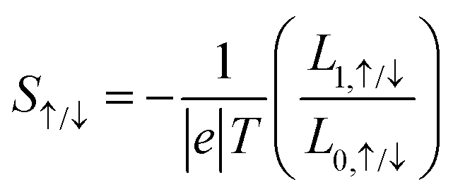
The charge Seebeck coefficient Sc and spin Seebeck coefficient Ss are expressed as 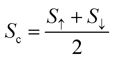 and Ss = S↑ − S↓, respectively. When different temperatures TL and TR are applied to the left and right ends of the device, the spin current formed by the spin voltage generated by the temperature gradient ΔT = TL − TR is denoted as Is = I↑ − I↓, and the charge current formed by the charge voltage is denoted as Ic = I↑ + I↓. Ss(Sc) indicates the ability to convert the temperature gradient into spin (charge) voltage.50
Results and discussion
Spintronic
The spin-resolved bands determine the spintronic properties. The first edge configuration, zCB_CP, was initially investigated by calculating the band structures of its bare and eight hydrogenated ones in the FM state, as shown in Fig. 2(a)–(i). Apparently, after self-consistent iteration with the FM state as the initial spin state, all other structures converge to the FM state, except for 2H-zCB_CP-2H in Fig. 2(i) which converges to the nonmagnetic state, showing nonmagnetism. Among them, bare zCB_CP exhibits magnetic metallic properties, and when its lower edge is saturated with single hydrogen (i.e., 0H-zCB_CP-1H), the C and P atoms at the lower edge shift from sp-hybridization to sp2-hybridization, but the band morphology near Ef does not undergo a significant change. Similarly, from 1H-zCB_CP-0H to 1H-zCB_CP-1H, the bottom edge turns from bare to monohydrogenated, and this change still does not have much effect on the spin-splitting band near Ef. Thus, for zCB_CP, saturation with monohydrogen on the bare CP bottom edge essentially does not change the electronic properties of the structure. This conclusion also holds true in the case of the dihydrogenated top edge, from 2H-zCB_CP-0H to 2H-zCB_CP-1H, both of which are semiconductors. However, by comparing these three pairs (from zCB_CP to 1H-zCB_CP-0H, from 0H-zCB_CP-1H to 1H-zCB_CP-1H, and from 0H-zCB_CP-2H to 1H-zCB_CP-2H, whose bare top edges are monohydrogenated), it can be seen that, regardless of whether the bottom edges are bare or mono- or di-hydrogenated, as long as the CB top edge is monohydrogenated, the structure is metallic. Furthermore, no matter whether the top or bottom edges are dihydrogenated, such as 2H-zCB_CP-0H and 0H-zCB_CP-2H, or both the top and bottom edges are dihydrogenated, i.e., 2H-zCB_CP-2H, as long as one of the edges is dihydrogenated, the configuration tends to be semiconducting. When this semiconducting dihydrogen saturation coexists with the metallic top-edge monohydrogenation (i.e., 1H-zCB_CP-2H), the bands traversing Ef are still present and are contained within the two semiconducting subbands, see Fig. 2(g), and thus 1H-zCB_CP-2H combines both top and bottom edge properties. For the second edge configuration zCB_P, its bare ribbon is also metallic (see Fig. 3(a)), and since its top edge is the same as that of zCB_CP, the dominant effect of hydrogen saturation at the top edge on the electronic properties remains unchanged, i.e., when the top edge is monohydrogenated, 1H-zCB_P-0H, 1H-zCB_P-1H, and 1H-zCB_P-2H show metallic properties, and when the top edge is dihydrogenated, the band gap at Ef opens and shows semiconducting properties, such as 2H-zCB_P-0H, 2H-zCB_P-1H, and 2H-zCB_P-2H. However, unlike zCB_CP, bare zCB_P has only P atoms on the bottom edge, and when these P atoms are passivated by a single H atom, a transition to semiconductors occurs (i.e., 0H-zCB_P-1H). This mechanism combined with the metallicity mechanism driven by the top monohydrogenated CB edge results in 1H-zCB_P-1H behaving as a metal.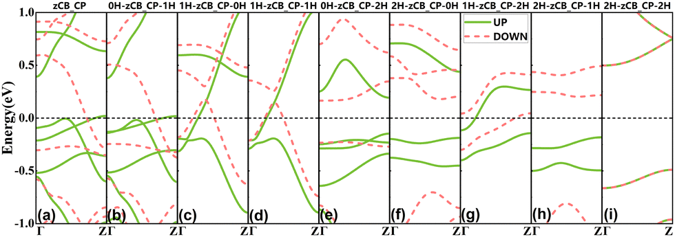 | ||
| Fig. 2 Band structures of zCB_CP for (a) bare and (b)–(i) eight H-passivation schemes in the initial FM state. The black dashed lines represent Fermi level Ef. | ||
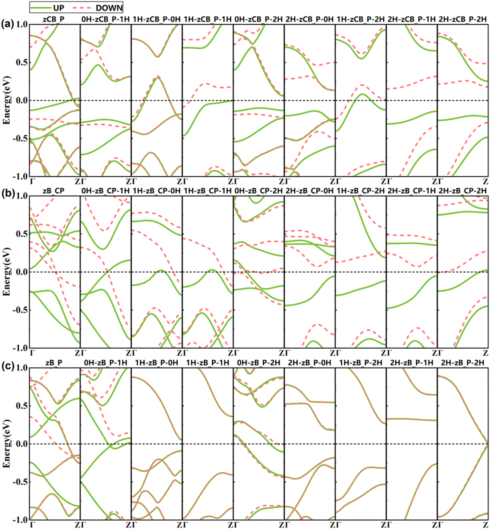 | ||
| Fig. 3 Band structures of (a) zCB_P, (b) zB_CP and (c) zB_P for bare and 8 edge H-passivation schemes in the initial FM state. The black dashed lines represent Fermi level Ef. | ||
For the other two edge configurations depicted in Fig. 3(b) and (c), zB_CP shows a transition from a semimetal to a magnetic metal to a bipolar magnetic semiconductor, whereas for zB_P, the system undergoes spin-splitting only when the top edge is exposed, while it is spin-degenerated in all other cases.
From the above discussion, it can be concluded that among these 36 structures, different edge hydrogen passivation schemes can effectively regulate the spintronic properties of the B3C2P3 nanoribbons, especially the 2H-1H passivation schemes, i.e., 2H-zCB_CP-1H, 2H-zCB_P-1H, and 2H-zB_CP-1H. These three structures show remarkable bipolar magnetic semiconductor properties with the potential for excellent spin-thermoelectric effects, and the thermodynamic stability of the structures was verified by ab initio molecular dynamics (AIMD) simulations (see Fig. S2, ESI†). Thus, the following discussion will focus on these three structures. Fig. 4(a) displays the spin density distribution of 2H-zCB_CP-1H, 2H-zCB_P-1H, and 2H-zB_CP-1H, which represent the spatial distribution of the charge difference between the spin up and down electrons.
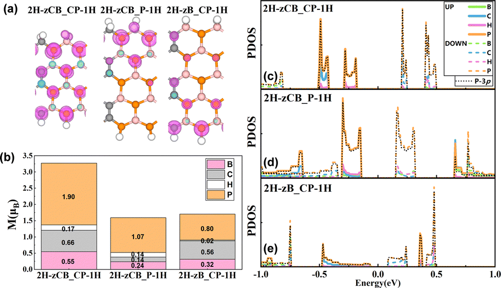 | ||
| Fig. 4 (a) Spin density distribution of 2H-zCB_CP-1H, 2H-zCB_P-1H, and 2H-zB_CP-1H with an isosurface value of 0.02 Å−3, with the purple and blue isosurfaces denoting higher spin-up and spin-down charge densities, respectively. (b) Atomic magnetic moment and (c)–(e) projected density of states of 2H-zCB_CP-1H, 2H-zCB_P-1H, and 2H-zB_CP-1H. | ||
Fig. 4(a) displays the spin density distribution of 2H-zCB_CP-1H, 2H-zCB_P-1H, and 2H-zB_CP-1H, which represents the spatial distribution of the charge difference between the spin up and down electrons.51 Apparently, the spin density of 2H-zCB_CP-1H features a bulk distribution, whereas those of 2H-zCB_P-1H and 2H-zB_CP-1H are localized at the top and bottom edges, respectively, and all of them exhibit significant magnetism. This is also supported by the calculated magnetic moments in Fig. 4(b), where 2H-zCB_CP-1H has the maximum moment of 3.27μB, and 2H-zCB_P-1H and 2H-zB_CP-1H have moments of 1.60μB and 1.70μB, respectively, and it is evident that P atoms in all the three structures account for the largest proportion of the total magnetic moment. Furthermore, in Fig. 4(c)–(e), the projected density of states (PDOS) near Ef are also mainly contributed by P atoms, especially their 3p orbitals. Thus, in all three B3C2P3 nanoribbons, the P atoms are the main source of magnetism and energy states around Ef.
Spin caloritronic transport properties
A particular transmission spectrum is necessary to produce excellent thermoelectric properties. As shown in Fig. 5, in agreement with the previous band structures and DOS, the transmissions of all three structures are suppressed at Ef, creating a transmission gap with spin-up and spin-down transmission channels located on either side of Ef, which is highly favorable for the emergence of SDSE. Specifically, 2H-zCB_CP-1H has the largest transmission gap at Ef and the narrowest transmission peaks on both sides, while 2H-zCB_P-1H has an intermediate transmission gap; noticeably, it has extremely symmetric spin-up and spin-down transmission peaks near Ef, which is more conducive to producing perfect SDSEs. 2H-zB_CP-1H, on the other hand, has the narrowest transmission gap and the widest transmission peaks with the highest transmission coefficient, which is favorable for generating large spin thermal currents. The spin-dependent transmission spectra of the 2H-zCB_CP-1H, 2H-zCB_P-1H, and 2H-zB_CP-1H show the commonality of bipolar magnetic semiconductors, as well as the presence of unique transport properties that differ from each other, which has intrigued us about their behavior in spin-thermoelectric transport.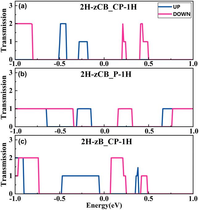 | ||
| Fig. 5 Spin-resolved transmission spectra of (a) 2H-zCB_CP-1H, (b) 2H-zCB_P-1H and (c) 2H-zB_CP-1H. | ||
The spin-dependent Seebeck coefficient Sσ, σ = ↑, ↓ characterizes the thermoelectric conversion ability, and eqn (4) and (5) shows that Sσ is related to the transmission coefficient and is also a function of the chemical potential μ and temperature. Fig. 6(a)–(c) plots the Sσversus chemical potential at different temperatures of 2H-zCB_CP-1H, 2H-zCB_P-1H and 2H-zB_CP-1H. As the temperature increases, the S↑ and S↓ peaks closest to μ = 0 eV shift to the right and left, respectively, but both peaks gradually decrease. In addition, since the transmission spectra of all three structures analyzed earlier show spin-bipolar magnetic semiconductivity, S↑ and S↓ near μ = 0 eV maintain the opposite sign, which leads to the corresponding Ss being much larger than Sc, as can be observed in Fig. 6(d)–(f). At 200 K, the Ss of 2H-zCB_CP-1H reaches a huge peak of 2 mV K−1 with a peak plateau at the interval of [−0.11, 0.12] eV, and the subsequent increase in temperature leads to smaller peaks and wider plateaus. At 100 K, the Ss peak of 2H-zCB_P-1H at μ = 0 eV is 1.5 mV K−1 at, and that of Ss of 2H-zB_CP-1H is the smallest, 730 μV K−1. After Ss reaches the peak, the peak Ss plateau broadens but then decreases as the temperature continues to increase, while the Sc at μ = 0 eV is always zero, and the Ss is much larger than the Sc. All three structures show obvious SDSE.
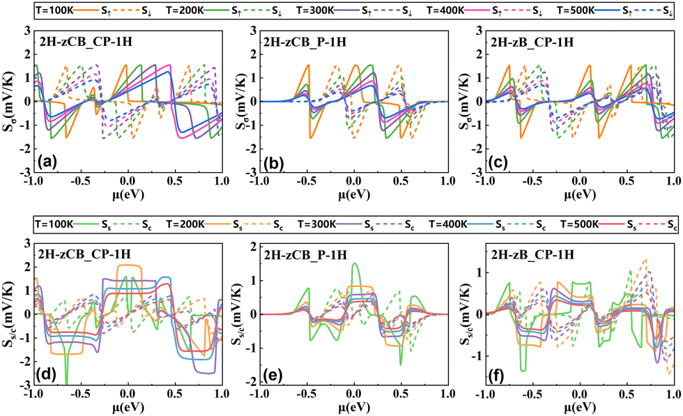 | ||
| Fig. 6 S σ of (a) 2H-zCB_CP-1H, (b) 2H-zCB_P-1H and (c) 2H-zB_CP-1H. Ss/c of (d) 2H-zCB_CP-1H, (e) 2H-zCB_P-1H and (f) 2H-zB_CP-1H. | ||
Applying different temperatures to the left and right electrodes of the device under zero bias, the spin-resolved currents Iσ, σ = ↑, ↓ can be generated driven by the temperature gradient ΔT. As shown in Fig. 7(a)–(c), the temperature of the left electrode is set higher than that of the right electrode, and when the left electrode reaches a certain temperature (i.e., the threshold temperature Tth), the current starts to be produced, and then increases with the increase of temperature. Apparently, the signs of I↑ and I↓ are opposite for these three structures, with negative I↑ and positive I↓, indicating that significant SDSE is induced in all three B3C2P3 nanoribbon devices. In contrast, 2H-zCB_CP-1H has the highest Tth of 250 K and the smallest current value of ∼10 nA, besides, at ΔT = 40 K, TL = 450 K and ΔT = 80 K, TL= 475 K, I↓ begins to decrease with increasing TL, resulting in a local negative differential thermoelectric resistance effect (NDTR). The Tth of 2H-zCB_P-1H is 225 K; in particular, I↓ and I↑ have the most comparable amplitude with the greatest potential to produce a perfect SDSE. 2H-zB_CP-1H has the smallest Tth of 100 K, indicating that this structure can be available for low-temperature driven devices, and furthermore, it can generate the largest Iσ of 200 nA, and produces a local NDTR at TL = 450 K, ΔT = 60, 80 K. Comparing the Tth of these three structures, 2H-zCB_CP-1H > 2H-zCB_P-1H > 2H-zB_CP-1H, which is consistent with the trend of the transmission gap, suggesting a positive correlation between Tth and the size of the transmission gap.
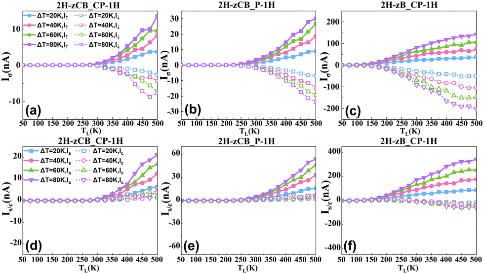 | ||
| Fig. 7 Spin-resolved current Iσ of (a) 2H-zCB_CP-1H, (b) 2H-zCB_P-1H and (c) 2H-zB_CP-1H. Spin/charge currents Is/c of (d) 2H-zCB_CP-1H, (e) 2H-zCB_P-1H and (f) 2H-zB_CP-1H. | ||
Additionally, the corresponding spin and charge currents of these three structures are calculated in Fig. 7(d)–(f). It is easy to find that after the threshold temperature is reached at the left electrode, Is of all three structures rise speedily with the increase of TL, whereas Ic only fluctuates slightly, and such discrepancy becomes more pronounced with the growth of ΔT, which results in the spin currents being much larger than the charge currents and all of them manifest the typical SDSE. Particularly noticeably, the 2H-zCB_P-1H structure exhibits near-perfect SDSE, due to its most spin-symmetric transmission spectrum. When Is of 2H-zCB_P-1H increases continuously with the left electrode and the temperature difference, the opposite is true for Ic, which is persistently suppressed extremely close to zero, enabling the generation of pure spin currents in 2H-zCB_P-1H. The excellent performance over a wide temperature range ensures that 2H-zCB_P-1H is suitable for a wide range of temperatures, making 2H-zCB_P-1H an ideal spin caloritronic device. On the other hand, 2H-zB_CP-1H generates the largest Is at the same temperature configuration compared to the other two structures, and attains a huge Is of 344.6 nA at TL = 500 K and ΔT = 80 K. Although the resulting Ic is non-negligible, Is is still much larger than Ic, and does not have to be driven by excessively high temperatures, hence the 2H-zB_CP-1H also performs a remarkable SDSE and is an excellent spin caloritronic device.
The formation mechanism of SDSE is analyzed by taking 2H-zCB_P-1H as an example. According to eqn (1), Iσ is obviously determined by the difference of the Fermi distributions together with the transmission spectrum. As can be seen from Fig. 8(a), above Ef, the Fermi Dirac distribution in the left high-temperature region is larger than that in the right low-temperature region, i.e., the electron concentration in the high-temperature region is higher than that in the low-temperature region, and that what exists above Ef is the spin-down transmission channel (see Fig. 5(c)), so that the electrons diffuse from the high-temperature region to the low-temperature region by means of the spin-down transmission channel, i.e., they flow from left to right, and form a right-to-left I↓. Similarly, below Ef, the concentration of holes on the left lead is higher than that on the right lead, so holes move from left to right through the spin-up transmission channel, forming a left-to-right I↑, and thus I↑ and I↓ are in opposite directions, resulting in SDSE. In order to further shed light on the current variations, the current spectrum Jσ(E) = τσ(E)[fL(E, TL) − fR(E, TR)], σ = ↑, ↓52 is plotted in Fig. 8(b) for different ΔT at TL = 500 K. Clearly, J↑ is always opposite in sign to J↓, and the values of Jσ increase gradually as the ΔT increases. One can also find that there is only one Jσ in the energy range [−0.3, 0.3] eV near Ef owing to the Fermi distribution difference, which implies that Iσ is determined by the transmission coefficients and Fermi distribution around Ef. When the spin up and spin down transmission coefficients on the left and right sides of Ef are exactly equal in a bipolar magnetic semiconductor, I↑ and I↓ can be generated in the opposite direction and with exactly equal magnitude, resulting in a large Is while a zero Ic, thereby yielding an optimal SDSE.
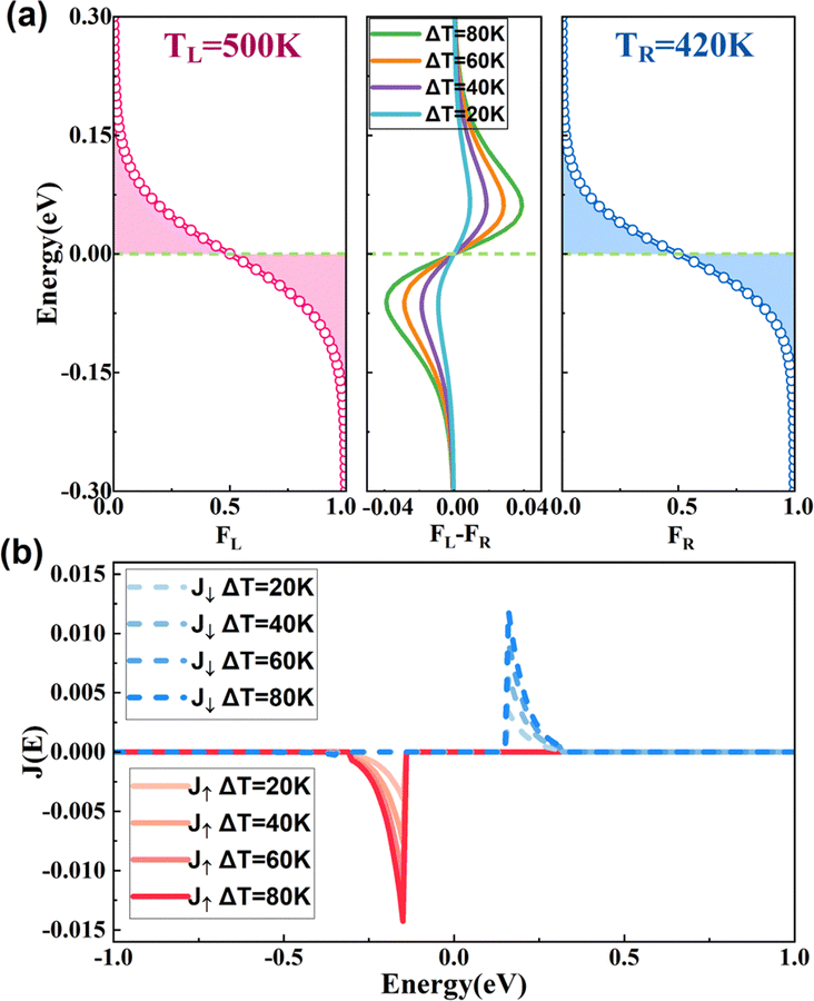 | ||
| Fig. 8 (a) Left is the Fermi Dirac distribution of TL = 500 K, right is the Fermi Dirac distribution of TR = 420 K, and the middle is the difference between the Fermi distributions of the left and right electrodes. (b) Current spectrum of 2H-zCB_P-1H. | ||
Conclusions
In this paper, based on the recently reported two-dimensional B3C2P3, four edge configurations of B3C2P3 nanoribbons are obtained by cutting it along the zigzag direction, including zCB_CP, zCB_P, zB_CP and zB_P. Various edge H-passivation schemes have been proposed to modulate their transport properties. Among them, the asymmetric passivation scheme 2H-1H has resulted in all three structures exhibiting bipolar magnetic semiconductor properties, except for 2H-zB_P-1H, which has spin-degenerated bands. The analytical results show that the magnetism in these three structures originates mainly from edge P-atoms. In addition, the Ss of these three nanoribbons at 0 eV is much larger than Sc, among which the 2H-zCB_CP-1H reaches a huge Ss of 2 mV K−1 at 200 K. Meanwhile, all three nanoribbons have I↑ in the opposite direction of I↓, so the Is generated are much larger than the Ic, and all exhibit excellent SDSE. Therefore, our 2H-1H asymmetric edge H-passivation scheme can effectively modulate the spin caloritronic transport performance of B3C2P3 nanoribbons, which enhances the application value of the novel material B3C2P3 and provides ideas for designing spin caloritronic devices.Author contributions
Jing-Jing He: conceptualization, methodology, writing – review & editing. Jia-Bei Dong: investigation, data curation, writing – original draft. Ling-Xiao Liu: methodology, data curation, visualization. Qin-Yue Cao: software, validation. Jun-Yi Gu: visualization, formal analysis. Ying Zhang: methodology, resources. Min Hua: visualization, formal analysis. Jia-Ren Yuan: software, supervision. Xiao-Hong Yan: supervision.Data availability
The data supporting this article have been included as part of the ESI.†Conflicts of interest
There are no conflicts to declare.Acknowledgements
This work was supported by the National Natural Science Foundation of China (Grant No. 62201268, 12264026), the National Key Research and Development Program of China (Grant No. 2022YFA1405200), the Natural Science Foundation of Jiangxi Province, China (Grant No. 20224BAB211013), the Innovation and Entrepreneurship Leading Talent Plan of Jiangxi Province (Grant No. Jxsq2023101068), and the China Scholarship Council (CSC Student ID 202408320264). We are grateful to HZWTECH for the support of computing facilities and technical communication.References
- Y. Ni, K. L. Yao, H. H. Fu, G. Y. Gao, S. C. Zhu and S. L. Wang, Sci. Rep., 2013, 3, 1380 CrossRef PubMed.
- H. Hao, H. Li, T. Jia, Y. Zhou and X. Zheng, Phys. Chem. Chem. Phys., 2024, 26, 12652–12660 RSC.
- S. Pei, R. Cao, Y.-H. Zhou, X. Zheng and C. Wang, New J. Phys., 2024, 26, 043014 CrossRef CAS.
- L. Kang, Y. Deng, X. Zheng, P. Jiang, Z. Feng, W. Wang and G. Zhao, Appl. Phys. Lett., 2024, 124, 132902 CrossRef CAS.
- L. Song, R. Ye, C. Su, C. Wei, D. Chen, X. Liu, X. Zheng and H. Hao, Phys. Rev. B, 2024, 109, 094105 CrossRef CAS.
- J. Xu, M. Li, Q. Wang, X. Zhang, J. Fei, Y. Shi, B. Zhang and M.-Q. Long, J. Phys. D: Appl. Phys., 2023, 56, 445301 CrossRef CAS.
- K. Uchida, S. Takahashi, K. Harii, J. Ieda, W. Koshibae, K. Ando, S. Maekawa and E. Saitoh, Nature, 2008, 455, 778–781 CrossRef.
- J. W. Li, B. Wang and J. M. Wang, Phys. E, 2019, 112, 109–114 CrossRef CAS.
- X. Deng, Z. Zhang, G. Tang, Z. Fan and C. Yang, Carbon, 2014, 66, 646–653 CrossRef CAS.
- M. G. Zeng, Y. P. Feng and G. C. Liang, Nano Lett., 2011, 11, 1369–1373 CrossRef CAS PubMed.
- Y. J. Dong, Y. Z. Wu, X. F. Wang, X. F. Yang and Y. S. Liu, J. Phys. Chem. C, 2019, 123, 29126–29132 CrossRef CAS.
- Q.-B. Liu, D.-D. Wu and H.-H. Fu, Phys. Chem. Chem. Phys., 2017, 19, 27132–27139 RSC.
- K. Zberecki, R. Swirkowicz, M. Wierzbicki and J. Barnaś, Phys. Chem. Chem. Phys., 2014, 16, 12900–12908 RSC.
- S. Kharwar, S. Singh and N. K. Jaiswal, Phys. B, 2021, 615, 413072 CrossRef CAS.
- P. Jiang, X. Tao, H. Hao, L. Song, X. Zheng and Z. Zeng, RSC Adv., 2017, 7, 28124–28129 RSC.
- H. H. Fu, D. D. Wu, Z. Q. Zhang and L. Gu, Sci. Rep., 2015, 5, 10547 CrossRef.
- Y. H. Zhou and X. H. Zheng, J. Phys.: Condens. Matter, 2019, 31, 315301 CrossRef CAS.
- K. Zberecki, R. Swirkowicz and J. Barnas, Phys. Rev. B: Condens. Matter Mater. Phys., 2014, 89, 165419 CrossRef.
- Y. Chang, A. Nie, S. Yuan, B. Wang, C. Mu, J. Xiang, B. Yang, L. Li, F. Wen and Z. Liu, Nanotechnology, 2018, 30, 035701 CrossRef.
- Y. Liu, Y. Yang, Y. Qu, Y.-Q. Li, M. Zhao and W. Li, Phys. Chem. Chem. Phys., 2020, 22, 23268–23275 RSC.
- X. Y. Tan, L. N. Zhang and L. L. Liu, Chem. Phys. Lett., 2020, 748, 137386 CrossRef CAS.
- K. Zberecki, R. Swirkowicz, M. Wierzbicki and J. Barnas, Phys. Chem. Chem. Phys., 2015, 17, 1925–1933 RSC.
- J. Guan, D. Liu, Z. Zhu and D. Tománek, Nano Lett., 2016, 16, 3247–3252 CrossRef CAS PubMed.
- A. A. Kistanov, S. A. Shcherbinin, S. V. Ustiuzhanina, M. Huttula, W. Cao, V. R. Nikitenko and O. V. Prezhdo, J. Phys. Chem. Lett., 2021, 12, 3436–3442 CrossRef CAS PubMed.
- W. C. Tan, Y. Cai, R. J. Ng, L. Huang, X. Feng, G. Zhang, Y. W. Zhang, C. A. Nijhuis, X. Liu and K. W. Ang, Adv. Mater., 2017, 29, 1700503 CrossRef PubMed.
- X. Huang, Y. Cai, X. Feng, W. C. Tan, D. M. N. Hasan, L. Chen, N. Chen, L. Wang, L. Huang, T. J. Duffin, C. A. Nijhuis, Y.-W. Zhang, C. Lee and K.-W. Ang, ACS Photonics, 2018, 5, 3116–3123 CrossRef CAS.
- A. López-Castillo, Int. J. Quantum Chem., 2012, 112, 3152–3157 CrossRef.
- J. Dong, H. Li and L. Li, NPG Asia Mater., 2013, 5, e56 CrossRef CAS.
- S. Huber, V. Medvedev, E. Gullikson, B. Padavala, J. H. Edgar, R. W. van de Kruijs, F. Bijkerk and D. Prendergast, Phys. Chem. Chem. Phys., 2017, 19, 8174–8187 RSC.
- W. L. Wang, X. D. Bai, K. H. Liu, Z. Xu, D. Golberg, Y. Bando and E. G. Wang, J. Am. Chem. Soc., 2006, 128, 6530–6531 CrossRef CAS.
- J. Wu and Y.-X. Yu, J. Phys. Chem. C, 2022, 126, 12460–12471 CrossRef CAS.
- H. Al-Jayyousi, M. K. Eswaran, A. Ray, M. Sajjad, J. A. Larsson and N. Singh, ACS Omega, 2022, 7, 38543–38549 CrossRef CAS.
- X. Fu, J. Lin, X. Cheng, W. Liao, J. Guo, X. Li and L. Li, Mater. Today Commun., 2023, 35, 106175 CrossRef CAS.
- P. Jiang, X. X. Tao, H. Hao, L. L. Song, X. H. Zheng, L. Zhang and Z. Zeng, 2D Mater., 2017, 4, 035001 CrossRef.
- L. Lei, Y.-H. Zhou, X. Zheng, W. Wan and W. Wang, Phys. Chem. Chem. Phys., 2024, 26, 3253–3262 RSC.
- P. E. Blöchl, Phys. Rev. B: Condens. Matter Mater. Phys., 1994, 50, 17953 CrossRef.
- J. Taylor, H. Guo and J. Wang, Phys. Rev. B: Condens. Matter Mater. Phys., 2001, 63, 245407 CrossRef.
- C. He, Y.-L. Li, Z.-G. Sun, J.-F. Wang and M.-Y. Chen, Phys. E, 2022, 143, 115333 CrossRef CAS.
- X. Zheng, Z. Zheng, S. Yang, C.-S. Liu, L. Zhang and H. Hao, Phys. Rev. B, 2024, 110, 115439 CrossRef.
- X. Zheng, S. Yang, Z. Zheng, C.-S. Liu, W. Wang and L. Zhang, Appl. Phys. Lett., 2024, 125, 223503 CrossRef CAS.
- L. Song, C. Wei, D. Chen, R. Ye, C. Su, Y. Yang, X. Zheng and H. Hao, Comput. Mater. Sci., 2024, 245, 113290 CrossRef CAS.
- Z. Han, X. Zheng, C.-S. Liu, L. Zhang, W. Wang and Z. Zeng, IEEE Trans. Electron Dev., 2024, 71, 7169–7176 Search PubMed.
- H. Yu, Y. Li, D. Wei, G. Guo, Z. Feng, J. Ye, Q. Luo, Y. Ma, Y. Tang and X. Dai, Micro Nanostruct., 2022, 165, 207188 CrossRef CAS.
- J. Yang, X. Yu, Z. Yu and L. Zhang, Europhys. Lett., 2021, 135, 46001 CrossRef CAS.
- U. Sivan and Y. Imry, Phys. Rev. B: Condens. Matter Mater. Phys., 1986, 33, 551–558 CrossRef CAS PubMed.
- J. Aarons, M. Sarwar, D. Thompsett and C.-K. Skylaris, J. Chem. Phys., 2016, 145, 220901 CrossRef.
- I. Zutic, J. Fabian and S. Das Sarma, Rev. Mod. Phys., 2004, 76, 323–410 CrossRef CAS.
- G. Q. Ding, M. Wei, G. Surucu, Z. Y. Liang and X. T. Wang, Appl. Surf. Sci., 2019, 491, 750–756 CrossRef CAS.
- Y. Jiang, Y. D. Guo, L. Y. Lin and X. H. Yan, Nanoscale, 2022, 14, 10033–10040 RSC.
- P. Jiang, X. Tao, L. Kang, H. Hao, L. Song, J. Lan, X. Zheng, L. Zhang and Z. Zeng, J. Phys. D: Appl. Phys., 2018, 52, 015303 CrossRef.
- H. Wang, M. Wang, C. Qian, X. Hong, D. Zhang, Y. Liu and X. Yang, Phys. Lett. A, 2017, 381, 1738–1744 CrossRef CAS.
- X.-J. Gao, P. Zhao and G. Chen, Chem. Phys. Lett., 2018, 699, 250–254 CrossRef CAS.
Footnote |
| † Electronic supplementary information (ESI) available. See DOI: https://doi.org/10.1039/d4cp03033h |
| This journal is © the Owner Societies 2025 |