
Exploring the potential of malononitrile functionalized donor–acceptor systems for non-volatile memory device applications†
Ramachandran
Gokul
a,
Ramesh
Gayathri
a,
Predhanekar Mohamed
Imran
b,
Nattamai S. P.
Bhuvanesh
c and
Samuthira
Nagarajan
 *a
*a
aDepartment of Chemistry, Organic Electronics Division, Central University of Tamil Nadu, Thiruvarur 610 005, India. E-mail: snagarajan@cutn.ac.in
bDepartment of Chemistry, Islamiah College, Vaniyambadi, 635 752, India
cDepartment of Chemistry, Texas A&M University, College Station, TX 77842, USA
First published on 27th November 2024
Abstract
A novel series of D-bridge-A type organic small molecules has been designed, synthesized, and evaluated for non-volatile resistive switching write-once read-many (WORM) memory application. This study explores structure–property relationships by coupling electron-deficient malononitrile units with donors such as dibenzofuran, dibenzothiophene, and triphenylamine. Photophysical investigations revealed significant intramolecular charge transfer interaction, while electrochemical analyses demonstrated optimal band gaps ranging from 2.20 to 3.10 eV. All synthesized compounds exhibited robust, non-volatile, resistive switching memory capabilities, with ON/OFF ratios spanning 102 to 103. The lowest recorded threshold voltage was −1.25 V, and devices demonstrated substantial stability with retention times of 103 s. Notably, triphenylamine-based compounds displayed superior memory performance compared to their counterparts. The solubility of the compounds in common organic solvents suggests that they are viable for cheap fabrication techniques. Density functional theory calculations were used to visualize the key molecular orbitals and support the proposed mechanisms for resistive switching. The strategic implementation of equipotential donors and acceptors is highly desirable. This well-rounded approach guarantees optimal performance and fosters broader applicability of these devices.
Introduction
In the digital age, the constant quest for more data storage capacity has led to a fundamental shift in the design of electronic devices. Even while germanium and silicon have unquestionably advanced technology for many years, it is becoming increasingly clear that these materials cannot fully satisfy the world's unquenchable need for high-density data storage. These traditional materials are reaching their physical scaling limits, hindering the development of smaller, faster, and more energy-efficient memory devices. In response, the scientific community is exploring the potential of organic materials to revolutionize memory devices.1 These carbon-based compounds offer unique properties such as flexibility, low cost, and the potential for large-scale, solution-based processing, presenting a promising avenue for overcoming the challenges posed by conventional materials.2 These attributes facilitate the potential for high-density data storage, rapid information processing, and energy-efficient operation, which are the key requirements for future computing paradigms.3 These materials have an advantage over inorganic alternatives as they can be manufactured at lower temperatures and on flexible surfaces, allowing for innovative device designs. However, the practical use of some organic materials has been limited by their tendency to degrade, particularly through oxidation and light exposure. To overcome this challenge, scientists are creating new materials by introducing different groups into organic conjugated structures to improve stability and functionality. Key strategies include the modulation of molecular architecture through targeted functional group engineering and manipulating molecular packing arrangements. A particularly efficacious approach involves incorporating electron donor–acceptor (D–A) moieties into the molecular design framework. These D–A systems facilitate charge transfer interactions, crucial in forming and disrupting conductive filaments—the fundamental mechanism underlying resistive switching phenomena. By tailoring the D–A system's electronic properties, researchers can exert control over critical device parameters, including resistance states, switching kinetics, and operational endurance.4 This molecular-level engineering approach enables fine-tuning memory device performance characteristics to meet specific application requirements.5 The resultant devices exhibit a broad spectrum of memory characteristics, ranging from volatile to non-volatile behaviour. These properties are governed by various factors, including the stability of charge transfer complexes, the presence and nature of charge trapping sites, and the specifics of the device fabrication methodology.6In this work, we have focussed on malononitrile as the core acceptor, paired with diverse donor moieties. Malononitrile, a tiny, planar molecule characterized by twin cyano groups surrounding a reactive methylene bridge, has a strong electron-drawing ability and a high electron affinity. These properties, together with its thermal stability and solution processability, make malononitrile an adaptable component in the synthesis of electron-transporting materials and donor–acceptor systems. Its ability to facilitate efficient charge transfer, promote molecular packing through π–π stacking, and allow facile functionalization has led to the widespread adoption in the development of organic light-emitting diodes (OLEDs),7 organic field-effect transistors (OFETs),8 and organic photovoltaics (OPVs).9 The insertion of malononitrile into larger molecular frameworks not only improves charge carrier mobility and electron injection but also helps to fine-tune electrical and optical characteristics, which are critical for improving the performance of organic electronic devices. In recent years, malononitrile has been used for memory device applications. Xiang et al.10 synthesized malononitrile functionalized phenothiazine molecule to fabricate RRAM device. The fabricated device shows binary WORM memory behavior with an ON/OFF current ratio of 102 at the threshold voltage of −1.85 V. Qi-Jian et al.11 designed an A–D–A-type molecule with a malononitrile group as a strong acceptor in the central part of the molecule and carbazole as a donor in the terminals connected by π-bridges. Furthermore, the device demonstrates exceptional ternary WORM memory performance with an ON/OFF current ratio of 1![[thin space (1/6-em)]](https://www.rsc.org/images/entities/char_2009.gif) :102.1:104.3 at threshold voltages of −1.33 V and −2.75 V. These superior memory characteristics are attributed to a combination of factors in the molecule, including high electron transport and low LUMO energy level.
:102.1:104.3 at threshold voltages of −1.33 V and −2.75 V. These superior memory characteristics are attributed to a combination of factors in the molecule, including high electron transport and low LUMO energy level.
The previously reported works include complex multistep synthetic methodologies that are not economically and industrially viable. This study highlights the simple two-step synthesis of organic compounds based on malononitrile for high-performance resistive switching memory devices. The interplay between molecular design, thin-film morphology, and charge transport properties offers exciting opportunities for further optimization and development of next-generation organic memory technologies.
Results and discussion
Design and synthesis
D-bridge-A architectured compounds have been designed and synthesized, and malononitrile serves as the electron acceptor. This acceptor is linked to different electron donors, including dibenzofuran, dibenzothiophene, and triphenylamine. The donors and acceptors are connected using various bridging units, specifically benzene, thiophene, and pyridine. The synthesized compounds 9a–f were used to investigate the structure–property relationship and the influence of various donors on memory performance. The molecular structure of the compounds and the detailed synthetic route are provided in Fig. 1 and Schemes S1 and S2 (ESI†). The acceptor part is fixed with malononitrile, a tiny, planar molecule characterized by two cyano groups surrounding a reactive methylene bridge, and has a strong electron-withdrawing ability. Further, Active methylene groups are highly reactive sites for chemical modification due to their propensity to undergo various condensation reactions. This characteristic makes them invaluable for constructing complex molecules. Various donor moieties, including dibenzofuran, dibenzothiophene, and triphenylamine (TPA), have been incorporated to counterbalance the electron-withdrawing nature. TPA's bulky, propeller-like structure enhances the stabilization of the charge-separated state. Dibenzofuran and dibenzothiophene exhibit superior chemical and thermal stability, which are crucial for the long-term performance and lifespan of the resulting devices.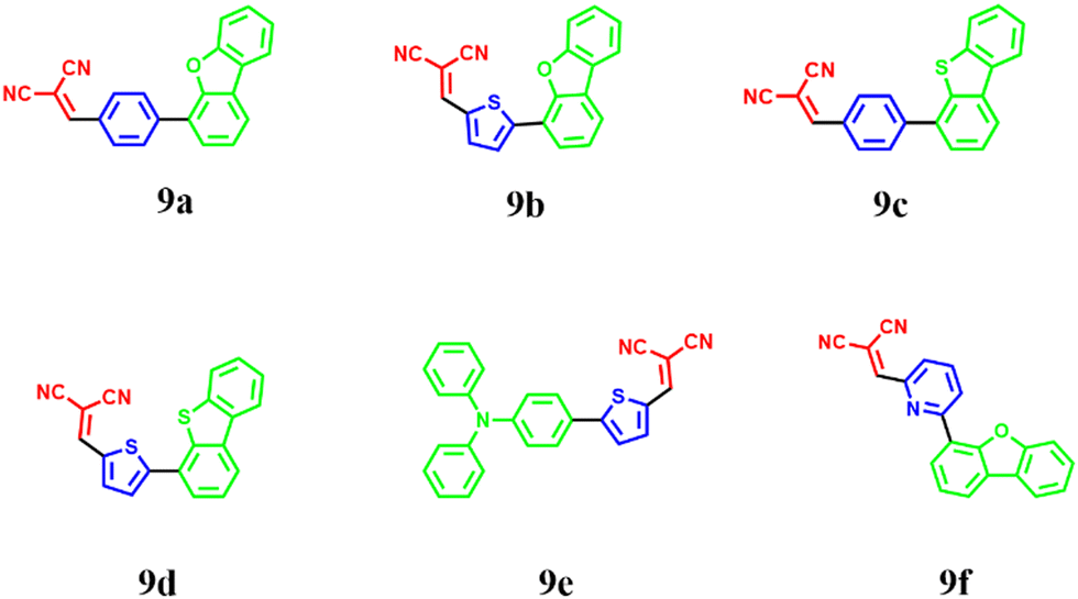 | ||
| Fig. 1 Molecular structure of the synthesized compounds 9a–f. | ||
In this work, Knoevenagel condensation reactions using DABCO as a catalyst made a series of equipotent donor–acceptor systems. Donor and acceptor parts are linked through phenyl, thienyl, and pyridine bridges, further enhancing the molecule's pi-conjugation, rigidity, and stability. The synthesized compounds’ structure was validated using 1H NMR, 13C NMR, IR, and HRMS spectroscopic techniques (Fig. S1–S26, ESI†).
Thermogravimetric analysis
The thermal stability of the compounds was assessed through thermogravimetric analysis (TGA) under nitrogen conditions. The results, shown in Fig. 2, indicate that all the compounds exhibited decomposition temperatures above 280 °C. Triphenylamine substituted compound 9e displayed the highest decomposition temperature at 350 °C. These findings confirm the exceptional thermal stability of all compounds, ensuring their resistance to degradation during device manufacturing processes or operations. This inherent stability is crucial for the long-term reliability and performance of memory devices.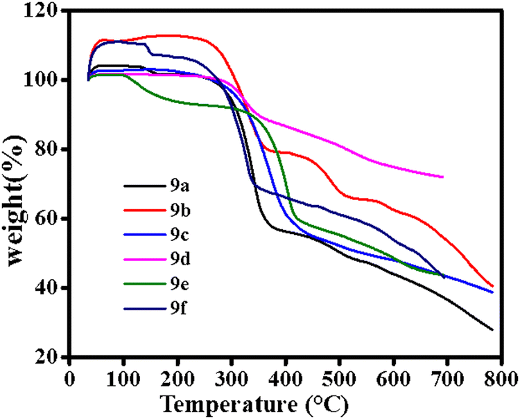 | ||
| Fig. 2 TGA curve for compounds 9a–f. | ||
Photophysical studies
Assessing the photophysical characteristics of the synthesized compounds is imperative to confirm the donor–acceptor interaction strategy and to examine their charge transfer capabilities. Photophysical properties of the synthesized compounds 9a–f were studied using absorption and emission spectra in tetrahydrofuran at 10−5 M and 10−7 M concentrations, respectively. In consonance with the data presented in Table 1, all the investigated compounds exhibited a maximal absorption wavelength (λmax) within the ultraviolet (UV) region, ranging from 356 to 485 nm (Fig. 3a). This demonstrates the intramolecular charge transfer (ICT) contributed to the inherent donor–acceptor character of the synthesized compounds. The addition of different substituent and their relative position accelerates the charge transfer to the electron-accepting dicyanide group. Compound 9e shows a broad charge transfer band around 485 nm, red-shifted from the other compounds due to the extended π-conjugation of triphenylamine moiety.12 Compounds 9a–f shows unique peaks in the absorption band around 291–309 nm due to π–π* electronic transitions.13 The characteristic shoulder band at 296 and 351 nm corresponds to the n–π* transition in compounds 9d and 9e, respectively. Compound 9e exhibits a bathochromic shift in its n–π* absorption band compared to 9d, accounting for the improved electron-donating ability of triphenylamine in compound 9e. However, the n–π* transition is not clearly visible for other compounds and may be merged with the charge transfer band.14,15 Thiophene's non-bonding electrons expanded the UV-vis absorption edge to a longer wavelength in compounds 9b, 9d, and 9e compared to other compounds. All these observations indicate that the molecules have a superior electron-donating and accepting group and have been appropriately conjugated. Steady-state fluorescence spectra were recorded for compounds 9a–f to investigate the photophysical properties of their excited states and their interactions with the solvents. The excitation spectra were obtained by monitoring the emission intensity as a function of excitation wavelength (Fig. 3b). All the compounds show similar emission spectra with a wavelength ranging from 395–626 nm. The Stokes shift was observed in the order 9e > 9c > 9f > 9a > 9b > 9d. The fluctuation in Stokes’ shift of the compounds is caused by the varied geometry of compounds in the ground and excited states,. Compound 9d shows a lower Stokes shift, which is attributed to the more rigid nature of the compound, leading to the exited state geometry resembling the ground state geometry more.| Compounds 9 | λ max (abs) (nm) | λ em (nm) | Stokes shift (nm) | Absorption coefficient (103 mol−1 cm−1) |
|---|---|---|---|---|
| a | 356 | 433 | 77 | 34 |
| b | 408 | 463 | 55 | 26 |
| c | 369 | 505 | 136 | 5.9 |
| d | 410 | 395 | 15 | 30 |
| e | 485 | 626 | 141 | 33 |
| f | 353 | 466 | 113 | 6.6 |
 | ||
| Fig. 3 (a) UV-Visible absorption (10−5 M) and (b) emission spectra (10−7 M) of compounds 9a–f in THF. | ||
Electrochemical properties
Recognizing the electronic behaviour of a material and its function in electrochemical processes requires an understanding of the concepts of HOMO (highest occupied molecular orbital) and LUMO. The electronic structure and redox activity of the compounds are strongly influenced by the HOMO–LUMO bandgap. The electrochemical characteristics of the synthesized compounds 9a–f were examined using cyclic voltammetry. Fig. 4 depicts the cyclic voltammogram for the compounds 9a–f, and the data are summarized in Table 2. The apparatus setup includes three electrodes: a platinum wire counter electrode, a glassy carbon working electrode, and a standard calomel reference electrode. Initially, the setup was calibrated using ferrocene. Later, compounds 9a–f underwent cyclic voltammetric investigation in N,N-dimethylformamide solvent with 0.1 M Bu4NPF6 as the supporting electrolyte. Compounds 9a–f exhibit the first oxidation peak around 1.04–1.50 V. Upon scanning in the opposite direction in compound 9e, a peak in the same region indicates that the oxidation is reversible. All the compounds display an irreversible peak on the cathodic side, characteristic of the corresponding cyanide reduction at around 0.82 eV. HOMO values of the compounds were computed by using the oxidation potential value of ferrocene against a standard calomel electrode, employing the formula EHOMO = (4.80 − EFerrocene + Eox). The HOMO levels of compounds 9a–f ranges between −5.33 to −5.42 V. The low-lying HOMO levels are attributed to the high oxidation stability of compounds 9a–f.16 Due to two electron-withdrawing cyano groups attached to the backbone, LUMO energy levels are significantly lowered.17 The LUMO level ranges between −2.30 and −3.20 V. The band gap of compounds 9a–f ranges in the order 9e < 9d < 9b < 9e < 9a < 9f and spans between 2.20 and 3.10 eV, which is an appreciable range for the semiconducting property of the compounds. Compound 9e is particularly interesting since it has a noticeably smaller band gap (2.20 eV) than other compounds. This can be explained by the expanded π-conjugation and electron-donating ability of the triphenylamine unit.18 These findings suggest effective charge transfer within the compounds, which may improve their resistive switching performance. | ||
| Fig. 4 SEM images of the thin – films of compounds 9a–f. | ||
| 9 | Experimental | Computational | |||||
|---|---|---|---|---|---|---|---|
| E ox (V) | E HOMO (eV) | E LUMO (eV) | E g (eV) | E HOMO (eV) | E LUMO (eV) | E g (eV) | |
| a | 1.50 | −5.38 | −2.30 | 3.04 | −6.33 | −2.83 | 3.49 |
| b | 1.08 | −5.36 | −2.65 | 2.71 | −6.05 | −2.89 | 3.16 |
| c | 1.09 | −5.35 | −2.36 | 2.98 | −6.09 | −2.90 | 3.18 |
| d | 1.06 | −5.42 | −2.71 | 2.63 | −6.04 | −2.92 | 3.12 |
| e | 1.11 | −5.40 | −3.20 | 2.20 | −5.33 | −2.75 | 2.58 |
| f | 1.04 | −5.33 | −2.23 | 3.10 | −6.32 | −3.00 | 3.31 |
Morphology of thin-films
Scanning electron microscopy (SEM) was utilized to investigate the surface morphology and uniformity of the active layer. The thin film's microstructure is vital in influencing the device's performance. High-resolution morphological characterization of the thin films was achieved using scanning electron microscopy (SEM). The films exhibited remarkable self-assembly properties. SEM images, captured at various magnifications, revealed exceptional surface coverage, indicative of highly homogeneous thin-film formation for all the compounds. Compounds 9a and 9f have a dense needle-like network, whereas compound 9b has a petal-like morphology. Compound 9c has a spindle fibrous network, and 9d has a coral-like network with excellent coverage over the entire surface. Rod-like arrangement was exhibited by compound 9e. These results reveal the creation of a robust and fully covered active layer, which leads to maximizing device performance by excellent charge transfer across the active layer. To gain further insight into the characteristics of the thin film, a cross-sectional image was captured using scanning electron microscopy (SEM) for the representative compound 9a (as illustrated in Fig. 5). This imaging technique provided valuable information about the film's thickness and its degree of uniformity across the substrate. | ||
| Fig. 5 SEM cross-section of thin-film of compound 9a. | ||
Atomic force microscopy (AFM) analysis of a representative compound, 9a, revealed a homogenous thin film with a remarkably smooth surface topography. The root mean square (RMS) roughness value of 12 nm (Fig. S29, ESI†) indicates a minimal deviation from the mean plane, suggesting an exceptionally flat film. This uniformity is expected to facilitate intimate contact with the electrode interfaces, thereby minimizing the formation of interfacial defects and reducing the potential for Ag nanoparticle diffusion into the film. The low roughness value is also anticipated to contribute to efficient charge. Studies using thin-film XRD were carried out to gain deeper insights into the thin-film properties of compounds. The d-spacing, which represents the distance between crystal planes, was then computed using Bragg's Law (nλ = 2dsinθ), where λ indicates the wavelength of X-rays. (Fig. S28, ESI†) represents the thin film XRD of the compounds 9a–f. High crystallinity is evident from all compounds’ sharp and intense peaks. Compounds 9a–f exhibit a pronounced peak at 2θ = 49.6° or 44.64°, corresponding to an interplanar distance of 1.85 or 2.03 Å. This sharp peak signifies exceptional molecular ordering, leading to high crystallinity in these compounds.19 All the compounds have a peak at 2θ of 72.7° with a d-spacing value of 1.29 Å. The lower d-spacing value of compounds signifies the molecules' strong intramolecular attraction and perfect self-assembly.20 Compounds 9b and 9c have a peak at 11.2° with a d-spacing value of 8.02 Å. The higher d-spacing value depicts the long-range ordered arrangement of the molecules on the surface of a coated glass plate. In addition, many less intense peaks were observed at various angles. In compound 9c, peaks at an angle of 22.9, 50.4 degrees, giving a d-spacing of 3.87,1.80 angstroms corresponds to the π–π stacking.21 Compound 9f shows two very sharp peaks at 2θ of 11.02° and 12.8° with a d-spacing of 7.3 Å and 6.93 Å. This sharp peak is due to increased hole mobility.22 In addition, the minor peaks at 2θ of 17.2, 17.7, and 25.7 degrees with d-spacing values of 6.72, 5.03, 3.46 angstroms may be due to the possible edge-by-edge molecular arrangement.23 Interestingly, the d-spacing value of 8.02 Å of the weak intense peak at 11.01 is almost double the d-spacing value of 4.03 at 2θ of 22.08 Å of the high intense peak. This ascribes the second-order diffraction phenomena in compounds 9b and 9c.24 The small d-spacing values imply tighter molecular packing, resulting in a high degree of self-assembly inside the compounds’ thin layer. Post-annealing of thin films is also beneficial for enhancing crystallinity and minimizing intermolecular spacing, reducing the frequency of film defects. The sharp and intense peaks imply that the thin film is highly crystalline and organized, which could lead to its application in memory devices.
The single crystals of compounds 9b and 9f were acquired by the gradual evaporation of chloroform solution, which was then analyzed through the single crystal XRD technique. Compound 9b exhibited a monoclinic crystal structure with a P21/n space group, while compound 9f had a monoclinic system with P21/c space group. The crystal packing of 9b and 9f revealed a lamellar-like packing pattern. The interactive distances between two crystals were measured along the π-stacking position and were found to be 3.1–5.9 Å for compound 9b and 3.1–4.0 Å for compound 9f. The crystal structure, it's packing, and its interactive distances are shown in Fig. 6. These packing patterns agree with the theoretically analyzed molecular packing and hoping distances (Fig. S33, ESI†). Also, these intermolecular distances ensure effective π-interactions with the possibility of charge transfer within the system.25
 | ||
| Fig. 6 (a) Single-crystal structure and (b) packing pattern of the compounds 9b and 9f with their interactive distances (Å). | ||
Memory characteristics
The synthesized malononitrile-based compounds were evaluated for their potential application in memory devices. ITO/9a–f/Ag layered devices were employed to analyze the memory characteristics. The I–V characteristics of the devices are illustrated in Fig. 7. During the initial sweep from 0 V to −7 V, the device began in the OFF or high resistance state (HRS) with a current of approximately 10−6 A. As the negative bias increased, a gradual rise in current was observed. | ||
| Fig. 7 Current–voltage (I–V) curves of fabricated device ITO/9a–9f/Ag. | ||
However, a significant current jump occurred at a particular voltage referred to as threshold voltage, which ranges from 1.25–1.85 V. This abrupt change signifies the transition from the HRS to the low resistance state (LRS). This transition corresponds to the writing process in memory devices.26 Notably, during subsequent voltage sweeps (both negative and positive), the device remained in the ON state. This inability to return to the OFF state and a retention time exceeding 24 hours confirms that device 9a–f follows a binary WORM memory behaviour.27
The ratio of current between the LRS and HRS, quantified by the ON/OFF ratio, is a critical parameter in resistive memory devices. Compounds 9a–e exhibit a significantly higher ON/OFF ratio of 103 than compound 9f (102). Interestingly, compound 9f also displays a higher threshold voltage of 1.85 V for resistive switching. This disparity can be attributed to the interplay between the electron-withdrawing nature of the pyridine bridge and the acceptor core malononitrile in 9f. While these moieties promote resistive switching, they might not be adequately balanced by the electron-donating character of the dibenzofuran unit in compound 9f. This imbalance could potentially hinder the complete transition to the LRS, resulting in a lower ON/OFF ratio for compound 9f. The lower threshold voltage was observed in compound 9e. This is because of the strong electron-donating property of the triphenylamine group, which properly balances the malononitrile core acceptor through the thiophene bridge.28 The observed trend in threshold voltage values (9e < 9d < 9b < 9a < 9f) aligns remarkably well with the band gap values obtained from the electrochemical studies. This correlation signifies that compounds with a lower band gap exhibit a lower threshold voltage for resistive switching and vice versa. This substantial agreement between the electrical and structural properties underscores the credibility and reproducibility of the fabricated devices’ performance, endurance and retention characteristics were evaluated using a constant voltage stress of 0.5 V for devices ITO/9a–f/Ag. Notably, these binary devices’ high (ON) and low (OFF) conductance states exhibited negligible variations throughout the testing process. The current-versus-time retention test spanned 1000 seconds, while the cycle-versus-current endurance test encompassed over 100 write per erase cycles. This remarkable stability across diverse operational states underscores the devices’ strong potential as reliable memory solutions. Fig. 8 visually depicts all devices’ endurance and retention performance of compounds 9a–f. Table 3 summarizes the memory device parameters for compounds 9a–f.
 | ||
| Fig. 8 (a) Retention time and (b) endurance cycle of devices ITO/9a/Ag. | ||
Different conduction models are analyzed to get deeper insights into the device's resistive switching phenomena. There are different conduction phenomena like Ohmic conduction, Schottky emission, hopping conduction, trap-controlled space-charge-limited conduction (SCLC), Poole–Frenkel (PF) conduction, through which conduction can be achieved over a material for a better resistive switching (RS) behaviour. In the low-voltage region, all compounds show ohmic conduction, as indicated by a unit slope (≈1) in the I–V curve. This represents a straight-line relationship between current and voltage, indicating unrestricted carrier flow with zero resistance. Compounds 9b, 9d, and 9f at higher voltages transform into a trap-filled space-charge-limited conduction (SCLC) process. This is shown by a steeper slope that exceeds 2, consistent with Child's Law, which states that current dependency scales with the square of the applied voltage (I proportional to V2).29 This implies the presence of traps restricting mobile carriers, which become loaded at higher voltages, resulting in a more noticeable current increase. Compounds 9a and 9d diverge from the trend, exhibiting a slope indicative of Poole–Frenkel (PF) conduction.30 This voltage leads to lower performance for this device. These findings emphasize the need to analyse slope values in I–V characteristics to determine the primary conduction mechanism in the RS device. The observed variations point to a possible influence of material qualities and specific substituents on the underlying transport processes (Fig. 9).
 | ||
| Fig. 9 Linear fitting plots of devices (ITO/9a–f/Ag). | ||
Computational studies
A series of computational simulations like molecular mechanics and semi-empirical methods were used to arrive at a plausible structure, which is an important aspect for packing and predicting the electronic properties of the system. These approximate geometrical parameters were then used to compute the optimized structure at the DFT's B3LYP level of theory (Fig. 11) and TD-SCF for spectral estimation theoretically using Gaussian (Table S2, ESI†). The optimized geometry was then used as input geometry for density of states (DOS) calculations using VASP (MedeA) software (Fig. S33, ESI†). However, the structures were evaluated involving solvent correction parameters such as GGA-PBE. The Fermi energy and band gaps were also evaluated. The crystallographic values obtained from VASP were then used to assign the crystal parameters and set up the packing pattern inside the discover studio module (Fig. S34, ESI†). The packing patterns were modelled with various group symmetry elements to arrive at a suitable packing pattern describing the non-covalent interaction.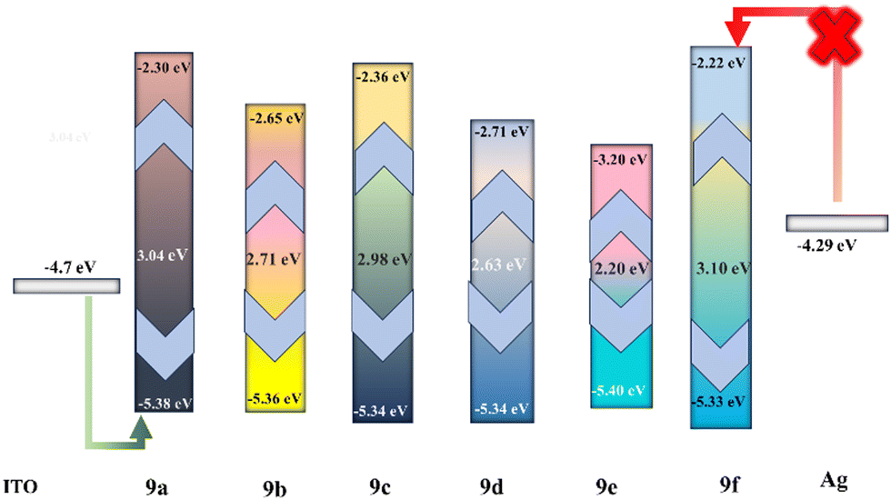 | ||
| Fig. 10 Energy level diagram of compounds 9a–f with the work function of electrodes. | ||
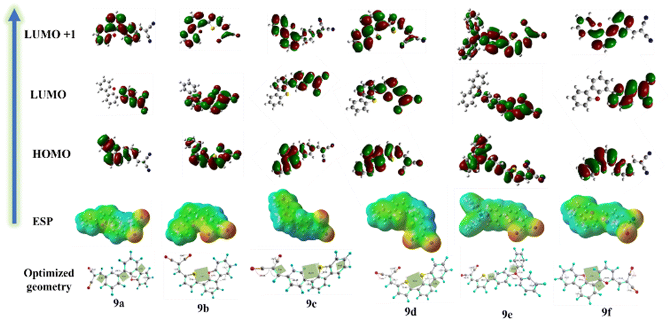 | ||
| Fig. 11 Molecular optimized geometry, ESP map and HOMO, and LUMO energy levels of the compounds 9a–f. | ||
Memory switching mechanism
To elucidate the charge transfer mechanism in the devices, the energy level diagrams of the highest occupied molecular orbital (HOMO) and lowest unoccupied molecular orbital (LUMO) of the compounds 9a–f were compared with the work functions of the electrodes (ITO and Ag). However, Unfavourable energetics prevents electron injection from the silver (Ag) electrode due to the higher LUMO energy level compared to the work function of silver (4.29 eV).31 Conversely, efficient hole transport from the indium tin oxide (ITO) electrode to the HOMO level of the active layer is achievable as their HOMO levels are positioned near the work function of ITO (−4.97 eV), thus suggesting holes as the majority carriers (Fig. 10).32Using density functional theory (DFT) studies, a more profound comprehension of the mechanism can be achieved. The DFT calculations were performed with the Gaussian-09 at the 6-31D basis set level of theory. For compounds 9b–e, the HOMO is delocalized along the molecular backbone, suggesting that the electron density is distributed across the entire molecule. However, the LUMO has electron density localized on the electron with-drawing dicyanide moiety. This difference in the distribution of HOMO and LUMO orbitals indicates the possibility of an intramolecular charge transfer (ICT) process occurring within these compounds.33 The reallocation of electron density to the entire molecular backbone is seen in the LUMO+1 state, averting the possibility of further ICT mechanism. For compounds 9a and 9f, the HOMO level is localized on the donor part (dibenzothiophene), whereas the LUMO level is localized on the acceptor (malononitrile). Since in the LUMO+1 state, the electrons are delocalized along the molecular backbone, further chances of ICT mechanisms can be averted.34 These observations indicate the binary switching existing in these molecules. Fig. 11 show the HOMO and LUMO energy levels of compounds 9a–f, along with their optimized geometry. The observed correlation between the high dipole moments (8.15, 8.63, 8.26, 8.59,10.73 and 7.85 Debye) of compounds 9a–f and their extended retention times (up to 24 hours) suggests a dipole-mediated stabilization mechanism. A larger dipole moment is hypothesized to enhance the stability of the charge transfer state, thereby influencing the retention behaviour.35 This is also supported by the cyclic voltammetry (CV) data shown in Table 2 For every molecule, the existence of an irreversible anodic peak signifies a high degree of stability associated with their oxidized states. This stability translates to a reduced probability of the excited electron returning to the HOMO level.36
Merz-Kollman potential (MESP) visualizations of these compounds indicate a uniformly positive electrostatic distribution (represented by the bluish-green regions). This suggests a continuous pathway for the movement of charge carriers, as depicted in Fig. 11.37 However, localized regions within the compounds (highlighted in red) can impede this smooth charge transport by acting as traps. The formation of these traps is attributed to the presence of electron-withdrawing groups of oxygen atoms of dibenzofuran, pyridine bridge, and dicyanide groups. Furthermore, the depth of these potential energy wells (traps), and consequently their trapping ability, intensifies with the increasing strength of the electron-withdrawing character of the acceptor unit.11 The application of an external voltage induces an accumulation of charge carriers within designated traps. This necessitates an increase in the applied bias voltage to expedite the transfer of charge carriers. The switching mechanism is initiated when the bias voltage reaches the threshold value. Furthermore, the inclusion of the charge-trapping process serves to enhance the stability of the trapped charges. The trapped charges could not be released even after applying an opposite voltage polarity. In addition, they stabilize the low resistance state and improve the non-volatile nature of the WORM memory device.
Our findings indicate that memory behaviour in these compounds arises from a synergistic interaction of charge transfer and trapping mechanisms. This unique interaction facilitates WORM memory functionality.29 Notably, the device fabricated by 9e exhibited better memory performance, attributable to its low band gap of −3.96 eV, resulting in the lowest threshold voltage −1.25 V and an impressive ON/OFF ratio of 103. Furthermore, superior thin-film devices displaying uniform charge distribution between donor and acceptor moieties exhibit demonstrably enhanced characteristics. Consequently, the strategic implementation of equipotential donors and acceptors is highly desirable. This well-rounded approach guarantees optimal performance and fosters broader applicability of these devices.
Conclusion
This study presents the synthesis and characterization of novel small organic molecules (9a–f) containing malononitrile core attached to various donors for application in resistive switching memory devices. The Suzuki-cross-coupling reaction followed by Knoevenagel condensation afforded the target molecules and was designed to create a compact donor–acceptor system. All the compounds were well characterized by NMR, HRMS, and IR spectroscopic techniques. Photophysical and electrochemical investigations showed that all synthesized compounds have semiconducting behaviour, significant intramolecular charge transfer interactions, and bandgaps ranging from 2.20 to 3.10 eV. The thin-film morphological studies revealed homogenous, smooth films with uniform coverage. All the devices based on compounds 9a–f displayed binary WORM behaviour, with an ON/OFF ratio of 102 and 103 at threshold voltage ranging from −1.25 to −1.85 V. The compounds’ DFT studies and ESP diagrams elucidated the resistive switching mechanism. Compounds 9a–e exhibited a higher ON/OFF ratio of 103.In contrast, compound 9f with pyridine bridge displayed a lower ON/OFF ratio of 102. Interestingly, 9e with triphenylamine substituent has a lower threshold voltage of −1.25 V, whereas 9f has a higher threshold voltage of −1.85 V. Among all the devices, compound 9e exhibited better performance. This superior performance is attributed to the optimal donor–acceptor interaction between the triphenylamine and malononitrile moieties, leading to balanced charge transfer within the molecules.
This study highlights the intriguing possibilities of organic compounds based on malononitrile for high-performance resistive switching memory devices. The interplay between molecular design, thin-film morphology, and charge transport properties offers exciting opportunities for further optimization and development of next-generation organic memory technologies.
Author contributions
Ramachandran Gokul: synthesis, methodology, data curation, data interpretation, design, and writing the original draft. Ramesh Gayathri: methodology, review, and editing. Pradhanekar M. Imran: computational analysis. Nattamai. S. P. Bhuvanesh: single-crystal XRD analysis, Samuthira Nagarajan: overall project administration, supervision, review, and editing.Data availability
The data supporting this article have been included as part of the ESI.† Crystallographic data for compounds 9b and 9f has been deposited at the CCDC and CIF files are uploaded.Conflicts of interest
There are no conflicts to declare.Acknowledgements
The authors thank the Science & Engineering Research Board (SERB), New Delhi, for funding (CRG/2023/005788). Acknowledge the DST-FIST (SR/FST/CS-1/2021/215) and Department of Chemistry, Central University of Tamil Nadu, India, for the research facilities.Notes and references
- J. C. Scott and L. D. Bozano, Adv. Mater., 2007, 19, 1452–1463 CrossRef CAS.
- B. Hwang and J. Lee, Adv. Electron. Mater., 2019, 5, 1800519 CrossRef.
- N. Koch, Chem. Phys. Chem., 2007, 8, 1438–1455 CrossRef CAS PubMed.
- B. Cho, S. Song, Y. Ji, T. W. Kim and T. Lee, Adv. Funct. Mater., 2011, 21, 2806–2829 CrossRef CAS.
- S. Gao, X. Yi, J. Shang, G. Liu and R. W. Li, Chem. Soc. Rev., 2019, 48, 1531–1565 RSC.
- B. L. Lee and T. Yamamoto, Macromolecules, 1999, 32, 1375–1382 CrossRef CAS.
- Z. Guo, C. Yan and W. H. Zhu, Angew. Chem., Int. Ed., 2020, 59, 9812–9825 CrossRef CAS.
- A. P. Dhondge, P. C. Tsai, C. Y. Nien, W. Y. Xu, P. M. Chen, Y. H. Hsu, K. W. Li, F. M. Yen, S. L. Tseng, Y. C. Chang, H. J. H. Chen and M. Y. Kuo, Org. Lett., 2018, 20, 2538–2542 CrossRef CAS PubMed.
- Y. Liu, X. Wan, B. Yin, J. Zhou, G. Long, S. Yin and Y. Chen, J. Mater. Chem., 2010, 20, 2464–2468 RSC.
- X. Hou, X. F. Cheng, X. Xiao, J. H. He, Q. F. Xu, H. Li, N. J. Li, D. Y. Chen and J. M. Lu, Chem. – Asian J., 2017, 12, 2278–2283 CrossRef CAS.
- Y. Li, Q. Qian, S. Ling, T. Fan, C. Zhang, X. Zhu, Q. Zhang, Y. Zhang, J. Zhang, S. Yu, J. Yao and C. Ma, J. Solid State Chem., 2021, 294, 121850 CrossRef CAS.
- J. H. Wu and G. S. Liou, ACS Appl. Mater. Interfaces, 2015, 7, 15988–15994 CrossRef CAS PubMed.
- Y. J. Kang and J. Y. Lee, Org. Electron., 2016, 32, 109–114 CrossRef CAS.
- A. Anjali, R. Dheepika, P. M. Imran, N. S. P. Bhuvanesh and S. Nagarajan, ACS Appl. Electron. Mater., 2020, 2, 2651–2661 CrossRef CAS.
- C. Zhang and X. Zhu, Acc. Chem. Res., 2017, 50, 1342–1350 CrossRef CAS.
- J. Gao, L. Li, Q. Meng, R. Li, H. Jiang, H. Li and W. Hu, J. Mater. Chem., 2007, 17, 1421–1426 RSC.
- L. Dong, G. Li, A. D. Yu, Z. Bo, C. L. Liu and W. C. Chen, Chem. – Asian J., 2014, 9, 3403–3407 CrossRef CAS.
- N. Inostroza, F. Mendizabal, R. Arratia-Pérez, C. Orellana and C. Linares-Flores, J. Mol. Model., 2016, 22, 1–7 CrossRef CAS.
- E. Shi, J. He, H. Zhuang, H. Liu, Y. Zheng, H. Li, Q. Xu, J. Zheng and J. Lu, J. Mater. Chem. C, 2016, 4, 2579–2586 RSC.
- Q. F. Gu, J. H. He, D. Y. Chen, H. L. Dong, Y. Y. Li, H. Li, Q. F. Xu and J. M. Lu, Adv. Mater., 2015, 27, 5968–5973 CrossRef CAS PubMed.
- Y. Li, H. Li, H. Chen, Y. Wan, N. Li, Q. Xu, J. He, D. Chen, L. Wang and J. Lu, Adv. Funct. Mater., 2015, 25, 4246–4254 CrossRef CAS.
- P. L. T. Boudreault, J. W. Hennek, S. Loser, R. P. Ortiz, B. J. Eckstein, A. Facchetti and T. J. Marks, Chem. Mater., 2012, 24, 2929–2942 CrossRef CAS.
- S. Loser, C. J. Bruns, H. Miyauchi, R. P. Ortiz, A. Facchetti, S. I. Stupp and T. J. Marks, J. Am. Chem. Soc., 2011, 133, 8142–8145 CrossRef CAS PubMed.
- Q. Bao, Q. Zhang, Y. Li, H. Li, J. He, Q. Xu, N. Li, D. Chen and J. Lu, Org. Electron., 2016, 28, 155–162 CrossRef CAS.
- A. SD, H. Battula, P. K. R. Boppidi, S. Kundu, C. Chakraborty and S. Jayanty, Org. Electron., 2020, 76, 105457 CrossRef CAS.
- R. Bo, H. Li, H. Liu, H. Zhuang, N. Li, Q. Xu, J. Lu and L. Wang, Dyes Pigm., 2014, 109, 155–162 CrossRef CAS.
- J. H. Wu and G. S. Liou, ACS Appl. Mater. Interfaces, 2015, 7, 15988–15994 CrossRef CAS PubMed.
- Q. Liu, L. X. Jin and J. F. Lu, J. Mol. Struct., 2021, 1228, 129480 CrossRef CAS.
- D. Harshini, V. M. Angela, P. Devibala, P. M. Imran, N. S. P. Bhuvanesh and S. Nagarajan, ACS Appl. Electron. Mater., 2022, 4, 4383–4395 CrossRef CAS.
- Ee. Wah Lim and Razali Ismail, Electronics, 2015, 4(3), 586–613 CrossRef CAS.
- M. U. Khan, G. Hassan and J. Bae, Appl. Phys. A: Mater. Sci. Process., 2019, 125, 1–11 CrossRef CAS.
- J. H. Li, Y. Li, J. T. Xu and C. K. Luscombe, ACS Appl. Mater. Interfaces, 2017, 9, 17942–17948 CrossRef CAS.
- Q. Liu, C. Zhao, G. Tian and H. Ge, RSC Adv., 2018, 8, 805–811 RSC.
- V. M. Angela, D. Harshini, A. Anjali, P. M. Imran, N. S. P. Bhuvanesh and S. Nagarajan, Chem. – Eur. J., 2023, 29, 202202569 CrossRef PubMed.
- Q. Zhang, J. He, H. Li, N. Li, Q. Xu, D. Chen and J. Lu, J. Mater. Chem. C, 2017, 5, 7961–7968 RSC.
- H. Yu, H. Liu, H. Tan, H. Yao, Y. Song, S. Zhu, N. Song, B. Zhang and S. Guan, Dyes Pigm., 2018, 158, 97–103 CrossRef CAS.
- C. Poon, D. Wu, W. H. Lam and V. W. Yam, Angew. Chem., Int. Ed., 2015, 127, 10715–10719 CrossRef.
Footnote |
| † Electronic supplementary information (ESI) available. CCDC 2352418 and 2352451. For ESI and crystallographic data in CIF or other electronic format see DOI: https://doi.org/10.1039/d4cp03313b |
| This journal is © the Owner Societies 2025 |