
 Open Access Article
 This Open Access Article is licensed under a
 Creative Commons Attribution 3.0 Unported Licence
The role of the metal in metal/MoS2 and metal/Ca2N/MoS2 interfaces†
Adrian F.
Rumson
 a,
Mohammad
Rafiee Diznab
b,
Jesse
Maassen
*b and
Erin R.
Johnson
*ab
a,
Mohammad
Rafiee Diznab
b,
Jesse
Maassen
*b and
Erin R.
Johnson
*ab
aDepartment of Chemistry, Dalhousie University, 6243 Alumni Crescent, Halifax, Nova Scotia B3H 4R2, Canada. E-mail: erin.johnson@dal.ca
bDepartment of Physics and Atmospheric Science, Dalhousie University, 6310 Coburg Road, Halifax, Nova Scotia B3H 4R2, Canada. E-mail: jmaassen@dal.ca
First published on 6th February 2025
Abstract
While transition-metal diachalcogenides like MoS2 are promising materials for future generations of miniaturized semiconductor devices, high contact resistance of the metal/MoS2 junction is presently the largest barrier to their widespread adoption. Monolayer electrides, known as electrenes, are theorized to lower contact resistance when inserted at junctions of metals and 2D transition-metal dichalcogenide semiconductors through electron donation. A recent theoretical survey of di-alkaline earth pnictogen electrenes in copper/electrene/MoS2 interfaces and gold/electrene/MoS2 interfaces recommended Ca2N for this application owing to its high surface charge. In this work, we will investigate the role of the metal in metal/Ca2N/MoS2 heterostructures using dispersion-corrected density-functional theory. The role of the metal in metal/MoS2 interfaces will also be considered as a point of reference. Our results show that the metal plays a major role in determining the interface characteristics of metal/MoS2 interfaces, but only a minor one in those of metal/Ca2N/MoS2 interfaces. We also demonstrate a shrinking of the MoS2 band gap induced by interfaces with large charge transfer and poor honeycomb overlap of the component materials. Going forward, the choice of contact metals in metal/Ca2N/MoS2 interfaces can be one of sustainability and compatibility in semiconductor device manufacturing.
1 Introduction
The transition-metal dichalcogenides (TMDCs) are a class of semiconducting layered materials. Because of their layered nature, TMDCs may be exfoliated into their constituent monolayers, which are candidate materials for the further miniaturization of semiconductor devices, such as transistors,1,2 which is a pressing economic issue, famously known as Moore's Law.3 Research into molybdenum disulfide is the most well established,4 owing in part to the relative ease of synthesising MoS2 monolayers, compared to transition-metal selenides and tellurides.5,6 Bulk MoS2 may be observed in a variety of phases7,8: 1T (octahedral), 1T′ (distorted octahedral), 2H (hexagonal), and 3R (rhombohedral). The leading integer describes the number of glide reflections in the unit cell. 2H-MoS2 and 3R-MoS2 have indirect band gaps, while their exfoliated, monolayer form (1H) has a direct band gap of 1.8 eV.9 The 1T and 1T′ phases are metallic.10,11While promising, development of higher transistor densities using MoS2 (and other TMDCs) is limited by the high contact resistance for junctions like that shown in Fig. 1(a).12 This occurs because of the tendency of TMDCs to form weak, van der Waals contacts with some metals, leading to a large tunneling barrier. However, cases with stronger TMDC–metal interactions also tend to exhibit high resistance due to the formation of electronic states whose energies lie within the band gap.13,14 In the specific case of MoS2, the gap states are of Mo d-orbital character, and arise because S–metal binding at the surface causes a concurrent weakening of the Mo–S bonds. The gap states serve to pin the Fermi level and lead to a large Schottky barrier for electron transport across the interface.15
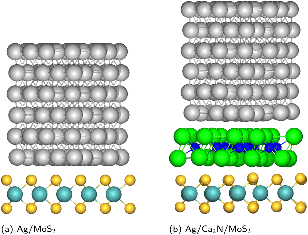 | ||
| Fig. 1 Geometries of metal/MoS2 and metal/Ca2N/MoS2 heterostructures, for the specific case of Ag. Mo: cyan; S: yellow; Ag: silver; Ca: green; N: blue. | ||
Semiconductor doping is an essential component of modern device engineering, but represents a challenge for 2D materials as the space in which to place dopant atoms is drastically reduced. MoS2 can be doped by substituting group-adjacent transition-metal atoms at the molybdenum sites (e.g. using rhenium for n-type doping16 and niobium for p-type doping17). However, this method can only mildly dope the semiconductor since the MoS2 would become an alloy at higher dopant concentrations, and the material properties that make it appealing for devices could be lost.
Importantly, metal/MoS2 interface properties, like gap-state formation and doping level, vary with respect to the choice of metal. In terms of previous computational studies, Gong et al.15 used the local density approximation (LDA) to correlate shifting of the MoS2 Fermi level with the work function of the metal. Another study from Kang et al.18 used the LDA paired with Grimme's D2 dispersion correction19 to propose three types of bonding between MoS2 or WeS2 and metal surfaces: (1) weak adhesion resulting from van der Waals contacts, (2) medium adhesion, and (3) strong adhesion facilitated by covalent bonds between the materials. Type 1 metals are predicted to lead to large tunneling barriers, while type 3 metals lead to the metallization of the semiconductor under the contact. However, we note that the LDA cannot be recommended for these types of calculations in general, or for pairing with a dispersion correction, due to its massive overbinding tendency.20,21 Other studies have also noted variation in contact properties with a variety of metals.22–24
An alternative to transition metals in metal/MoS2 contacts is to use the heavy pnictogens, antimony and bismuth. These materials have very low densities of electronic states near the Fermi level, making them appealing for use in contacts. Indeed, two recent experimental studies showed very low contact resistances for pnictogen/MoS2 heterostructures. Shen et al.25 found a contact resistance of 123 Ω μm between MoS2 and a bismuth (0001) surface, compared to typical values of ca. 1 kΩ μm.26 This was accompanied by a computational study of the Bi/MoS2 interface that used the PBE density functional,27 but neglected a dispersion correction, which is especially important for interfaces involving layered materials and for heavy, polarizable atoms like bismuth. Subsequently, Li et al.28 studied the antimony/MoS2 junction and found a minimum contact resistance of 42 Ω μm. They attributed this substantial improvement over the previous result for bismuth to the use of the (01![[1 with combining macron]](https://www.rsc.org/images/entities/char_0031_0304.gif) 2) surface of antimony, which exhibits better orbital overlap with MoS2 than the (0001) surface, for which larger contact resistances were measured.
2) surface of antimony, which exhibits better orbital overlap with MoS2 than the (0001) surface, for which larger contact resistances were measured.
Another vibrant area of research is using multiple 2D materials to construct heterostructures that exhibit emergent properties differing from those of their component monolayers. For example, various TMDCs may be combined to modify thermal conductance,29 and the electronic properties of an organic/MoS2 heterobilayer can be tuned by applied strain to enable photocatalytic water splitting.30 As with bulk layered materials, their heterostructures are typically bound by van der Waals interactions, which permits a wide variety of possible configurations.31
Compared to a bare metal/MoS2 heterostructure, the deposition of a heterobilayer onto a metal slab can be thought of as the insertion of an intermediate material between the metal and the semiconductor. Such insertion represents yet another alternative to improve contact properties across a metal/MoS2 interface. Notably, inserting a hexagonal boron nitride (h-BN) monolayer at a Co/MoS2 interface served to eliminate the gap states by preventing chemical interactions between the metal and MoS2.32–34 However, this device geometry produces a junction with van der Waals contacts, in which electron transport is limited by the tunneling barriers across the metal/h-BN/MoS2 junction. As expected, this leads to higher contact resistance (experimentally observed to be 3 kΩ μm), whereas a true Ohmic contact would be free of a tunneling barrier.
As an alternative to h-BN, several computational studies have considered 2D electrides as promising layered materials to insert at metal/MoS2 interfaces, as shown in Fig. 1(b). Electrides are a class of ionic solids, where electrons localized within interstitial voids act in the place of anions.35,36 For the specific case of 2D electrides, the anionic electrons are localized in the space between the positively charged layers.37,38 This gives rise to an electrostatic component to the interlayer binding, in addition to the van der Waals attraction, which leads to very large exfoliation energies and low thermal expansion coefficients.39,40 Analogous to other layered materials, 2D electrides may be exfoliated to their monolayers, which are known as electrenes.41,42
Electrene insertion at a metal/MoS2 contact has been predicted to create an interface that is free of tunneling and Schottky barriers.43,44 The latter is accomplished by the electrene donating its surface electrons to negatively dope the semiconductor, without inducing gap states. Several electrenes have been considered for this purpose, all belonging to the AE2Pn stoichiometry (AE = Ca, Sr, Ba; Pn = N, P, As, Sb). Rafiee Diznab et al.44 concluded that Ca2N was the optimal choice for metal/AE2Pn/MoS2 heterojunctions, owing to its large surface charge density. However, Tang45 noted that creating a Ca2N/MoTe2 heterobilayer causes the MoTe2 to undergo a transition from the semiconducting 1H phase to the metallic 1T′ phase, eliminating its utility as a semiconductor. A similar effect may be observed for Ca2N/MoS2 heterobilayers, and more research is needed to explore various AE2Pn/TMDC combinations to assess the 1H/1T′ phase stability. Finally, Rafiee Diznab et al.44 only considered gold and copper as contact metals and found that copper's smaller electronegativity allows more charge to be donated to MoS2 from the electrene. This opens the door to variation of the metal/Ca2N/MoS2 contact properties depending on the identity of the metal.
In this work, we explore the interface properties of metal/Ca2N/MoS2 heterostructures with six metals: gold, silver, copper, ruthenium, molybdenum, and tungsten. We also consider metal/MoS2 interfaces for all of these listed metals, along with yttrium, platinum, antimony, and bismuth, for comparison. Key interface properties that inform contact resistance are computed using dispersion-corrected density-functional theory (DFT) and the results compared across all heterostructure types.
2 Computational methods
2.1 DFT calculations
Metal/MoS2 and metal/Ca2N/MoS2 heterostructures were constructed from their composite materials using the vaspkit package46 to generate a commensurate cell with a biaxial strain, ε, applied to one of the materials. The in-plane lattice constants of MoS2 were kept fixed at their relaxed value of 3.17 Å and those of the other materials were strained to form a commensurate cell. Generally, heterostructures were chosen based on minimizing both the strain on the non-semiconductor materials and the number of atoms in the structure. The unit cell a-parameter of each individual material was optimized with Quantum ESPRESSO,47,48 using the DFT methods detailed below, before the construction of the heterostructures to assess the strain. The final, optimized heterostructure geometries, along with the numbers of formula units, percent strains, and strain energies for each component material, are given in Tables S1 and S2 of the ESI.† To evaluate the strain energy, the atomic positions of the Ca2N and metals were relaxed, subject to fixed lattice constants corresponding to the heterostructure geometries. The strain energy is then the energy difference between these fixed-lattice-constant structures and the results of full geometry relaxation with optimum a lattice parameters. A 20 Å vacuum spacing in the z-direction was applied in all calculations to isolate the heterostructures (or the constituent materials) from their periodic images. This value aligns with previous work,44,49 and a convergence plot for the vacuum spacing is shown in Fig. S1 of the ESI.†All calculations were performed using the PBE exchange–correlation functional27 and the exchange-hole dipole moment (XDM) dispersion model.50–52 PBE-XDM has previously shown strong accuracy compared to experiment or higher-level theory for properties of bulk TMDCs,53 bulk layered electrides,40 and bulk metals,54 although there has yet to be any benchmarking for the heterostructures of these materials due to the lack of any available reference data.
To improve computational efficiency, the geometry relaxations of the heterostructures were handled in two steps. The first was a coarse relaxation with the Fritz-Haber Institute ab initio materials simulations (FHIaims) package55 with lightdense numerical atom-centered orbital basis sets. Relativistic effects were treated with the zeroth-order regular approximation56 (ZORA). The k-point grids used a Monkhost–Pack scheme,57 with the number of points along the reciprocal lattice vector, bi, chosen according to58
| ni = int[max(1,Rk|bi| + 0.5)], | (1) |
For each heterostructure, the MoS2 Löwdin-projected62 density of states (DOS) was computed. The ESI† shows both the “in-heterostructure” DOS, where the MoS2 is in contact with the metal or Ca2N, and the “distorted” DOS of an isolated MoS2 monolayer with the geometric distortions induced by the contact retained. The “pristine” DOS of an isolated MoS2 monolayer at its fully relaxed geometry was also computed for comparison. A Gaussian smearing of 0.1 eV was applied in each case.
Several other interface properties were computed, including the sum of ionic and Hartree potentials and the all-electron and valence densities. The sum of ionic and Hartree potentials, when averaged over the xy plane, is informative about tunneling properties at the interfaces. The all-electron and valence densities were used to compute atomic charges and charge transfer within Bader's quantum theory of atoms in molecules (QTAIM).63,64 The Bader atomic charges were computed using the Yu-Trinkle algorithm,65 implemented in the critic2 software package.66
2.2 Metrics
In this section, we define several metrics used to describe the structural and electronic properties of the heterojunctions, all of which were evaluated using the QE-relaxed geometries. First, we consider three structural properties, beginning with the average out-of-plane distance between the MoS2 and metal surface for the metal/MoS2 interfaces:Δ![[z with combining macron]](https://www.rsc.org/images/entities/i_char_007a_0304.gif) S–metal = |S − metal|. S–metal = |S − metal|. | (2) |
S is the average vertical, z, position of the S atoms in contact with the metal, while metal is the average z position of the surface metal atoms. This descriptor also implies a standard deviation in the difference between the two sets of z positions, σS–metal, which neatly describes the distortion at the interface.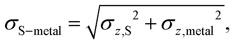 | (3) |
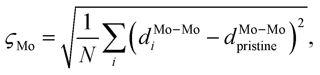
Here, σz,S2 is the variance of the z positions of the contact sulfurs, and σz,metal2 is the variance of the z positions of the atoms forming the metal surface. Finally, a honeycomb distortion of the MoS2 was observed for some interfaces. It can be quantified by comparing the bonded Mo–Mo distances in the distorted structure to the Mo–Mo distance in pristine MoS2 using a root-mean square. This RMS distortion of the Mo atoms is
 | (4) |
In terms of electronic properties, the tunneling barrier height (TBH) and width (TBW) are computed from the sum of the ionic and Hartree potentials of the interface averaged over the xy-plane, as in previous work.44 Plots of this averaged potential, V, versus the vertical, z, direction, are shown in the ESI.† The TBH is defined as the maximum averaged potential at the interface, relative to the Fermi energy, while the TBW is the z distance between the two intersections of the averaged potential with the Fermi energy. The extent of charge transfer resulting from interface formation, QMoS2, was also computed by summing the MoS2 charges in the heterostructure over the unit cell, and expressing the result per formula unit.
Another important consideration is the band gap of the semiconductor. Even in cases where gap state formation is not a problem, the band gap of MoS2 can be altered with the application of strain67 or charge (vide infra). Here, the band gap is estimated from the edges of the MoS2 in-heterostructure DOS and is important for understanding the impact of the geometric structure on the electronic structure.
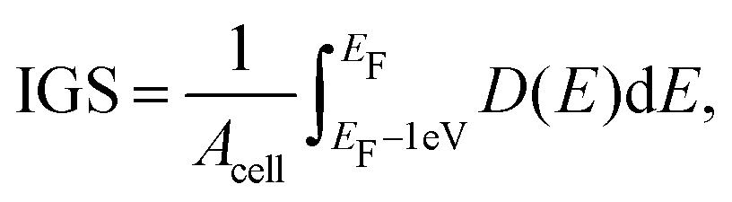
With the formation of gap states in the semiconductor comes Fermi level pinning,68 which can lead to a Schottky barrier and a high contact resistance. As the formation of gap states is difficult to quantify, we introduce a metric termed the integrated gap states (IGS). The IGS is defined as
 | (5) |
Finally, the exfoliation energy of an interface is defined as
 | (6) |
3 Results and discussion
3.1 Metal/MoS2 interfaces
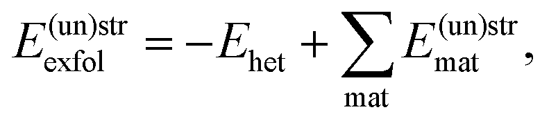
Table S1 and Fig. S2–S4 of the ESI† provide the full computational results for the metal/MoS2 heterostructures. As discussed in previous literature studying the metal/MoS2 interface, variation in the interface properties can be observed depending on the metal species in contact with the MoS2. A contributing factor to this is the type of bonding between the two materials, spanning a spectrum between covalent and van der Waals bonding. The interaction of each metal with MoS2 falls somewhere on this spectrum, which in turn will inform its interface characteristics. A simple metric with which to draw this spectrum is the average z distance between the metal and the MoS2. As van der Waals forces are fairly weak in nature, a large ΔS–metal spacing will be observed if this interaction dominates. By contrast, covalent binding is very strong, and will act to pull the two materials together, leading to a small ΔS–metal. Within each interaction class, the particular atomic radii will also contribute to the interlayer spacing (i.e. Mo < W and Cu < Ag < Au).
An extension of the ΔS–metal distance metric is its standard deviation, σS–metal. Weak van der Waals (vdW) forces will not easily distort the MoS2 (or metal surface), so σS–metal should be fairly small. On the other hand, covalent bonds can distort the structures of both the metal and MoS2 at the interface to optimise the orbital overlap, leading to a large σS–metal. The trend of large-Δz/small-σ and small-Δz/large-σ can be seen in the upper left plot in Fig. 2(a), which correlates the two metrics. Using a combination of these geometric results and the projected DOS results in the ESI,† we group the metals into three categories to describe their binding to MoS2: covalent (molybdenum, tungsten, yttrium), intermediate (copper, silver, ruthenium, platinum), and vdW (gold, antimony, bismuth). These groupings align well with the results reported by Kang et al.,18 who identified molybdenum and tungsten as type 3 (strong bonding), palladium (a platinum-group metal) as type 2 (intermediate), and gold as type 1 (weak bonding).
 | ||
| Fig. 2 Variation of selected quantities for metal/MoS2 heterostructures as a function of the average S–metal contact distance, ΔS–metal. (a) Standard deviation in the S–metal distance, σS–metal; (b) integrated gap states, IGS; (c) Bader charge transfer to the MoS2, QMoS2; and (d) tunneling barrier height, TBH. Data points are coloured according to the predicted metal–MoS2 interaction type: covalent = green, intermediate = black, van der Waals = purple. | ||
In the present work, assignment of the interactions as vdW, intermediate, or covalent bonding is based on decomposing the exfoliation energies into contributions from the base density functional (PBE) and the dispersion energy (see Table S3, ESI†). Cases with only vdW binding have repulsive base-functional components, intermediate cases have positive base-functional components that are smaller in magnitude than the dispersion contributions, and cases with covalent bonding have base-functional contributions that are larger in magnitude than the dispersion binding. The only exception is Mo/MoS2, which would be intermediate by this descriptor; however, it is classed as exhibiting covalent bonding due to the computed electrostatic potential in Fig. S4 (ESI†).
The distinction between strong and weak binding is also apparent from consideration of the charge transfer, which is plotted as a function of ΔS–metal in Fig. 2(c). Due to the difference in electronegativies, charge is universally donated from the metal to the MoS2, although the amount of charge transferred across the covalently bound interfaces is much greater than for the vdW interfaces. The somewhat anomalous results for yttrium and platinum can be explained by their very small and large work functions,69 respectively, compared to the other metals considered. The ease of liberating an electron from the metal plays an apparent role in the extent of charge transferred to the MoS2.
The ΔS–metal distance also roughly correlates with the extent of metallization of the semiconductor, quantified by our IGS metric, as shown in Fig. 2(b). Metals that form van der Waals interfaces, like Sb and Bi, cause minimal gap state formation, while molybdenum and tungsten fully metalize the semiconductor. The low IGS highlights the reason for the good transport performance of the pnictogens, where the small DOS within the gap region prevents extensive Fermi-level pinning and results in minimal contact resistance. Even a slight increase in the metallic DOS can lead to an appreciable Schottky barrier, as in the cases of Cu, Ag, and Au. Band structures for three representative cases (Bi(0001), Ag, and Mo) are presented in Fig. S5 (ESI†). Here, Bi(0001)/MoS2 shows a Fermi level pinned very close to the MoS2 conduction band, suggesting a low Schottky barrier, while the formation of gap states in Ag/MoS2 lead to pinning inside the band gap. The band structure of Y/MoS2 shows that the band edges of MoS2 are highly mixed with yttrium states, highlighting the metallization seen in that heterostructure. However, Kang et al.18 argue that metallization of the MoS2 can serve to ease transport of carriers into its conduction band, provided this only occurs under the metal contact. That said, the large geometric distortion of the MoS2 monolayer due to covalent bonding with the metal may lead to instability away from the contact.
Finally, as the intermaterial separation shrinks, the tunneling barrier across the interface should as well. Indeed, this correlation is evident from the plot of TBH as a function of ΔS–metal in Fig. 2(d), where a sigmoid-like trend is visible. This points to the limit of infinite separation at large Δ, where the potential approaches the vacuum level, and the limit of high orbital overlap at small Δ. Covalent bonding is particularly conducive to facile electron tunneling, with the in-plane average potential at the interface being below the Fermi level for Mo, W, Y, and Ru. As shown in Fig. S4 (ESI†), all of the transition metals have some local areas at the interface where the potential dips below the Fermi level, suggesting tunneling-free transport. However, no such areas are observed for the heavy pnictogens in either orientation. The tunneling barriers for the pnictogen semimetals come from minimal chemical interactions between the materials, which also results in low Schottky barriers. This is similar to the Co/h-BN/MoS2 interface,32,34 although the presence of only a single interface region (compared to both the Co/h-BN and h-BN/MoS2 interfaces) leads to smaller tunneling barriers for Sb/MoS2 and Bi/MoS2.
To summarize the results for the metal/MoS2 heterostructures in brevi, the interfacial interactions span a broad range, with weak van der Waals forces and strong covalent bonding as the two extremes. vdW interfaces are defined by a large intermaterial separation, which leads to minimal distortion and charge transfer. This has the consequence of minimal gap-state formation, but large tunneling barriers. By contrast, covalent interfaces, defined by a small intermaterial separation, show large distortions and substantial charge transfer. This results in minimal tunneling barriers, but a greater extent of metallization of the semiconductor.
3.2 Ca2N/MoS2 interfaces
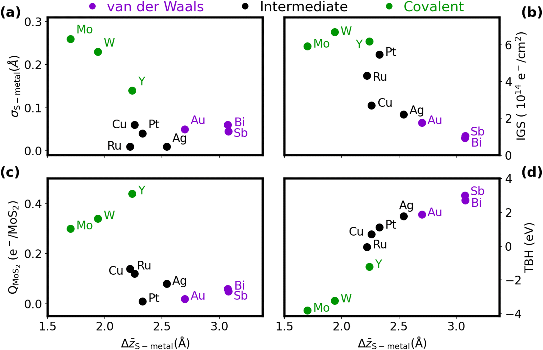
A variety of Ca2N/MoS2 heterobilayers (denoted A–E, see Table S4, ESI†) were considered in preparation for constructing the metal/Ca2N/MoS2 interfaces. Here, we will focus on the two containing the fewest numbers of atoms in the unit cell, henceforth labeled “Geometry A” (48 atoms) and “Geometry B” (21 atoms), which also involve the least Ca2N lattice strain. As summarised in Table S4 (ESI†), a very similar amount of charge per formula unit is transferred from the electron-rich Ca2N to the MoS2 in each case, and the intermaterial separations are nearly identical. The prominant difference between these two geometries is that the MoS2 has a band gap of 1.3 eV in Geometry A, which shrinks to 0.5 eV in Geometry B. This can be seen from the MoS2-projected DOS of each interface, as plotted in Fig. 3. Different rotations of the Ca2N layer within each heterostructure did not yield differences in the band gap.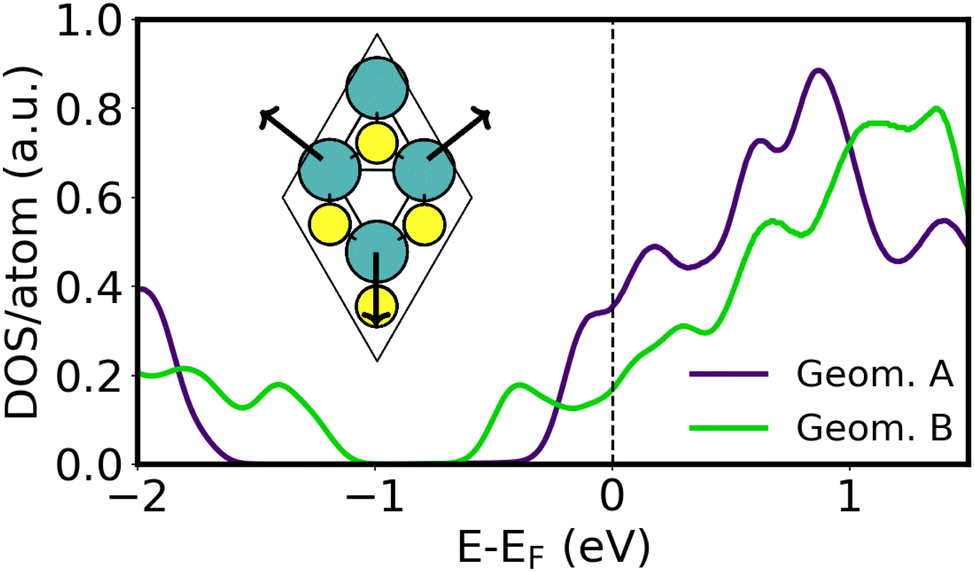 | ||
| Fig. 3 MoS2-projected DOS for the two selected Ca2N/MoS2 interface geometries. The computed DOS is divided by the total number of atoms in the heterobilayer due to the differing unit-cell sizes. The inset shows the honeycomb distortion present in Geometry B. | ||
The present results are reminiscent of the work of Castellanos-Gomez et al.,67 where strain is used to tune the MoS2 band gap. However, the lattice constants in Geometries A and B are exact integer multiples of those for the pristine MoS2 unit cell (viz. 3 and 2, respectively), so no strain is directly applied. While strain is applied to the Ca2N monolayer, it amounts to only 0.1% and 1.7% for Geometries A and B, respectively. With an energy difference of only 0.8 meV Å−1 in favour of Geometry A, the two structures are nearly degenerate due to the slightly greater strained exfoliation energy of Geometry B, which partly offsets its 1.4 meV Å−1 strain energy.
The band gap shrinking in Geometry B was traced to a distortion of the MoS2 honeycomb, as shown in the inset of Fig. 3, where the Mo atoms move away from the hexagonal void at the centre of the unit cell. This creates local environments with alternating short and long Mo–Mo distances, similar to those seen in strained MoS2. The extent of this honeycomb distortion is quantified using the ςMo metric, which is 0.04 Å for Geometry A and increases to 0.19 Å for Geometry B. The structural distortion and consequent band gap shrinking may be the beginning of a 1H → 1T′ phase transition, previously noted by Tang.45 As shown in Table S4 (ESI†), Geometries C–E have ςMo of 0.13–0.15 Å and shrunken MoS2 band gaps ranging from 0.6–0.9 eV. The ςMo metric was also evaluated for all of the metal/MoS2 heterostructures (see Table S1, ESI†) and was found to range from 0–0.04 Å for most metals. The one exception to this was for Y/MoS2, where ςMo reaches a large value of 0.18 Å, similar to that seen for Geometry B.
The source of the honeycomb distortion seen in Geometries B–E of the Ca2N/MoS2 interface and the Y/MoS2 interface can be traced in part to symmetry breaking in the particular heterostructure geometry. As a simple visual comparison, Fig. 4 shows a top view of the Pt/MoS2 and Y/MoS2 heterostructures, which are chosen due to their small unit cells. In the Pt/MoS2 case, minimal honeycomb distortion is observed as the overlap of the MoS2 with the Pt surface is such that all Mo atoms are in very similar geometric environments. However, in the Y/MoS2 case, the lattice alignment means that Mo and S atoms either lie directly above a Y–Y bond at the surface, or lie above a hexagonal vacancy between six Y atoms. This symmetry breaking induces the MoS2 honeycomb distortion.
 | ||
| Fig. 4 Structures of the Pt/MoS2 and Y/MoS2 interfaces. Mo: cyan; S: yellow; Pt silver; Y: grey. | ||
In addition to poor honeycomb overlap, extensive charge donation to a MoS2 monolayer is also able to induce a honeycomb distortion. This can be seen in Fig. 5 for the case of a negatively charged 4 × 4 × 1 MoS2 supercell. Here, the tot_charge keyword in QE was used to inject a fixed amount of charge into the MoS2 supercell, while applying a uniform background counter charge.70 The atomic positions of the charged structure were then relaxed using only the Γ point, with kinetic energy and density cutoffs of 80 and 800 Ry, respectively. The results in Fig. 5 show that, when enough charge is applied to the isolated monolayer, the honeycomb distortion again becomes spontaneous. However, at the charge transfer levels observed for the Ca2N/MoS2 interfaces in this work (viz. 0.01–0.44 e−/MoS2), isolated MoS2 does not distort. Therefore, we conclude that it is the combination of high charge transfer to MoS2 and distinctly different Mo environments induced by contact with the Ca2N or metal surface that leads to the honeycomb distortion. This is a combination that is present for Y/MoS2, as well as for Geometries B-E of the Ca2N/MoS2 heterostructures. Geometry A, which was used in our previous studies of Ca2N/MoS2 and metal/Ca2N/MoS2 interfaces43,44 due to the better lattice-constant match, is the rare exception where the nearly symmetric honeycomb overlap of the heterobilayer is adequate to prevent the distortion.
 | ||
| Fig. 5 Extent of the honeycomb distortion, ςMo, as a function of the negative charge per formula unit applied to a 4 × 4 × 1 supercell of monolayer MoS2. | ||
3.3 Metal/Ca2N/MoS2 interfaces
To interrogate the role of the metal in metal/Ca2N/MoS2 interfaces, we constructed heterostructures where the MoS2 lattice constants are fixed and the strain placed on the Ca2N and metal slab is minimized, analogous to our metal/MoS2 calculations. Although Cu/Ca2N/MoS2 and Au/Ca2N/MoS2 have already been studied in the literature by Rafiee Diznab et al.,44 those structures were relaxed using PBE-D3BJ,71,72 which predicts slightly different intermaterial spacings and lattice constants (and therefore a different strain on Au or Cu) than PBE-XDM. For the sake of consistency, we constructed distinct heterostructures for this work. See Table S2 and Fig. S6–S8 of the ESI† for the full computational results for the metal/Ca2N/MoS2 heterostructures.Fig. 6(a) shows the band gap of MoS2 plotted against the ςMo metric for all the structures considered. All of the structures exhibit a significant MoS2 honeycomb distortion and, consequently, low band gaps. None of the metals considered have lattice parameters that are commensurate with Geometry A, which is the only heterobilayer considered to not exhibit band gap lowering. If Geometry A is enforced in a heterostructure at the cost of a larger strain on the metal, a large band gap is consistently observed (see Table S5, ESI†), as in our previous calculations involving Cu and Au.44 This shows that the metal's influence on the degree of the MoS2 honeycomb distortion, and the resultant band gap shrinking, is weak compared to the choice of heterobilayer.
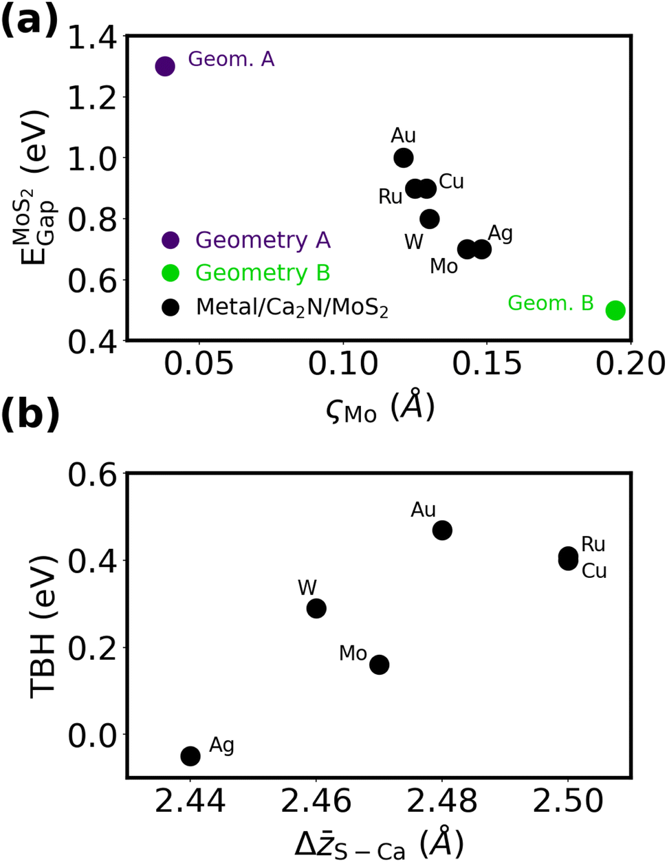 | ||
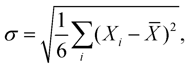
| Fig. 6 (a) MoS2 band gaps in metal/Ca2N/MoS2 heterostructures as a function of the honeycomb distortion; results for two Ca2N/MoS2 heterobilayers are included for comparison. (b) Ca2N/MoS2 tunneling barrier heights in metal/Ca2N/MoS2 heterostructures as a function of the average vertical S–Ca separation. | ||
Fig. 6(b) shows the TBH as a function of the electrene–MoS2 interlayer separation, ΔS–Ca. It is important to note the very much smaller y-axis interval in Fig. 6(b) compared to Fig. 2(d). All of the metal/Ca2N/MoS2 structures have low TBHs in the range of ca. 0 eV (Ag) to 0.5 eV (Au), compared to the range of ca. −4 eV (Mo) to 2 eV (Au) seen for the metal/MoS2 interfaces without the electrene.
Generally, for the metal/Ca2N/MoS2 heterostructures, the variation in interface metrics is very small across the six metals considered. This stands in stark contrast to the metal/MoS2 interfaces considered in Subsection 3.1, where different metal species lead to drastically different interface metrics. Exact quantities can be found in Table S1 (metal/MoS2) and Table S2 (metal/Ca2N/MoS2) (ESI†). As formation of gap states is not an issue for the metal/Ca2N/MoS2 interfaces,44 the IGS metric is not reported. The variability of the interface metrics with the choice of metal can be compared using the standard deviation, σ:
 | (7) |
![[X with combining macron]](https://www.rsc.org/images/entities/i_char_0058_0304.gif) is the average value of that metric for the six metals. Table 1 shows that, on average, the standard deviation of metal/MoS2 interface metrics is more than 10 times greater than that of metal/Ca2N/MoS2 interface metrics. Therefore, electrene insertion serves to lessen substantially the influence of the metal compared to metal/MoS2 interfaces, meaning that any of the metals considered could potentially be used in semiconductor devices involving metal/Ca2N/MoS2 heterojunctions.
is the average value of that metric for the six metals. Table 1 shows that, on average, the standard deviation of metal/MoS2 interface metrics is more than 10 times greater than that of metal/Ca2N/MoS2 interface metrics. Therefore, electrene insertion serves to lessen substantially the influence of the metal compared to metal/MoS2 interfaces, meaning that any of the metals considered could potentially be used in semiconductor devices involving metal/Ca2N/MoS2 heterojunctions.
| Interface | Standard deviation | |||
|---|---|---|---|---|
| Δz (Å) | σ S–metal (Å) | Q MoS2 (e−/MoS2) | TBH (eV) | |
| Metal/MoS2 | 0.37 | 0.11 | 0.13 | 2.48 |
| Metal/Ca2N/MoS2 | 0.02 | <0.01 | 0.02 | 0.20 |
4 Conclusions
The results presented here illustrate the ability of a metal to influence the interface properties of metal/MoS2 and metal/Ca2N/MoS2 heterostructures. In metal/MoS2 heterostructures, there is great variation in the interface metrics considered (Δz, σS–metal, QMoS2, and TBH), showing a strong dependence on the choice of metal. This variation can be characterized by placing metals on a spectrum, from van der Waals to covalent, that describes their interactions with MoS2. In contrast, the variation for metal/Ca2N/MoS2 interfaces is very small, indicating that the ability of a metal to influence the interface metrics is lessened by electrene insertion. We also note that in cases of large charge transfer to MoS2, paired with symmetry breaking at the interface, a honeycomb distortion takes place that shrinks the MoS2 band gap. The weak influence of the metal opens the door to a multitude of possible metal/electrene/TMDC interfaces for use in semiconductor devices. Because of this, other factors such as cost, sustainability, and viability in manufacturing should lead the discussion of what is the optimal choice.Data availability
The data that support this study are provided in this article and its accompanying ESI.†Conflicts of interest
The authors have no conflicts to disclose.Acknowledgements
The authors thank the Natural Sciences and Engineering Council (NSERC) of Canada and the Semiconductor Research Corporation (SRC) for financial support, as well as ACENET and the Digital Research Alliance of Canada for computational resources.References
- W. Choi, N. Choudhary, G. H. Han, J. Park, D. Akinwande and Y. H. Lee, Mater. Today, 2017, 20, 116–130 CrossRef CAS.
- S. Manzeli, D. Ovchinnikov, D. Pasquier, O. V. Yazyev and A. Kis, Nat. Rev. Mater., 2017, 2, 1–15 Search PubMed.
- G. E. Moore, Proc. IEEE, 1998, 86, 82–85 Search PubMed.
- D. Gupta, V. Chauhan and R. Kumar, Inorg. Chem. Commun., 2020, 121, 108200 CrossRef CAS.
- Y. Venkata Subbaiah, K. Saji and A. Tiwari, Adv. Funct. Mater., 2016, 26, 2046–2069 CrossRef CAS.
- S. A. Han, R. Bhatia and S.-W. Kim, Nano Convergence, 2015, 2, 1–14 CrossRef.
- J. Strachan, A. F. Masters and T. Maschmeyer, ACS Appl. Energy Mater., 2021, 4, 7405–7418 CrossRef CAS.
- L. Liu, J. Wu, L. Wu, M. Ye, X. Liu, Q. Wang, S. Hou, P. Lu, L. Sun and J. Zheng, et al. , Nat. Mater., 2018, 17, 1108–1114 CrossRef CAS PubMed.
- K. F. Mak, C. Lee, J. Hone, J. Shan and T. F. Heinz, Phys. Rev. Lett., 2010, 105, 136805 CrossRef PubMed.
- Y.-C. Lin, D. O. Dumcenco, Y.-S. Huang and K. Suenaga, Nat. Nanotechnol., 2014, 9, 391–396 CrossRef CAS PubMed.
- Y. Yu, G.-H. Nam, Q. He, X.-J. Wu, K. Zhang, Z. Yang, J. Chen, Q. Ma, M. Zhao and Z. Liu, et al. , Nat. Chem., 2018, 10, 638–643 CrossRef CAS PubMed.
- D. S. Schulman, A. J. Arnold and S. Das, Chem. Soc. Rev., 2018, 47, 3037–3058 RSC.
- A. Allain, J. Kang, K. Banerjee and A. Kis, Nat. Mater., 2015, 14, 1195–1205 CrossRef CAS PubMed.
- T. Shen, J.-C. Ren, X. Liu, S. Li and W. Liu, J. Am. Chem. Soc., 2019, 141, 3110–3115 CrossRef CAS PubMed.
- C. Gong, L. Colombo, R. M. Wallace and K. Cho, Nano Lett., 2014, 14, 1714–1720 CrossRef CAS PubMed.
- R. Torsi, K. T. Munson, R. Pendurthi, E. Marques, B. Van Troeye, L. Huberich, B. Schuler, M. Feidler, K. Wang and G. Pourtois, et al. , ACS Nano, 2023, 17, 15629–15640 CrossRef CAS PubMed.
- M. R. Laskar, D. N. Nath, L. Ma, E. W. Lee, C. H. Lee, T. Kent, Z. Yang, R. Mishra, M. A. Roldan and J.-C. Idrobo, et al. , Appl. Phys. Lett., 2014, 104, 092104 CrossRef.
- J. Kang, W. Liu, D. Sarkar, D. Jena and K. Banerjee, Phys. Rev. X, 2014, 4, 031005 CAS.
- S. Grimme, J. Comput. Chem., 2006, 27, 1787–1799 CrossRef CAS PubMed.
- T. Björkman, A. Gulans, A. Krasheninnikov and R. Nieminen, J. Condens. Matter Phys., 2012, 24, 424218 CrossRef PubMed.
- H. L. Schmider and A. D. Becke, J. Chem. Phys., 1998, 108, 9624–9631 CrossRef CAS.
- I. Popov, G. Seifert and D. Tománek, Phys. Rev. Lett., 2012, 108, 156802 CrossRef PubMed.
- H. Zhong, R. Quhe, Y. Wang, Z. Ni, M. Ye, Z. Song, Y. Pan, J. Yang, L. Yang and M. Lei, et al. , Sci. Rep., 2016, 6, 21786 CrossRef CAS PubMed.
- S. McDonnell, C. Smyth, C. L. Hinkle and R. M. Wallace, ACS Appl. Mater. Interfaces, 2016, 8, 8289–8294 CrossRef CAS PubMed.
- P.-C. Shen, C. Su, Y. Lin, A.-S. Chou, C.-C. Cheng, J.-H. Park, M.-H. Chiu, A.-Y. Lu, H.-L. Tang and M. M. Tavakoli, et al. , Nature, 2021, 593, 211–217 CrossRef CAS PubMed.
- M. Chhowalla, D. Jena and H. Zhang, Nat. Rev. Mater., 2016, 1, 1–15 Search PubMed.
- J. P. Perdew, K. Burke and M. Ernzerhof, Phys. Rev. Lett., 1996, 77, 3865 CrossRef CAS PubMed.
- W. Li, X. Gong, Z. Yu, L. Ma, W. Sun, S. Gao, Ç. Köroglu, W. Wang, L. Liu and T. Li, et al. , Nature, 2023, 613, 274–279 CrossRef CAS PubMed.
- S. Xu, P. Wu and Y. Chen, Comput. Mater. Sci., 2024, 245, 113282 CrossRef CAS.
- S. K. Das, L. Patra, P. Samal and P. K. Sahoo, ACS Appl. Electron. Mater., 2024, 6, 1415–1423 CrossRef CAS.
- J. Celis and W. Cao, J. Chem. Theory Comput., 2024, 20, 2377–2389 CrossRef CAS PubMed.
- M. Farmanbar and G. Brocks, Phys. Rev. B:Condens. Matter Mater. Phys., 2015, 91, 161304 CrossRef.
- J. Wang, Q. Yao, C.-W. Huang, X. Zou, L. Liao, S. Chen, Z. Fan, K. Zhang, W. Wu and X. Xiao, et al. , Adv. Mater., 2016, 28, 8302–8308 CrossRef CAS PubMed.
- X. Cui, E.-M. Shih, L. A. Jauregui, S. H. Chae, Y. D. Kim, B. Li, D. Seo, K. Pistunova, J. Yin and J.-H. Park, et al. , Nano Lett., 2017, 17, 4781–4786 CrossRef CAS PubMed.
- J. L. Dye, Acc. Chem. Res., 2009, 42, 1564–1572 CrossRef CAS PubMed.
- S. G. Dale and E. R. Johnson, J. Phys. Chem. A, 2018, 122, 9371–9391 CrossRef CAS PubMed.
- K. Lee, S. W. Kim, Y. Toda, S. Matsuishi and H. Hosono, Nature, 2013, 494, 336–340 CrossRef CAS PubMed.
- X. Zhang, Z. Xiao, H. Lei, Y. Toda, S. Matsuishi, T. Kamiya, S. Ueda and H. Hosono, Chem. Mater., 2014, 26, 6638 CrossRef CAS.
- S. G. Dale and E. R. Johnson, Phys. Chem. Chem. Phys., 2017, 19, 27343–27352 RSC.
- A. F. Rumson and E. R. Johnson, J. Chem. Phys., 2023, 159, 174701 CrossRef CAS PubMed.
- D. L. Druffel, K. L. Kuntz, A. H. Woomer, F. M. Alcorn, J. Hu, C. L. Donley and S. C. Warren, J. Am. Chem. Soc., 2016, 138, 16089–16094 CrossRef CAS PubMed.
- D. L. Druffel, A. H. Woomer, K. L. Kuntz, J. T. Pawlik and S. C. Warren, J. Mater. Chem. C, 2017, 5, 11196–11213 RSC.
- F. Kaadou, J. Maassen and E. R. Johnson, J. Phys. Chem. C, 2021, 125, 11656–11664 CrossRef CAS.
- M. R. Diznab, A. F. Rumson, J. Maassen and E. R. Johnson, Phys. Chem. Chem. Phys., 2024, 26, 16947–16954 RSC.
- Q. Tang, ChemPhysChem, 2019, 20, 595–601 CrossRef CAS PubMed.
- V. Wang, N. Xu, J.-C. Liu, G. Tang and W.-T. Geng, Comput. Phys. Commun., 2021, 267, 108033 CrossRef CAS.
- P. Giannozzi, O. Andreussi, T. Brumme, O. Bunau, M. B. Nardelli, M. Calandra, R. Car, C. Cavazzoni, D. Ceresoli and M. Cococcioni, et al. , J. Phys.: Condens. Matter, 2017, 29, 465901 CrossRef CAS PubMed.
- P. Giannozzi, O. Baseggio, P. Bonfà, D. Brunato, R. Car, I. Carnimeo, C. Cavazzoni, S. De Gironcoli, P. Delugas and F. Ferrari Ruffino, et al. , J. Chem. Phys., 2020, 152, 154105 CrossRef CAS PubMed.
- M. R. Diznab, E. R. Johnson and J. Maassen, Nanoscale, 2023, 26, 16947–16954 Search PubMed.
- E. R. Johnson, in Non-covalent Interactions in Quantum Chemistry and Physics, ed. A. Otero-de-la-Roza and G. A. DiLabio, Elsevier, 2017, ch. 5, pp. 169–194 Search PubMed.
- A. Otero-de-la-Roza and E. R. Johnson, J. Chem. Phys., 2012, 136, 174109 CrossRef CAS PubMed.
- A. J. A. Price, A. Otero-de-la-Roza and E. R. Johnson, Chem. Sci., 2023, 14, 1252–1262 RSC.
- A. Otero-de-la-Roza, L. M. LeBlanc and E. R. Johnson, J. Phys. Chem. Lett., 2020, 11, 2298–2302 CrossRef CAS PubMed.
- A. A. Adeleke and E. R. Johnson, Phys. Rev. B, 2023, 107, 064101 CrossRef CAS.
- V. Blum, R. Gehrke, F. Hanke, P. Havu, V. Havu, X. Ren, K. Reuter and M. Scheffler, Comput. Phys. Commun., 2009, 180, 2175–2196 CrossRef CAS.
- E. van Lenthe, E.-J. Baerends and J. G. Snijders, J. Chem. Phys., 1994, 101, 9783–9792 CrossRef CAS.
- H. J. Monkhorst and J. D. Pack, Phys. Rev. B, 1976, 13, 5188–5192 CrossRef.
- https://www.vasp.at/wiki/index.php/KPOINTS, See this resouce for information on the Rk parameter for k-spacings.
- A. Dal Corso, Comput. Mater. Sci., 2014, 95, 337–350 CrossRef CAS.
- M. Methfessel and A. Paxton, Phys. Rev. B:Condens. Matter Mater. Phys., 1989, 40, 3616 CrossRef CAS PubMed.
- J. D. Head and M. C. Zerner, Chem. Phys. Lett., 1985, 122, 264–270 CrossRef CAS.
- P.-O. Löwdin, J. Chem. Phys., 1950, 18, 365–375 CrossRef.
- R. F. Bader, Acc. Chem. Res., 1985, 18, 9–15 CrossRef CAS.
- P. L. A. Popelier, in The Chemical Bond: Fundamental Aspects of Chemical Bonding, ed. G. Frenking and S. Shaik, Wiley, 2014, ch. 8, pp. 271–308 Search PubMed.
- M. Yu and D. R. Trinkle, J. Chem. Phys., 2011, 134, 064111 CrossRef PubMed.
- A. Otero-de-la Roza, E. R. Johnson and V. Luaña, Comput. Phys. Commun., 2014, 185, 1007–1018 CrossRef CAS.
- A. Castellanos-Gomez, R. Roldán, E. Cappelluti, M. Buscema, F. Guinea, H. S. Van Der Zant and G. A. Steele, Nano Lett., 2013, 13, 5361–5366 CrossRef CAS PubMed.
- K. Sotthewes, R. Van Bremen, E. Dollekamp, T. Boulogne, K. Nowakowski, D. Kas, H. J. Zandvliet and P. Bampoulis, J. Phys. Chem. C, 2019, 123, 5411–5420 CrossRef CAS PubMed.
- CRC handbook of chemistry and physics, ed. W. M. Haynes, CRC Press, London, England, 97th edn, 2016 Search PubMed.
- G. Makov and M. C. Payne, Phys. Rev. B:Condens. Matter Mater. Phys., 1995, 51, 4014 CrossRef CAS PubMed.
- S. Grimme, J. Antony, S. Ehrlich and H. Krieg, J. Chem. Phys., 2010, 132, 154104 CrossRef PubMed.
- S. Grimme, S. Ehrlich and L. Goerigk, J. Comput. Chem., 2011, 32, 1456–1465 CrossRef CAS PubMed.
Footnote |
| † Electronic supplementary information (ESI) available: structural and electronic properties of all interfaces; visualizations of the atomic structures, tabulated metrics, selected band structures, DOS plots, and plane-averaged potential plots. See DOI: https://doi.org/10.1039/d4cp04577g |
| This journal is © the Owner Societies 2025 |