
Light radiation annealing enables unidirectional crystallization of vacuum-assisted Sn–Pb perovskites for efficient tandem solar cells†
Ciyu
Ge
 a,
Qi
Xu
a,
Dayu
Liu
a,
Wenjiang
Ye
a,
Yongxin
Zhu
a,
Peiyan
Zhang
a,
Jiakuan
Yang
b,
Guangxing
Liang
c,
Ling
Xu
a,
Ying
Zhou
ad,
Haisheng
Song
a,
Chao
Chen
*ade and
Jiang
Tang
*ade
a,
Qi
Xu
a,
Dayu
Liu
a,
Wenjiang
Ye
a,
Yongxin
Zhu
a,
Peiyan
Zhang
a,
Jiakuan
Yang
b,
Guangxing
Liang
c,
Ling
Xu
a,
Ying
Zhou
ad,
Haisheng
Song
a,
Chao
Chen
*ade and
Jiang
Tang
*ade
aWuhan National Laboratory for Optoelectronics (WNLO) and School of Optical and Electronic Information (SOEI), Huazhong University of Science and Technology, Wuhan, 430074, China. E-mail: jtang@mail.hust.edu.cn; cchen@hust.edu.cn
bSchool of Environmental Science and Engineering, Huazhong University of Science and Technology, Wuhan, 430074, China
cState Key Laboratory of Radio Frequency Heterogeneous Integration College of Physics and Optoelectronic Engineering, Shenzhen University, Shenzhen, 518060, China
dHubei Optical Fundamental Research Center, Wuhan, 430074, China
eOptics Valley Laboratory, Wuhan, 430074, China
First published on 19th November 2024
Abstract
Vacuum-assisted technology, favored for its low cost, environmental friendly nature, and scalability, is widely used in perovskite solar cells and is a preferred choice for commercialized production. However, strong solvent extraction at the interface between the wet film and the vacuum causes a thin perovskite film at the top surface and a residual solvent at the buried interface, which results in film stratification and buried voids. Consequently, the efficiency of vacuum-assisted Sn–Pb perovskite solar cells remains below 20%. Herein, we propose a light radiation annealing technique with rapid top-down heating to achieve unidirectional nucleation and growth, which effectively suppresses film stratification and buried voids. This approach yields Sn–Pb perovskite films with a more uniform composition and fewer defects. Based on the optimized films, we achieve a record efficiency of 22.31% among all the vacuum-assisted Sn–Pb perovskite solar cells. Moreover, we obtain an impressive efficiency of 27.62% for all-perovskite tandem solar cells.
Broader contextVacuum-assisted technique is indisputably regarded as the most promising approach for commercial manufacturing of perovskite solar cells (PSCs) due to its industrialization compatibility. Although impressive progress has been made in vacuum-assisted Pb-based PSCs, they suffer from great challenges, such as stratification and buried voids, for Sn–Pb narrow-bandgap PSCs because of the complex components, and the quite different film growth mechanism. In this work, we pioneered a light radiation annealing (LRA) method specifically for Sn–Pb perovskites, which enables unidirectional perovskite growth and effectively eliminates voids at the bottom buried interface. By employing the LRA method, we achieved a record efficiency of 22.31% for single-junction Sn–Pb PSCs using the vacuum-assisted method. Moreover, we obtained an impressive efficiency of 27.62% for all-perovskite tandem solar cells. Our work offers valuable insights into the vacuum-assisted process for Sn–Pb perovskites and presents a promising approach for developing high-efficiency devices using vacuum-assisted methods. |
1. Introduction
Monolithic all-perovskite tandem solar cells have emerged as one of the promising photovoltaic technologies due to the advantages of high theoretical efficiency over 44%, low cost per watt, and straightforward fabrication processes.1–3 Sn–Pb narrow-bandgap perovskite solar cells (PSCs), as the bottom sub-cell, play a crucial role in enhancing the efficiency of all-perovskite tandem solar cells.4 Currently, many solvent extraction techniques have been developed to fabricate perovskite films such as the antisolvent method, gas-assisted method, vacuum-assisted method, and so on.5–8 Among these methods, the vacuum-assisted method is regarded as the promising one due to its superior reproducibility, environmentally friendly nature, and scalability, making it the mainstream technology for scalable PSC production.9–11 Meanwhile, the feasibility of the vacuum-assisted method has been thoroughly demonstrated in Pb-based PSCs.12,13Despite these advantages, vacuum-assisted technology suffers from great challenges in fabricating high-efficiency Sn–Pb narrow-bandgap PSCs because the complex nucleation and crystallization processes for Sn–Pb perovskites are difficult to control compared to the conventional Pb-based perovskites.14–16 In 2020, Paetzold et al. attempted to fabricate Sn–Pb PSCs using a vacuum-assisted method and carefully optimized the solvent extraction time.17 As a result, a high-quality perovskite film with a large grain size and reduced grain boundary defects was achieved. Finally, a decent efficiency of 18.2% was obtained. Notably, obvious voids at the buried interfaces significantly limited the device efficiency. In 2022, Guo et al. incorporated aromatic amines into the perovskite precursor to reduce the defect density in the Sn–Pb perovskite film, and they significantly improved the device efficiency to 19.06%.18 However, this method did not reduce the vacuum-assisted Sn–Pb perovskite film roughness, and the storage stability of the device is less than 1000 h. Subsequently, Nejand et al. optimized the solvent extraction rate and reduced the surface roughness of Sn–Pb perovskite films.19 Owing to the reduced roughness and improved large-area uniformity in Sn–Pb perovskite films, they successfully fabricated all-perovskite tandem solar cells with an efficiency of 23.5%. Overall, the current highest efficiency of Sn–Pb narrow-bandgap (∼1.25 eV) PSCs using the vacuum-assisted method is below 20%,20,21 significantly lower than the efficiency of 23.8% achieved by the antisolvent method.22
The efficiency gap is primarily attributed to the different solvent extraction mechanisms from the wet films. The antisolvent method relies on the miscibility of antisolvent with the precursor solvent, as well as the low solubility of perovskites in the antisolvent, to ensure effective free solvent removal.23 This results in the formation of a uniform perovskite intermediate phase with minimal residual solvent. Conversely, the vacuum-assisted method uses low vacuum pressure to extract free solvent, giving rise to rapid solvent evaporation at the surface of the wet film.24 As a result, a solid perovskite thin film prematurely forms at the top surface (Fig. S1a and S2, ESI†). During the subsequent hot-plate annealing (HPA) process, the temperature rises preferentially at the perovskite/substrate interface, promoting nucleation formation and growth at the bottom interface. Simultaneously, the pre-formed perovskite thin film on the top surface could grow downward. As a result, the bidirectional growth mode leads to a stratified film (Fig. 1a). Therefore, it is essential to stop the nucleation at the bottom interface to ensure unidirectional nucleation and growth. Additionally, the pre-formed perovskite thin film at the top surface is able to inhibit buried solvent evaporation, leading to a large amount of residual solvent at the bottom buried interface (Fig. S1b, ESI†). The residual solvent further results in harmful voids and defects at the buried interface.25 Notably, these issues would be more pronounced in the Sn–Pb narrow-bandgap perovskite film because it requires thicker absorbers than the traditional-bandgap PSCs. Therefore, achieving unidirectional film growth and increasing the evaporation rate of the bottom residual solvent during the annealing process are highly desired to suppress film stratification and bottom voids.
 | ||
| Fig. 1 (a) Schematic evolution of perovskite films with hot-plate annealing and light radiation processes. (b) Temperature evolution over time of the COMSOL-simulated sample under HPA. The architecture of the simulating sample is the glass/ITO/PEDOT:PSS/perovskite. (c) Temperature evolution over time of the COMSOL-simulated sample (from glass to perovskite films) under LRA. The architecture of the simulating sample is the glass/ITO/PEDOT:PSS/perovskite. (d) Simulations and experimental measurements of the perovskite film top surface temperature for HPA and LRA. The time constant τ is 3.0 s in HPA and 0.3 s in LRA. | ||
In this work, we proposed to solve the aforementioned issues via a light radiation annealing (LRA) strategy. Based on temperature field simulations and experimental measurements, we found that LRA could heat the top surface of the perovskite film preferentially and offer an ultra-fast heating rate. Owing to these special superiorities, we revealed that LRA could fulfill top-down unidirectional growth without film stratification, and the bottom voids were well removed. The further materials and photoelectric characterization demonstrated that the LRA films featured a more uniform elemental distribution, longer carrier lifetimes and lower bulk defects. Based on the optimized films, we achieved an impressive efficiency of 22.31% in Sn–Pb PSCs, which is the record efficiency among all the antisolvent-free Sn–Pb PSCs. Moreover, we achieved an efficiency of 27.62% in all-perovskite tandem solar cells using antisolvent-free methods. Our findings provided novel insights into vacuum-assisted Sn–Pb perovskites and proposed a viable approach for high-efficiency, environmentally friendly, and scalable PSCs.
2. Results and discussion
We positioned a tungsten filament lamp above the vacuum-assisted film to implement LRA (Fig. 1a). The spectral heat distribution diagram of the lamp is provided in Fig. S3 (ESI†) and the related parameters are provided in Table S1 (ESI†). The photograph of the actual LRA process and the temperature uniformity on the glass sample surface is shown in Fig. S4 (ESI†), indicating that the surface radiation is uniform. The heating direction and heating rates of HPA and LRA were simulated using COMSOL software (Fig. 1b, c and Fig. S5, Table S2, ESI†).26 To verify the correctness of the simulations, we also experimentally measured the heating curve at the top surface of the substrate using a thermocouple, which shows consistent results with the simulated ones (Fig. 1d). During the initial stage of HPA (t < 4 s), the temperature at the hot-plate/substrate interface increases very rapidly to a setting temperature of 100 °C due to the direct contact, while the temperature at the upper surface of the glass substrate remains below 75 °C within the first 4 s, and it takes >10 s to heat the upper surface of the substrate to 100 °C (Fig. S6, ESI†). The time constant (τ) of the heating process, which can measure the heating rate, is fitted using simulation data and eqn (1),| T = T0 (1 − e−t/τ) | (1) |
In contrast, for the LRA method, the heat source is positioned above the film, and the high-energy photons can directly heat the perovskite film by means of high-efficiency and fast thermal radiation.27 As shown in Fig. 1c, the surface temperature can reach the setting of 100 °C within only 4 s, and the time constant τ is 0.3 s, which is 10 times shorter than that of the HPA method. Summarily, LRA mode has two intrinsic advantages over the traditional HPA mode: (1) the heating direction is top-down and (2) the heating rate is 10 times faster.
The top-down heating direction is desired to achieve the unidirectional crystallization during the LRA process, and the rapid heating rate is expected to eliminate the buried interfacial voids. We then studied the evolution of film growth under HPA and LRA through cross-sectional scanning electron microscopy (SEM, Fig. 2a and b). For HPA films, we observed that grains grew upwards from the bottom and simultaneously downward from the top (red and blue arrows in Fig. 2a). After annealing for 30 s, the upper grains met with the lower grains. Extending the annealing time to 10 min, the upper and lower grains still could not fully fuse, leading to film stratification. This experiment revealed the mechanism of stratification in HPA films. Conversely, for the LRA film, only unidirectional grain growth from the top to bottom (red arrow in Fig. 2b) was observed initially. After 15 s, perovskite grains nearly penetrated through the film. Combing with the semi-in situ XRD spectra of films at different annealing times, we can confirm that LRA facilitates unidirectional crystallization growth from the top to the bottom (Fig. S7, ESI†). After 1 minute, perovskite grains grew vertically throughout the film without stratification and with a larger average grain size of 900 nm, echoing our previous experimental anticipation. Also, it is notable that the bottom voids in the HPA film originating from the residual solvent at the bottom interface and the slow solvent evaporation rate are nearly eliminated in the LRA film (Fig. 2a and b). Because LRA provides faster localized heating, the rate of solvent evaporation at the bottom buried interface is significantly increased. This reduces the residence time and likelihood of solvent molecules remaining at the buried interface, thereby maximizing void suppression.
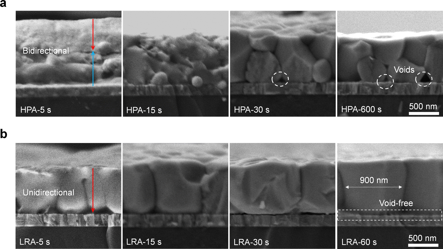 | ||
| Fig. 2 (a) Cross-sectional SEM images of Sn–Pb perovskite films under HPA for different annealing times ranging from 5 s to 600 s. (b) Cross-sectional SEM images of Sn–Pb perovskite films under LRA for different annealing times ranging from 5 s to 60 s. | ||
Then, we further investigated the morphology of the HPA and LRA films at the top surface and the bottom buried interface (Fig. S8, ESI†). Both the HPA and LRA films exhibited regular grains (Fig. 3b and e), but the LRA film has a smaller surface roughness of 29.9 nm, which is attributed to the stable temperature during the LRA process and the uniform heat distribution (Fig. 3a and d). For the HPA film, certain regions even exhibit depressions deeper than 100 nm. For the bottom interface, significant differences were observed (Fig. 3c and f). For the HPA film, rough morphology and numerous microvoids at the buried interface (more than 20 pcs per square micron) are visually observed. These characteristics are consistent with the effects of residual solvents.25 During the HPA process, the heating is slow and gradual, allowing the residual solvent to remain in the perovskite film for a longer time before evaporation. This prolonged residence time gives the solvent more time to interact with the perovskite, leading to erosion and dissolution. When the solvent molecules finally evaporate, they leave voids at the bottom buried interface. The imperfect buried contact between the perovskite and the charge transport layer could cause harmful defects and degrade the device performance. In contrast, the LRA film exhibits a smooth and void-free bottom interface, confirming the advantage of rapid solvent evaporation in removing the buried residual solvent (Fig. 3f). During the LRA process, the heating is rapid, significantly increasing the rate of solvent evaporation. The rapid evaporation minimizes the time and likelihood of solvent molecules interacting with the perovskite, thereby preventing erosion and dissolution. As a result, void formation is effectively suppressed. Additionally, the photons involved in the LRA process did not introduce additional oxidation of Sn2+ (Fig. S9, ESI†).
 | ||
| Fig. 3 (a) The top-view AFM image of the HPA perovskite film. (b) The top-view SEM image of the HPA perovskite film. (c) The bottom-view SEM image of the HPA perovskite film. (d) The top-view AFM image of the LRA perovskite film. (e) The top-view SEM image of the LRA perovskite film. (f) The bottom-view SEM image of the LRA perovskite film. | ||
Next, we begin to focus on the photoelectric properties of the HPA and LRA films. For the HPA film, the elemental distribution was reported to be uneven in profiling because the slow heating rate could amplify the inconsistent crystallization process of Sn-based and Pb-based perovskites (Fig. S10, ESI†).28,29 As shown in time of flight-secondary ion mass spectrometry (TOF-SIMS) images of Sn–Pb perovskites (Fig. 4a), Sn enrichment is observed at the upper surface, with 1.5 times higher than in the bulk. This surface compositional segregation of Sn–Pb perovskites caused a deviation from the optimal bandgap. The different photoluminescence (PL) emission positions at the front and back surfaces of the HPA films also confirmed this result (Fig. 4d). The PL emission position at the front surface shifts to a higher energy (blue shift), indicating a larger bandgap in the surface layer, which subsequently affects the overall device performance. In contrast, the heating rate of LRA is much faster, which can largely shorten the difference in growth time for both Sn-based and Pb-based perovskites. Therefore, the LRA film showed a more uniform Sn and Pb distribution (Fig. 4b). It can also be confirmed by the similar PL emission position at the front and back surfaces (Fig. 4e).
 | ||
| Fig. 4 (a) Elemental distribution for Sn–Pb perovskite films after the HPA process. (b) Elemental distribution for Sn–Pb perovskite films after the LRA process. (c) DLCP measurements for Sn–Pb perovskite films under different annealing conditions. (d) Steady-state PL spectra of the perovskite films at the front and back surfaces after the HPA process. (e) Steady-state PL spectra of the perovskite films at the front and back surfaces after the LRA process. (f) PLQYs of Sn–Pb perovskite films under different annealing conditions. (g) Spectro-temporal TA mapping of the perovskite film after the HPA process. (h) Spectro-temporal TA mapping of the perovskite film after the LRA process. (i) TRPL spectra of Sn–Pb perovskite films under different annealing conditions. | ||
Film stratification and voids at the bottom interface could increase detrimental defects. We thus compared the defect distribution in HPA and LRA Sn–Pb perovskite films using drive-level capacitance profiling (DLCP, Fig. 4c), and the structure diagram of the test device is shown in Fig. 5a. The defect density near the interface with C60 was similar for both films. However, the defect density near the interface with PEDO:PSS was lower in the LRA films, attributed to the void suppression at the bottom buried interface. Within the bulk of the film, the LRA film also exhibits a lower defect density, benefiting from a more uniform compositional distribution and the prevention of stratification. LRA films also exhibited a twice higher PL quantum yield (PLQY), indicating suppressed non-radiative recombination (Fig. 4f). Transient absorption (TA) spectroscopy was used to quantify the energy shift and photogenerated carrier lifetime in Sn–Pb perovskite films. After pump light emission, a pronounced bleach peak appeared at ∼1000 nm, and the bleach peak position moved with time. The HPA film showed a redshift of 15.9 meV, while the LRA film only shifted to 7.3 meV (Fig. 4g, h and S11, ESI†). The smaller energy shift indicates that bandgap fluctuation or band tail state in LRA films is suppressed. Time-resolved photoluminescence (TRPL) measurements revealed that the carrier lifetime of the LRA film (608 ns) is nearly triple that of the HPA film (206 ns, Fig. 4i and Table S3, ESI†).
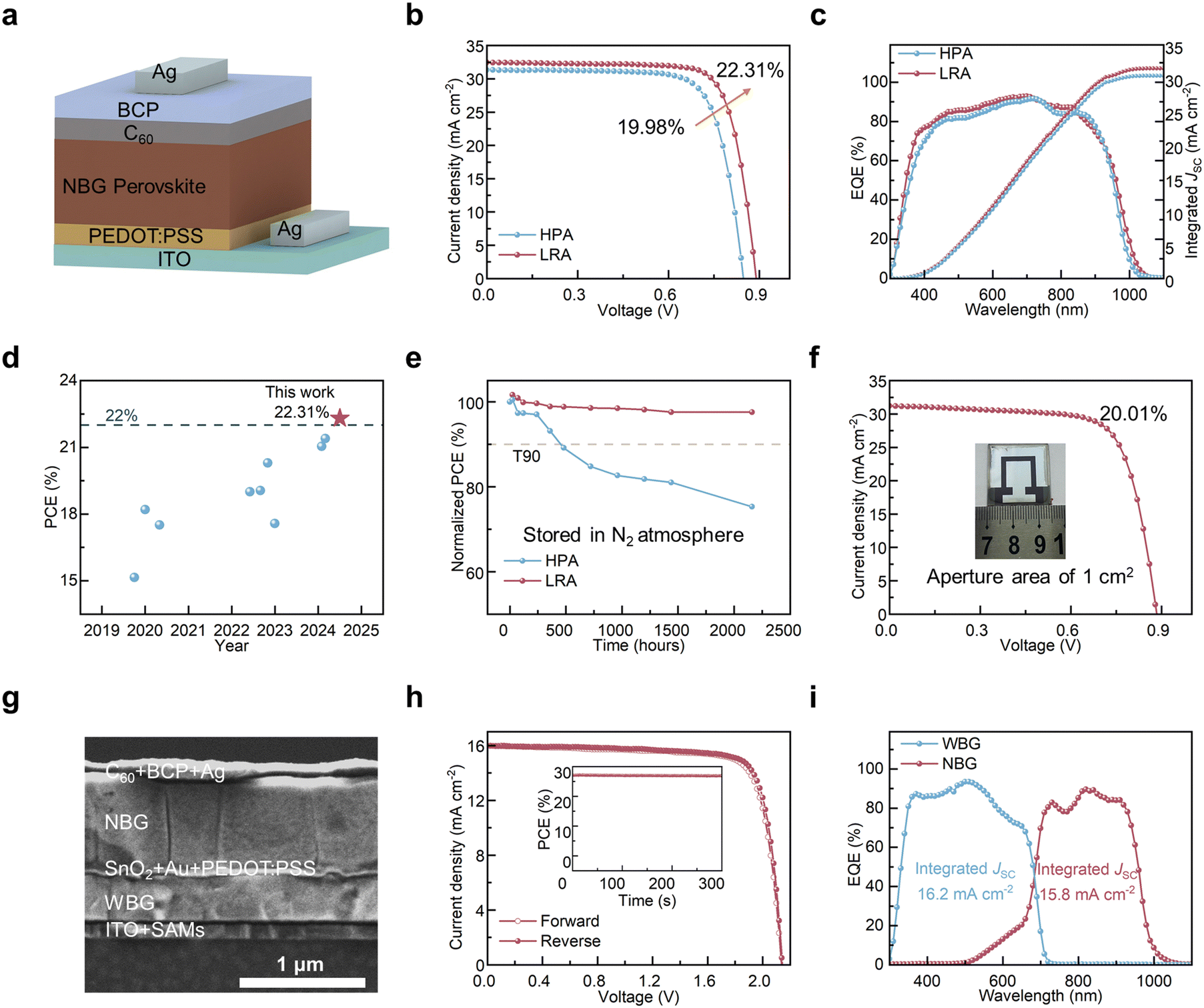 | ||
| Fig. 5 (a) A structure schematic diagram of Sn–Pb PSC. (b) J–V curves of Sn–Pb PSCs under AM 1.5G solar illumination. (c) EQE spectra of HPA and LRA devices. (d) Efficiency of antisolvent-free Sn–Pb mixed PSCs in the literature. (e) PCE of Sn–Pb mixed PSCs as a function of storage time. (f) J–V curves of 1-cm2 Sn–Pb PSCs. (g) The cross-sectional SEM image of all-perovskite tandem solar cells. (h) J–V curves of all-perovskite tandem solar cells. The insert is the stable power output. (i) EQE spectra of the bottom and top subcells. | ||
Using the vacuum-assisted technique, we fabricated Sn–Pb PSCs with the structure of ITO/PEDOT:PSS/NBG/C60/2,9-dimethyl-4,7-diphenyl-1,10-phenanthroline (BCP)/Ag (Fig. 5a). We compared the PSC performance under LRA times and chose 60 s as the optimal LRA duration (Fig. S12, ESI†). Compared to HPA devices with a VOC of 0.848 V and an efficiency of 19.98%, LRA devices achieved a higher VOC of 0.889 V and an improved efficiency of 22.31%, creating a record not only for the vacuum-assisted method but also for the antisolvent-free methods (Fig. 5b, d and Table S5, ESI†). Due to the reduced voids at the bottom buried interface, the LRA PSCs exhibit higher external quantum efficiency (EQE) in the short wavelength. The integrated short-circuit current density (JSC) values from the EQE spectra were 30.39 and 31.48 mA cm−2, respectively, in good agreement with the JSC determined from J–V measurements (Fig. 5c and Fig. S13, ESI†). The increase in JSC is not only due to the high-quality and thicker Sn–Pb perovskite films fabricated by the LRA process but also related to its efficient suppression of film stratification and buried interface voids. The improved VOC can be explained by the above-mentioned photoelectric characterization in Fig. 3. The suppressed charge–carrier recombination and improved charge transfer also offer a further explanation (Fig. S14, ESI†). Statistics of device efficiency confirmed the reproducibility of the efficiency improvement with LRA (Fig. S15, ESI†).
We further monitored the long-term storage stability of PSCs (Fig. 5e). Compared to HPA devices with an efficiency decay to below 90% of the initial value after 500 hours, LRA samples maintained over 95% of their initial efficiency even after more than 2000 hours in nitrogen without encapsulation. The thermal aging experiments also demonstrated that Sn–Pb PSCs fabricated using the LRA method exhibit superior thermal stability (Fig. S16, ESI†). This improvement in stability is attributed to the uniform elemental composition (or say less phase segregation) and the reduced defects. Additionally, based on the advantages of vacuum-assisted technology and LRA in large-area fabrication, we fabricated 1 cm2 Sn–Pb perovskite films and devices. Compared to the 1 cm2 HPA Sn–Pb PSCs (Fig. S17, ESI†), LRA-based devices showed better performance, achieving an efficiency exceeding 20% (Fig. 5f and Table 1), which is the highest efficiency achieved using an antisolvent-free method.
| Samples | Area (cm2) | V OC (V) | J SC (mA cm−2) | FF (%) | PCE (%) |
|---|---|---|---|---|---|
| HPA | 0.0448 | 0.848 | 31.34 | 75.22 | 19.98 |
| LRA | 0.0448 | 0.889 | 32.47 | 77.26 | 22.31 |
| 1 | 0.884 | 31.21 | 72.52 | 20.01 |
Based on the high-efficiency LRA devices and combined with the previously achieved high-efficiency wide-bandgap PSCs (Fig. S18 and S19, ESI†),30,31 we prepared all-perovskite tandem solar cells using an antisolvent-free method. The SEM cross-sectional image of the all-perovskite tandem structure is shown in Fig. 5g. Due to high-efficiency narrow-bandgap PSCs and wide-bandgap PSCs, the tandem solar cell fabricated by the LRA method achieved a VOC of 2.143 V, a JSC of 15.98 mA cm−2, an FF of 80.65%, and a PCE of 27.62% (Fig. 5h and Table S4, ESI†). Compared to HPA tandem solar cells (Fig. S20 and S21, ESI†), the efficiency of the all-perovskite tandem solar cell fabricated using the LRA method showed an improvement over 1.5%. This represents the top-level efficiency for all-perovskite tandem solar cells fabricated using the antisolvent-free method. We tested the stability using maximum power point (MPP) tracking in air and under simulated 1-sun illumination (Fig. S22, ESI†). An encapsulated LRA tandem retained 80% of its original PCE after more than 100 h continuous operation, surpassing the 19 h of the HPA device.
3. Conclusions
In conclusion, we developed an LRA method to achieve top-down unidirectional growth for vacuum-assisted Sn–Pb perovskite films. This innovative approach suppresses film stratification and void formation at the bottom buried interface, thereby reducing the defect density in the Sn–Pb perovskite films. We achieved a remarkable efficiency of 22.31% for Sn–Pb PSCs utilizing a vacuum-assisted method and a top-level efficiency of 27.62% for all-perovskite tandem solar cells. These outcomes signify significant efficiency breakthroughs for both narrow-bandgap single-junction and all-perovskite tandem solar cells. Our work not only offers valuable insights into the vacuum-assisted process for Sn–Pb PSCs but also presents a promising approach for developing high-efficiency devices using the vacuum-assisted method.4. Experimental section
Materials and solvents
The raw materials and solvents were not subjected to any purification. PbI2 (99.999%), SnI2 (99.999%), PbBr2 (99.99%), FAI (>99%), MAI (>99%), PEAI (99.5%) and NiO nanocrystals (99.999%) were purchased from Advanced Election Technology Co., Ltd. MACl (99.5%), Pb(SCN)2 (99.5%), FABr (99.5%), CsBr (99.9%), CsI (99.999%), PbCl2 (99.9%), DMAI (99.5%), EDAI2 (99.5%), PDADI (99.5%), PEDOT:PSS and C60 were purchased from Xi'an Yuri Solar Co., Ltd. SnF2 (99%), Sn powder (99.999%), N,N-dimethylformamide (DMF, 99.8%, anhydrous), dimethyl sulfoxide (DMSO, 99.9%, anhydrous), chlorobenzene (CB, 99.9%, anhydrous) and isopropanol (IPA, 99.5%, anhydrous) were purchased from Sigma-Aldrich. 4PADCB was purchased from Vizuchem Co., Ltd (Shanghai, China). Bathocuproine (BCP) was purchased from TCI. The glass ITO with a sheet resistance of 7–9 ohm sq−1 was purchased from Advanced Election Technology Co. Ltd.Narrow-bandgap Cs0.1FA0.6MA0.3Sn0.5Pb0.5I3 perovskite precursor preparation
The narrow-bandgap perovskite precursor with a concentration of 1.8 mol L−1 was prepared by mixing CsI (46.8 mg), FAI (185.7 mg), MAI (85.8 mg), SnI2 (335.3 mg), PbI2 (414.9 mg), SnF2 (14.1 mg) and Pb(SCN)2 (2.7 mg) in mixed solvents of 0.25 mL of DMSO and 0.75 mL of DMF. The precursor solution was filtered through a 0.22 μm PTFE filter before use.Wide-bandgap DMA0.1Cs0.5FA0.4PbI0.85Br0.15 perovskite precursor preparation
The wide-bandgap perovskite precursor with a concentration of 1 mol L−1 was prepared by mixing CsBr (42.56 mg), FABr (31.24 mg), DMAI (17.30 mg), MACl (3.38 mg), Pb(SCN)2 (3.25 mg), PbCl2 (13.90 mg), PEAI (2.5 mg), FAI (42.99 mg), CsI (51.99 mg), PbBr2 (55.05 mg), and PbI2 (391.85 mg) in mixed solvents of 0.2 mL of DMSO and 0.8 mL of DMF.32,33 The precursor solution was filtered through a 0.22 μm PTFE filter before use.Narrow-bandgap Cs0.1FA0.6MA0.3Sn0.5Pb0.5I3 PSC fabrication
The pre-patterned ITO/glass substrates were sequentially cleaned with a detergent, ultrapure water, isopropanol, and ethanol for 30 min each. PEDOT:PSS was spin-coated onto ITO substrates at 2000 rpm for 30 s and annealed at 100 °C for 10 min in air. After cooling, we transferred the substrates to a nitrogen glovebox to fabricate Sn–Pb mixed perovskite films. The Sn–Pb mixed perovskite films were spin-coated onto the substrates at 4000 rpm for 8 s. The wet perovskite films were directly transferred into a vacuum chamber (120 mL) for a pumping time of >15 s at a vacuum degree of ∼1 Pa. The perovskite films subjected to normal annealing were placed on a hot-plate at 100 °C for 10 min. In contrast, the perovskite films undergoing LRA were positioned beneath a 375 W tungsten filament lamp, illuminated for 1 min. The distance between the tungsten lamp and the surface was adjusted to maintain the surface of the film temperature at 100 °C. Before each experiment, we calibrated the distance between the light source and the sample, and we used a thermocouple to verify the temperature. After cooling, the perovskite films were post-treated by spinning a solution of EDAI2 (0.5 mg mL−1) in a 1![[thin space (1/6-em)]](https://www.rsc.org/images/entities/char_2009.gif) :1 IPA:CB solvent at 4000 rpm. for 30 s, followed by heating at 100 °C for 5 min. Finally, C60 (15 nm)/BCP (7 nm)/Ag (150 nm) were sequentially deposited on top of the perovskite by thermal evaporation.
:1 IPA:CB solvent at 4000 rpm. for 30 s, followed by heating at 100 °C for 5 min. Finally, C60 (15 nm)/BCP (7 nm)/Ag (150 nm) were sequentially deposited on top of the perovskite by thermal evaporation.
All-perovskite tandem solar cell fabrication
NiOx nanocrystals dissolved in deionized water (3 mg mL−1) was spin-coated onto the ITO substrates at 4500 rpm for 30 s, followed by a hot-plate annealing process at 150 °C for 10 min. After cooling, oxygen plasma was used to treat the substrate for 5 min, and then the self-assembled monolayer 4PADCB dissolved in ethanol (0.5 mg mL−1) was spin-coated onto the substrates at 3000 rpm for 30 s, followed by heating at 100 °C for 10 min. After cooling, 50 μL of the wide-bandgap perovskite precursor was dropped on the substrate and spin-coated through a two-step process: 1000 rpm for 5 s and 4000 rpm for 40 s. At the twentieth second, hot gas flow (70 m s−1, 50 °C) started and the gas flow was maintained for 5 s. After gas-assisted spin coating, the samples were then annealed at 100 °C for 10 min. After cooling, the wide-bandgap perovskite films were post-treated by spinning PDAI2 solution (1 mg mL−1 in 1:1 IPA:toluene) at 5000 rpm for 30 s, followed by heating at 80 °C for 5 min. Then, 15 nm C60 was deposited on top of the wide-bandgap perovskite films by thermal evaporation. The samples were then transferred to an ALD system to deposit 30 nm SnO2. After this, a 1 nm layer of Au was thermally evaporated onto the film. Subsequently, narrow-bandgap subcells were fabricated using the above-mentioned methods.
Device characterization
The GIXRD pattern was tested using an X pert pro MRD system (Philips, Netherlands), with Cu Ka radiation and an anode operating at 40 kV and 250 mA. Perovskite film morphology was imaged with a scanning electron microscope (SEM, FEI Navo NanoSEM450). The AFM images were obtained in the ambient atmosphere using a Bruker Dimension Icon XR AFM. The time of flight-secondary ion mass spectrometry (TOF-SIMS) measurement (Helios 5 HX/Helios 5 UX/Helios 5 FX DualBeam) was performed with a BiMn primary ion beam (3-lens 30 keV) for the analysis. The steady-state PL was measured using a laser confocal Raman spectrometer (LabRAM HR800, Horiba JobinYvon) and the light was illuminated from both the front and back surfaces of the perovskite films (excited by 532 nm). The PLQY was measured using an Edinburgh FLS-1000 spectrometer. The TRPL was performed using a spectrofluorometer (QuantaMaster 8000 series fluorometers, Horiba), and the samples were excited using a 532 nm pulsed laser. The DLCP test used an Agilent E4294A impedance analyzer. The scanning voltage offset range was −0.1 V to 0.7 V and the a.c. voltage frequency was set to 10 kHz. The femtosecond TA measurements were performed on a Helios spectrometer (Ultrafast Systems) pumped using a Ti:sapphire regenerative amplifier (Legend Elite, Coherent) operating at 5 kHz with a fundamental wavelength of 800 nm and a pulse width of ∼40 fs. The excitation pulses were tuned in frequency using an optical parametric amplifier (light conversion). The current density–voltage (J–V) characteristics and steady-state output of all the solar cells were measured under 100 mW cm−2 light illumination (AM 1.5G) using a Newport Oriel 92192 solar simulator and a digital source meter (Keithley 2400) in a nitrogen glovebox. EQE measurements were performed in ambient air using a QE system (EnliTech) with monochromatic light focused on a device pixel and a chopper frequency of 20 Hz. For EQE measurements of tandem solar cells, two light-emitting diodes with emission wavelengths at 450nm and 850nm were used as the bias lights to measure NBG and WBG subcells, respectively. The annealing model employs the electromagnetic waves, frequency domain physics interface from the wave optics module in COMSOL Multiphysics software. In solid heat transfer modules, the sides of the model are set under periodic boundary conditions, while the top surface is subjected to natural convection cooling under room temperature conditions. For the thermal annealing model, the substrate is set to 100 °C, while for the LRA model, the substrate is set to room temperature, 20 °C. The model then calculates the transient temperature distribution within the device over time.
Author contributions
J. T. and C. C. conceived the idea and directed the overall project. C. G. fabricated the devices and conducted the characterization studies. Q. X. participated in the device fabrication and results and discussion. D. L. assisted to optimize the wide-bandgap PSCs. W. Y. provided the COMSOL modeling and simulations. Y. Z. contributed to the data analysis. P. Z. assisted with the DLCP testing and analysis. J. Y., G. L., L. X., Y. Z. and H. S. participated in optimizing the manuscript. C. G. and C. C. wrote the manuscript, and all authors discussed the results and commented on the paper.Data availability
The data that support the findings of this study are available from the corresponding author upon reasonable request.Conflicts of interest
The authors declare no competing interests.Acknowledgements
This work was supported by the National Natural Science Foundation of China (62174064 and 52330004), the Guangdong Provincial Key Laboratory of Manufacturing Equipment Digitization (2023B1212060012), the Fundamental Research Funds for the Central Universities (2021XXJS028), and the Innovation Project of Optics Valley Laboratory (OVL2021BG008 and OVL2023ZD002). We also appreciate the TA test support from Prof. Wenxi Liang at the Huazhong University of Science and Technology and the COMSOL simulation from Prof. Changlei Wang at Soochow University. The authors appreciate the Open and Shared Service Platform for Large Instruments and Equipment of School of Optical and Electronic Information of the Huazhong University of Science and Technology (HUST) for offering SEM measurements. We thank the Optoelectronic Micro & Nano Fabrication and Characterizing Facility, Wuhan National Laboratory for Optoelectronics of the Huazhong University of Science and Technology, and the Analytical and Testing Center of HUST for their support. The computation is completed in the HPC Platform of the Huazhong University of Science and Technology.References
- F. Yang and K. Zhu, Adv. Mater., 2024, 2314341 CrossRef CAS
.
- T. Leijtens, K. A. Bush, R. Prasanna and M. D. McGehee, Nat. Energy, 2018, 3, 828 CrossRef CAS
- K. Alberi, J. J. Berry, J. J. Cordell, D. J. Friedman, J. F. Geisz, A. R. Kirmani, B. W. Larson, W. E. McMahon, L. M. Mansfield, P. F. Ndione, M. Owen-Bellini, A. F. Palmstrom, M. O. Reese, S. B. Reese, M. A. Steiner, A. C. Tamboli, S. Theingi and E. L. Warren, Joule, 2024, 8, 685 CrossRef
- W. Tang, T. Liu, M. Zhang, F. Yuan, K. Zhou, R. Lai, Y. Lian, S. Xing, W. Xiong, M. Zhang, F. Gao, B. Zhao and D. Di, Matter, 2023, 6, 3782 CrossRef CAS
- Z. Li, T. R. Klein, D. H. Kim, M. Yang, J. J. Berry, M. F. A. M. Van Hest and K. Zhu, Nat. Rev. Mater., 2018, 3, 18017 CrossRef CAS
- S. Ghosh, S. Mishra and T. Singh, Adv. Mater. Interfaces, 2020, 7, 2000950 CrossRef CAS
- A. Ng, Z. Ren, H. Hu, P. W. K. Fong, Q. Shen, S. H. Cheung, P. Qin, J. Lee, A. B. Djurišić, S. K. So, G. Li, Y. Yang and C. Surya, Adv. Mater., 2018, 30, 1804402 CrossRef
- C. Ge, B. Jiang, J. Zhu, P. Zhang, R. Ma, S. Yan, Z. Liu, A. Shaker, M. S. Salem, J. Luo, L. Xu, J. Yang, Z. Li, H. Song, C. Chen and J. Tang, Adv. Funct. Mater., 2024, 2400075 CrossRef CAS
- J. Zhong, W. Wu, L. Ding and D. Kuang, Energy Environ. Mater., 2021, 4, 277 CrossRef CAS
- L. Zeng, S. Chen, K. Forberich, C. J. Brabec, Y. Mai and F. Guo, Energy Environ. Sci., 2020, 13, 4666 RSC
- X. Li, D. Bi, C. Yi, J.-D. Décoppet, J. Luo, S. M. Zakeeruddin, A. Hagfeldt and M. Grätzel, Science, 2016, 353, 58 CrossRef CAS
- X. Zhao, Z. Zhang, Y. Zhu, F. Meng, M. Li, C. Wang, W. Gao, Y. Feng, R. Li, D. He, J. Chen and C. Chen, Nano Lett., 2023, 23, 11184 CrossRef CAS
- J. Su, X. Zheng, H. Guo, S. Jiang, H. Tian, J. Yang, X. Ye, H. Cai, J. Ni, J. Qiu and J. Zhang, J. Electron. Mater., 2022, 51, 2396 CrossRef CAS
- K. Xiao, R. Lin, Q. Han, Y. Hou, Z. Qin, H. T. Nguyen, J. Wen, M. Wei, V. Yeddu, M. I. Saidaminov, Y. Gao, X. Luo, Y. Wang, H. Gao, C. Zhang, J. Xu, J. Zhu, E. H. Sargent and H. Tan, Nat. Energy, 2020, 5, 870 CrossRef CAS
- C. Li, Z. Song, C. Chen, C. Xiao, B. Subedi, S. P. Harvey, N. Shrestha, K. K. Subedi, L. Chen, D. Liu, Y. Li, Y.-W. Kim, C. Jiang, M. J. Heben, D. Zhao, R. J. Ellingson, N. J. Podraza, M. Al-Jassim and Y. Yan, Nat. Energy, 2020, 5, 768 CrossRef CAS
- S. Hu, J. Thiesbrummel, J. Pascual, M. Stolterfoht, A. Wakamiya and H. J. Snaith, Chem. Rev., 2024, 124, 4079 CrossRef CAS
- B. Abdollahi Nejand, I. M. Hossain, M. Jakoby, S. Moghadamzadeh, T. Abzieher, S. Gharibzadeh, J. A. Schwenzer, P. Nazari, F. Schackmar, D. Hauschild, L. Weinhardt, U. Lemmer, B. S. Richards, I. A. Howard and U. W. Paetzold, Adv. Energy Mater., 2020, 10, 1902583 CrossRef CAS
- H. Lai, J. Hu, X. Zhou, L. Cai, Q. He, C. Chen, Z. Xu, X. Xiao, D. Lan, Y. Mai and F. Guo, Sol. RRL, 2022, 6, 2200619 CrossRef CAS
- B. Abdollahi Nejand, D. B. Ritzer, H. Hu, F. Schackmar, S. Moghadamzadeh, T. Feeney, R. Singh, F. Laufer, R. Schmager, R. Azmi, M. Kaiser, T. Abzieher, S. Gharibzadeh, E. Ahlswede, U. Lemmer, B. S. Richards and U. W. Paetzold, Nat. Energy, 2022, 7, 620 CrossRef CAS
- X. Zhou, H. Lai, T. Huang, C. Chen, Z. Xu, Y. Yang, S. Wu, X. Xiao, L. Chen, C. J. Brabec, Y. Mai and F. Guo, ACS Energy Lett., 2023, 8, 502 CrossRef CAS
- L. Zeng, Z. Chen, S. Qiu, J. Hu, C. Li, X. Liu, G. Liang, C. J. Brabec, Y. Mai and F. Guo, Nano Energy, 2019, 66, 104099 CrossRef CAS
- R. Lin, Y. Wang, Q. Lu, B. Tang, J. Li, H. Gao, Y. Gao, H. Li, C. Ding, J. Wen, P. Wu, C. Liu, S. Zhao, K. Xiao, Z. Liu, C. Ma, Y. Deng, L. Li, F. Fan and H. Tan, Nature, 2023, 620, 994 CrossRef CAS PubMed
- A. D. Taylor, Q. Sun, K. P. Goetz, Q. An, T. Schramm, Y. Hofstetter, M. Litterst, F. Paulus and Y. Vaynzof, Nat. Commun., 2021, 12, 1878 CrossRef CAS
- S. L. Hamukwaya, H. Hao, Z. Zhao, J. Dong, T. Zhong, J. Xing, L. Hao and M. M. Mashingaidze, Coatings, 2022, 12, 252 CrossRef CAS
- M. Wang, C. Fei, M. A. Uddin and J. Huang, Sci. Adv., 2022, 8, 5977 CrossRef
- T. Ma, Y. An, Z. Yang, Z. Ai, Y. Zhang, C. Wang and X. Li, Adv. Funct. Mater., 2023, 33, 2212596 CrossRef CAS
- D. Wang, C. Wu, W. Luo, X. Guo, X. Qi, Y. Zhang, Z. Zhang, N. Zhu, B. Qu, L. Xiao and Z. Chen, ACS Appl. Mater. Interfaces, 2019, 11, 20943 CrossRef CAS
- J. Cao, H. Loi, Y. Xu, X. Guo, N. Wang, C. Liu, T. Wang, H. Cheng, Y. Zhu, M. G. Li, W. Wong and F. Yan, Adv. Mater., 2022, 34, 2107729 CrossRef CAS PubMed
- H. Loi, J. Cao, C. Liu, Y. Xu, M. G. Li and F. Yan, Small, 2023, 19, 2205976 CrossRef CAS
- Q. Xiao, A. Zhang, W. Ye, X. Yang, Y. Zhu, B. Jiang, C. Ge, X. Li, H. Song, C. Chen and J. Tang, Sol. RRL, 2023, 7, 2300486 CrossRef CAS
- A. Zhang, M. Li, C. Dong, W. Ye, Y. Zhu, J. Yang, L. Hu, X. Li, L. Xu, Y. Zhou, H. Song, C. Chen and J. Tang, Chem. Eng. J., 2024, 494, 153253 CrossRef CAS
- A. F. Palmstrom, G. E. Eperon, T. Leijtens, R. Prasanna, S. N. Habisreutinger, W. Nemeth, E. A. Gaulding, S. P. Dunfield, M. Reese, S. Nanayakkara, T. Moot, J. Werner, J. Liu, B. To, S. T. Christensen, M. D. McGehee, M. F. A. M. Van Hest, J. M. Luther, J. J. Berry and D. T. Moore, Joule, 2019, 3, 2193 CrossRef CAS
- J. Wen, Y. Zhao, Z. Liu, H. Gao, R. Lin, S. Wan, C. Ji, K. Xiao, Y. Gao, Y. Tian, J. Xie, C. J. Brabec and H. Tan, Adv. Mater., 2022, 34, 2110356 CrossRef CAS PubMed
Footnote |
| † Electronic supplementary information (ESI) available. See DOI: https://doi.org/10.1039/d4ee03419h |
| This journal is © The Royal Society of Chemistry 2025 |