
 Open Access Article
 This Open Access Article is licensed under a
 Creative Commons Attribution 3.0 Unported Licence
High coordination-solvent bathing for efficient crystallization of MA-free triple halide perovskite solar cells†
José J.
Jerónimo-Rendon
 a,
Somayeh
Gholipour
*ab,
Sofya
Svetlosanova
a,
Rajarshi
Roy
a,
Stephan
Boehringer
a,
Seyma
Topcu
a,
Weiwei
Zuo
a,
Mohammadreza
Zohdi
a,
Mojtaba
Ataei
a,
Mayank
Kedia
ab,
Anna
Zhuravlova
c,
Silver-Hamill
Turren-Cruz
de,
Paolo
Samorì
c,
Antonio Gaetano
Ricciardulli
c,
Mahdi
Malekshahi Byranvand
*ab and
Michael
Saliba
*ab
a,
Somayeh
Gholipour
*ab,
Sofya
Svetlosanova
a,
Rajarshi
Roy
a,
Stephan
Boehringer
a,
Seyma
Topcu
a,
Weiwei
Zuo
a,
Mohammadreza
Zohdi
a,
Mojtaba
Ataei
a,
Mayank
Kedia
ab,
Anna
Zhuravlova
c,
Silver-Hamill
Turren-Cruz
de,
Paolo
Samorì
c,
Antonio Gaetano
Ricciardulli
c,
Mahdi
Malekshahi Byranvand
*ab and
Michael
Saliba
*ab
aInstitute for Photovoltaics (ipv), University of Stuttgart, Stuttgart, 70569, Germany. E-mail: somayeh.gholipour@ipv.uni-stuttgart.de; mahdi.malekshahi@ipv.uni-stuttgart.de; michael.saliba@ipv.uni-stuttgart.de
bHelmholtz Young Investigator Group FRONTRUNNER, IEK5-Photovoltaik, Forschungszentrum Jülich, Jülich, 52425, Germany
cUniversité de Strasbourg, CNRS, ISIS UMR 7006, 8 allée Gaspard Monge, Strasbourg, 67000, France
dDepartment of Physical Chemistry, Polish Academy of Sciences, Warsaw, 01-224, Poland
eInstituto de Ciencia de los Materiales (ICMUV), Universitat de Valencia, Paterna, 46980, Spain
First published on 21st January 2025
Abstract
Many high-performance perovskite solar cells (PSCs) rely heavily on halogenated antisolvent methods, hampering their potential commercialization. In this work, the industry-compatible dimethyl sulfide (DMS) solvent, which coordinates strongly with the metal cation, is used in a bathing approach to investigate the crystallization of triple halide perovskites. The resulting thin films are more uniform exhibiting preferential crystal growth in the (001) direction (perpendicular to the substrate) and large grains of 444 ± 122 nm compared to 421 ± 147 nm for the reference films. Moreover, the electron diffusion length and lifetimes are enhanced from 1 to 3 μm and from 551 to 1050 ns, respectively, compared to the reference film. The champion solar cell based on our approach exhibits a power conversion efficiency (PCE) of 20.6%, comparable to the conventional lab-scale counterpart at 21.4%. Additionally, the long-term stability of our devices shows that 88% (similar to the reference at 93%) of the initial performance is retained after 60 days at room temperature with 60% relative humidity.
Broader contextImprovement of the limiting factors including scalable and high-quality film deposition is crucial for the commercial application of perovskite solar cells. Here, the antisolvent bathing (ASB) method with the high coordination dimethyl sulfide solvent has been explored as a promising candidates due to the efficient extraction of the precursor solvents lingering in the perovskite film. Using the ASB approach and 5 min annealing at 80 °C, highly crystalline films with an average grain size of 444 nm are observed. Furthermore, a photovoltaic performance at 20.6% is achieved together with a stability of 88% of the initial PCE, even after 60 hours of aging under ambient environmental conditions such as room temperature, and 60% relative humidity. |
1. Introduction
Metal-halide perovskite materials have attracted much attention in optoelectronics,1–4 due to their excellent absorption,5 long-range carrier diffusion lengths,6,7 low exciton binding energies,8 solution processability,9 optical tunability,10–12 low trap-state densities,13,14 and high defect tolerance.15,16 Such unique characteristics have resulted in perovskite solar cells (PSCs) with power conversion efficiencies (PCE) of >26% (single-junction)17 and >33.0% (perovskite/silicon tandem),18 respectively.To further develop large-scale, efficient, and stable photovoltaic (PV) panels, the realization of high-quality films featuring improved crystallinity and reduced trap state densities as well as tailored bandgap for target applications, is highly sought after.19 For example, triple halide perovskites with a bandgap from 1.6 to 1.7 eV have attracted interest for indoor or tandem PV10,19–22 as they offer high open-circuit voltage (VOC) due to reduced thermalization losses.23
Dripping an antisolvent, e.g. chlorobenzene (CB),24,25 ethyl ether,26 or toluene,27 onto an oversaturated perovskite precursor film, is a standard technique used to trigger crystallization.28 Nevertheless, despite the formation of high-quality films, many drawbacks arise, such as lack of scalability and reproducibility, and antisolvent toxicity.
To tackle these challenges, the industrially attractive scalable antisolvent bathing (ASB) method with diethyl ether (DE) was demonstrated by Zhou et al.,29 which delivered MAPbI3 perovskite films with >1 μm grains under adjusted cation/halide ratios and optimized annealing conditions at 80 °C for a longer time scale of 120 min, as well as solar cells exhibiting PCEs as high as 15.2%.30 Moderate PCEs were realized by further refinement, e.g. a dual ASB with ethyl acetate and DE (18% PCE),31 or a cold antisolvent bath at 0 °C (20% PCE).32 These reports demonstrate that upon changing the chemistry of solution and solvents, as well as adjusting the annealing procedure, it is possible to efficiently remove lingering PbI2, and δ-phase.33,34 Thus, optimization of the perovskite solution precursors with the ASB technique is desirable as it is industry-compatible with roll-to-roll processing of flexible substrates.28
Recently, we investigated dimethyl sulfide (DMS) as an industry-compatible coordinating solvent.35 DMS leads to the efficient extraction of DMSO in the MAI-PbI2-DMSO adduct at the intermediate phase by strong coordination between the sulfur-containing functional group of the DMS and the Pb2+ cations. In addition, due to the high vapor pressure and high Gutmann donor number of DMS, 53.7 kPa and 40.0 kcal mol−1 at 20 °C, respectively (compared to CB with 1.17 kPa, and 3.3 kcal mol−1, at 20 °C), the intermediate phase can be formed in a relatively short time during the annealing,35 resulting in a uniform nucleation and enabling controlled crystallization.
Here, using the ASB method with the DMS as coordination solvent, an optimized composition of mixed cation–anion triple halide perovskite i.e., Cs0.2FA0.8Pb((I0.82Br0.18)0.97Cl0.03)3, abbreviated as 3-hal, at different annealing temperatures (AT) with a short time scale of 5 min is studied. The optimized annealing temperature in the ASB method assists the larger electron diffusion length, carrier mobility, and lifetime in the perovskite films, as the crystal growth in the preferred orientation minimizes the spatial heterogeneity in their electronic properties.36 Therefore, the efficiency of the target n-i-p planar PSCs reached 20.6%, which is on par with the reference devices at 21.4%.
2. Results and discussion
The fabrication procedure of the perovskite films by the ASB method is illustrated in Fig. 1. The substrate preparation with the compact SnO2 electron-transport layer (ETL) deposition (step 1) is given in the Experimental section. As shown in step 2, the semi-transparent perovskite precursor solution is spin-coated on the ITO/SnO2 substrates. The as-coated wet films are immediately submerged in the DMS solvent for 2 min (step 3). As the precursor solvent is exposed to DMS, the color of the wet films gradually changes from green to dark brown (see Fig. 1, S1, and Video S1†).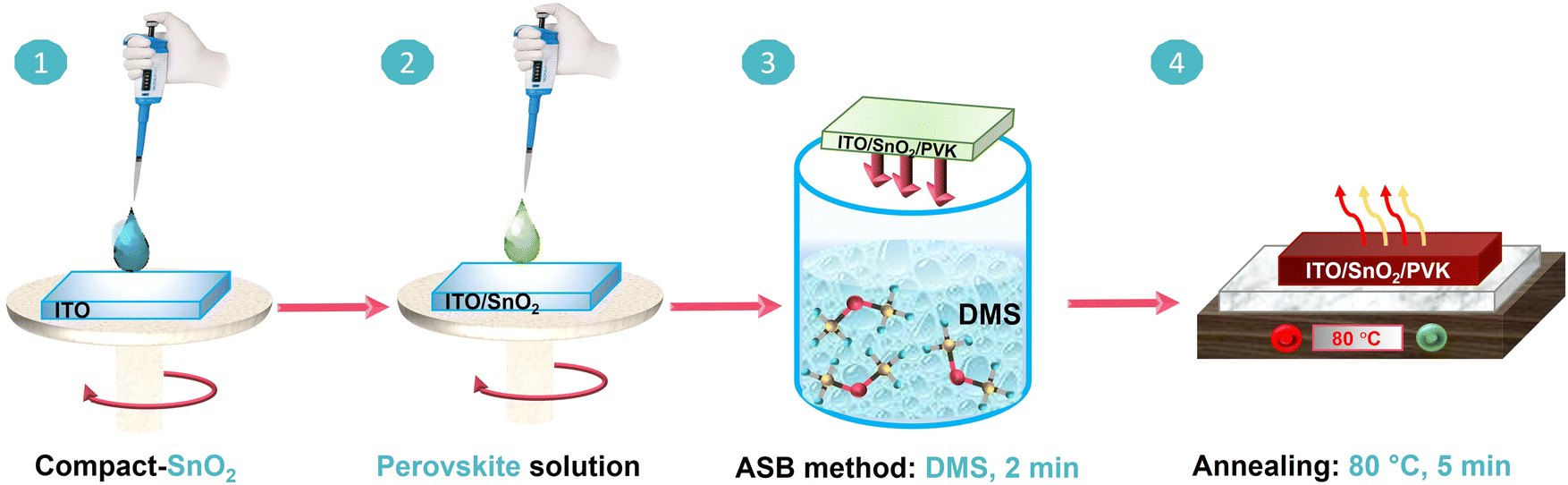 | ||
| Fig. 1 Sequential schematic of perovskite film fabrication using an ASB approach, Step 1: deposition of compact SnO2 layer on ITO coated glass substrate, step 2: spin coating of mixed cation–anion perovskite solution on ITO/SnO2, step 3: submerging the substrate in the DMS bath as antisolvent for 2 min, step 4: crystallization of perovskite film by annealing at optimized temperature of 80 °C, for 5 min. | ||
The films were then placed on a preheated hot plate at different annealing temperatures, i.e., 25 °C (AT25), 40 °C (AT40), 60 °C (AT60), 80 °C (AT80), and 100 °C (AT100) for 5 min (step 4). After annealing at the optimized temperature of 80 °C, relatively dark, nearly black, 3-hal films are observed. It is worth noting that due to the DMS miscibility with organic solvents,37 the precursor solvent can be extracted from the wet perovskite film via inward diffusion, followed by the supersaturation of the (wet) perovskite precursor film. Therefore, the efficient extraction of the precursor solvents highly depends on the solvent selection, which controls the nucleation and growth direction of the perovskite crystals.
To gain insights into the annealing temperature on the absorbance and bandgap energies, UV-vis, steady-state photoluminescence (PL), and time-resolved photoluminescence (TRPL) have been carried out on ITO/perovskite films. As shown in Fig. 2a, b, S2a, and Table S1,† with the increase in annealing temperature from 25 to 100 °C, the absorbance onset shifts to the shorter wavelengths and hence larger bandgap energies, whereas a shift to ∼756 nm (1.64 eV) is observed upon annealing at 80 °C. Similarly, blue shifts occur in steady-state PL (see Fig. 2c and S2a†), where the fabricated perovskite films by ASB and annealed at 80 °C exhibited clear PL emission at nearly 743 nm (1.67 eV) close to the reference films. It is worth mentioning that the PL and UV-vis spectra are shifting to the lower wavelength with increased annealing temperature to 80 °C, consistent with the halide inclusion into the unit cell of the 3D perovskite material.38 The two main factors affecting the bandgap value include unit cell volume associated with the strength of the Pb-halide bonding and octahedral tilting of the [Pb(I0.82Br0.18)64−] inorganic framework.39,40 Therefore, increasing the annealing temperature to 80 °C, the antibonding Pb and halogen orbitals are changing, causing a bandgap blueshift. Moreover, the TRPL analysis accompanied by extracted average lifetimes from fitting a double-exponential decay function implies the enhancement of the charge-carrier dynamics correlated with the perovskite film fabrication by the ASB method (see Fig. 2d and S2b†). As expected, the AT80 film exhibited a superior lifetime (∼1050 ns) compared to the reference sample (∼551 ns) (see Table S2†). In addition, the lifetime is enhanced from 218 to 994 ns, upon temperature increase from 25 to 60 °C. In contrast, the lifetime of the AT100 films is decreased to 319 ns. Therefore, the AT80 perovskite film shows a significantly prolonged recombination time of the generated carriers, enabling a longer diffusion length of charge carriers.
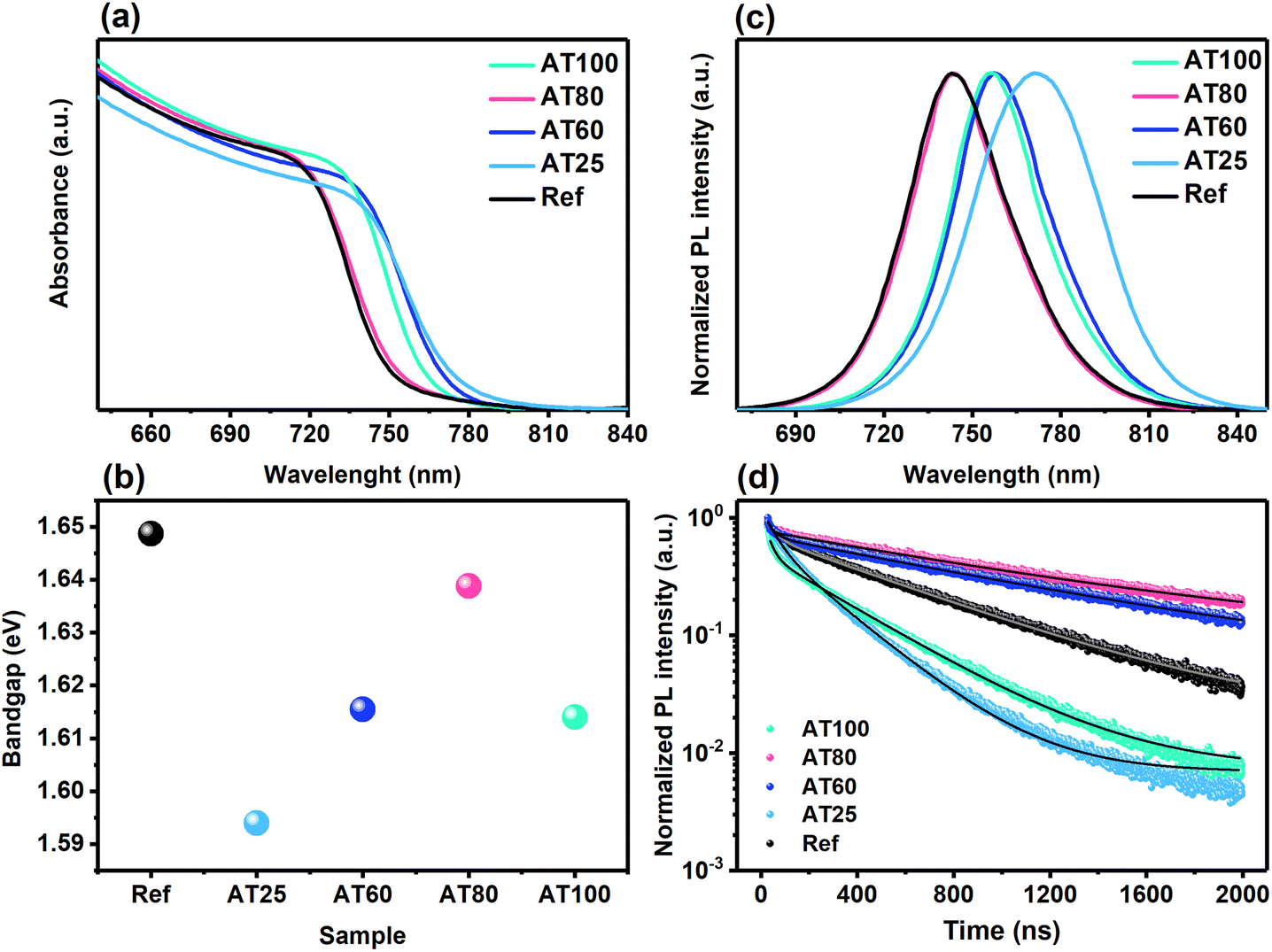 | ||
| Fig. 2 (a) UV-vis, (b) bandgap energies derived from absorbance spectra, (c) steady-state photoluminescence (PL), and (d) time-resolved photoluminescence (TRPL) spectra for perovskite films annealed at different temperatures, which was fabricated by using DMS as high coordination solvent in the ASB approach. | ||
The effect of the annealing temperature in the ASB method on the perovskite film crystallinity was studied via X-ray diffraction (XRD) patterns. As shown in Fig. S3,† all of the samples based on the ASB method exhibited the perovskite main peaks at 14.1° (001), 28.4° (002), and 31.9° (022), which match well with the corresponding reference perovskite deposited by dripped antisolvent (methyl acetate) method.41 As we observed in the magnified XRD patterns shown in Fig. 3a and S4,† the reference thin films exhibit higher intensity for the diffraction peaks, compared to the ASB ones. In addition, due to the stress developed during the ASB approach, 3-hal film main peaks shift to larger diffraction angles compared to the reference thin film, where the ITO peaks (see Fig. S3†) are detected at the same angle for both approaches. The area ratio of the main perovskite peak at 14.1° (001) to the PbI2 peak at 12.6° for the AT25, AT40, AT60, AT80, AT100 and reference thin films are calculated and shown in Fig. 3b. Therefore, by visualizing the main peak intensity at 14.1° (001) of the ASB-produced layers, the AT80 films have the highest peak area ratio compared to AT25, AT40, AT60 and AT100. In addition, the calculated area ratio of (001) to (011) and (001) to (111) diffraction peaks for AT80 films are larger than the reference, as shown in Fig. S5b and d,† respectively. This is consistent with the better crystallinity of AT80 with oriented crystals in the (001) direction perpendicular to the substrate. Moreover, the AT25 and AT40 films showed the photo-inactive δ-phase at 9°, which is suppressed significantly by increasing the temperature to 100 °C (see Fig. S3†). The XRD spectra shown in Fig. 3a, are related to the grazing incidence XRD (1-degree angle), which can penetrate to the bulk (30–50 nm from the surface). Therefore, the PbI2 still exists in the bulk of perovskite for annealing temperatures lower than 80 °C, and the halide cannot be included in the 3D perovskite at low annealing temperatures. Fig. S6a and b† show the full and magnified XRD patterns from the surface of the reference and ASB-produced layers annealed at different temperatures. As can be seen in Fig. S6c,† the calculated area ratio of the main perovskite peak at 14.1° (001) to the PbI2 peak at 12.6° for the reference and AT80 thin films have the lowest values compared to the AT25, AT40, AT60, and AT100. Moreover, the AT80 and AT100 have the same (001) to the PbI2 value, which shows that complete crystallization starts from 80 °C and will be the same at 100 °C.
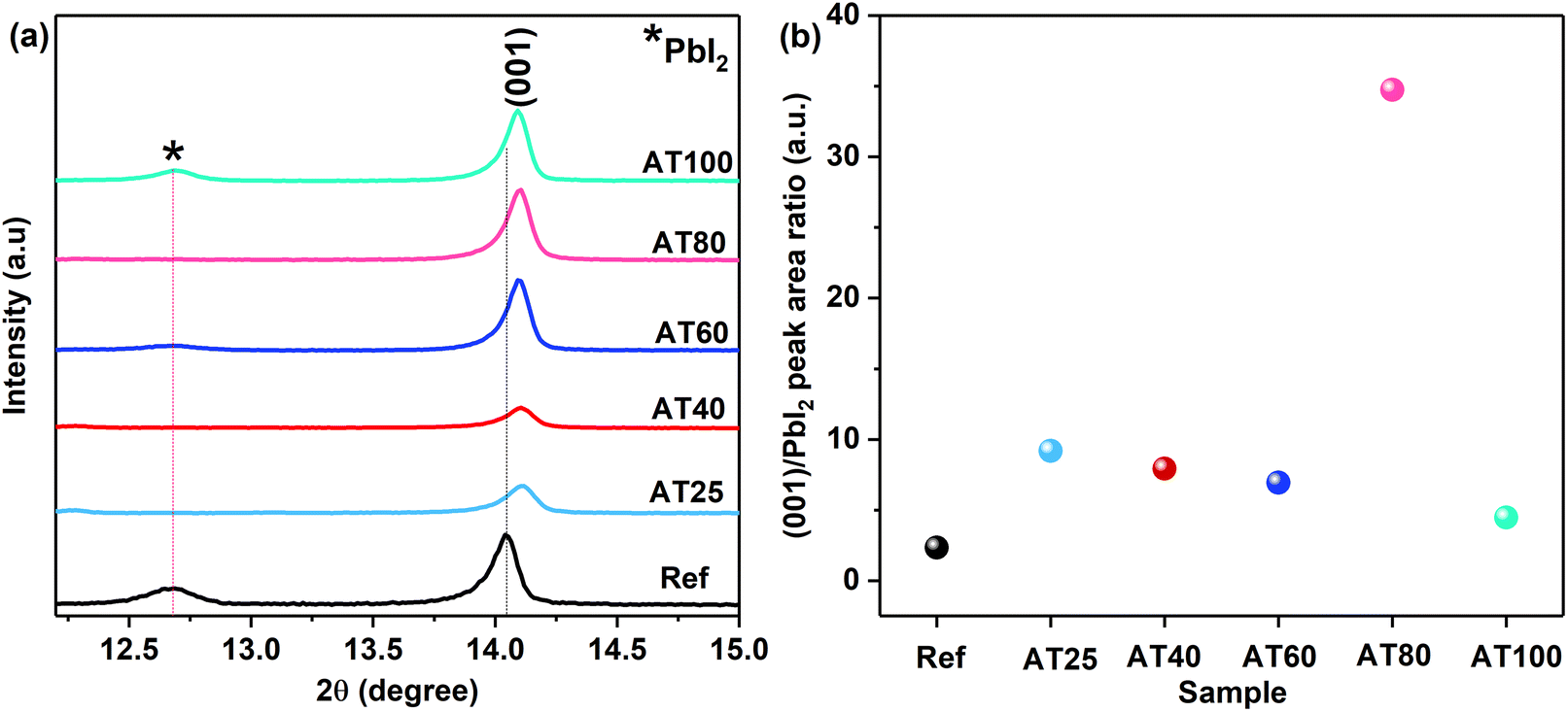 | ||
| Fig. 3 (a) The magnified XRD pattern for reference sample and 3-hal perovskite films grown on ITO/compact-SnO2 substrates with different annealing temperatures, and (b) (001) to PbI2 peak area ratio at different annealing temperatures. | ||
The top SEM image of each perovskite film was obtained to evaluate the impact of annealing temperature on the film morphology (Fig. 4a–f). By image analysis, the average grain sizes were determined to be 236 ± 77, 274 ± 74, 305 ± 110, 444 ± 122, and 304 ± 100 nm for the AT25, AT40, AT60, AT80 and AT100 perovskite films, respectively (see Fig. S7† for the grain size distribution). The increase in average grain size with increasing annealing temperature can be attributed to the reduced nuclei formation and grain boundaries during optimized temperature. However, upon annealing at 100 °C, the nucleation is much faster than the growth. Thus, the grain boundaries and the metallic lead defects are increased accordingly. In the case of the reference film, smaller grain sizes (421 ± 147 nm) with bright PbI2 crystals at grain boundaries can be seen in Fig. 4a. The brighter sites at the grain boundaries represent PbI2 impurities as verified by energy dispersive X-ray (EDX) analysis (see Fig. S8†), where the average electron density of PbI2 is higher than the perovskite crystals.42 These results are compatible with the XRD (surface) findings on the enhanced (001)/PbI2 peak area ratio for the films fabricated by the ASB approach (see Fig. S6c†). In addition, as shown in atomic force microscopy (AFM) images (see Fig. S9†), by increasing the annealing temperature from 25 to 80 °C, the surface roughness is reduced, as quantified by the root mean square roughness (RRMS) which decreased from 54.6 to 29.7 nm, respectively. It is worth mentioning that the perovskite film RRMS (29.7 nm) for the optimized annealing temperature (80 °C) of the ASB method is lower than that of the reference film (35.4 nm), which can lead to more uniform HTM film coverage, inducing reduced leakage currents and non-radiative loses.43
 | ||
| Fig. 4 Top-view SEM images of (a) the reference and the ASB-based perovskite films annealed at (b) 25 °C, (c) 40 °C, (d) 60 °C, (e) 80 °C, and (f) 100 °C. | ||
The influence of larger grain size (see Fig. 4e) and a preferred crystal orientation (see Fig. 3b) of the ASB approach was investigated by fabricating planar n-i-p-structured PSCs with an ITO/SnO2/3-hal perovskite/Spiro-OMeTAD/Gold stack as shown in Fig. 5a, and the corresponding energy band diagram (from ref. 10) shown in Fig. 5c. By evaluating cross-section SEM images in Fig. 5b, the thickness of the perovskite film fabricated by the ASB method and annealed at 80 °C is ∼715 nm. The performance under standard AM1.5G irradiation of perovskite films produced using the ASB approach (AT80) at 20.6% is comparable to the reference perovskite films at 21.4% fabricated by dripping methyl acetate (MAc) antisolvent (Fig. 5d).
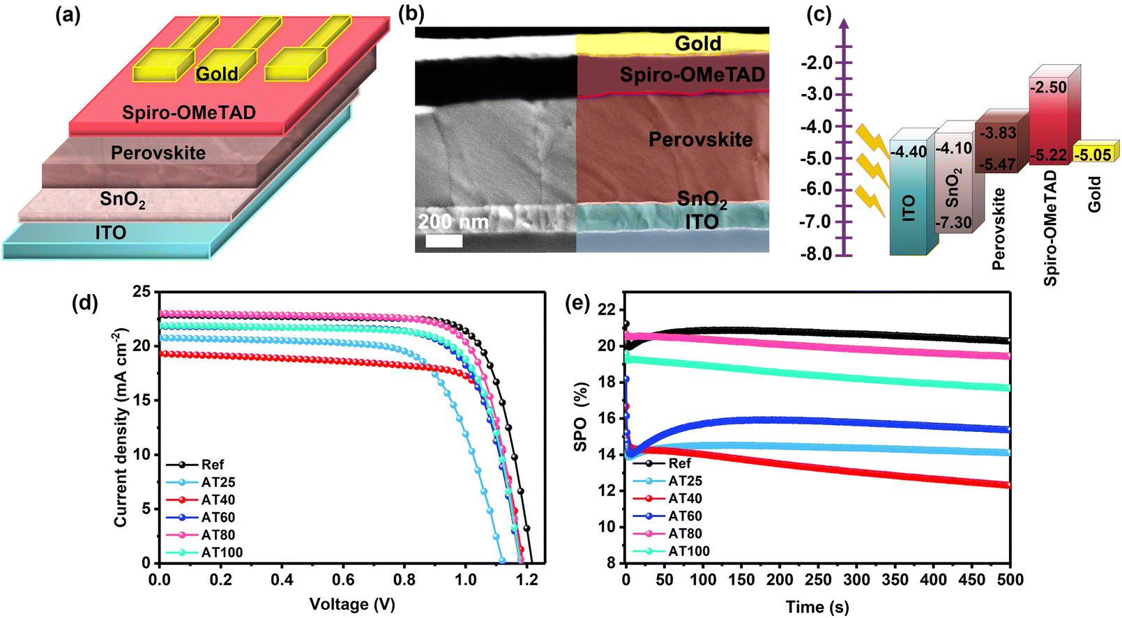 | ||
| Fig. 5 (a) Schematic of the device architecture, (b) cross-section image of PSCs fabricated by ASB annealed at 80 °C, (c) corresponding band energy diagram of fabricated PSCs, the energy level of gold is higher than the HOMO level of Spiro-OMeTAD, (d) J–V curves, and (e) SPO at 0.90, 0.78, 0.81, 0.84, 0.93, and 0.86 V for reference, AT25, AT40, AT60, AT80, and AT100 thin films of the perovskite solar devices with record performance. | ||
As shown in Fig. 5d, when the annealing temperature increased from 25 to 80 °C, an improvement in the device performance can be demonstrated from 15.9 to 20.6% and it started to decrease for a higher temperature at 100 °C (to 19.1%). With the 80 °C annealing temperature, the stabilized power output (SPO) of the champion cell reached 19.4% after 500 s comparable with the dripping antisolvent method at 20.3% (see Fig. 5e). The maximum PCE of the device based on AT80 perovskite films is achieved with an open-circuit voltage (VOC) of 1.19 V, short circuit current density (JSC) of 22.5 mA cm−2 and a fill factor (FF) of 76%. The JSC values are further verified by comparing the external quantum efficiency (EQE) spectra of the reference and AT80 devices (see Fig. S10†). The AT80 devices show a significantly higher EQE response in the visible region than the reference devices. Moreover, integrated JSC values were found to be 21.34, and 21.36 mA cm−2 for reference, and AT80 devices, respectively, which are on par with the values found from the J–V characteristics (see Table 1). For the AT100 perovskite film-based device, the PCE decreased to 19.1% because of the reduced grain sizes (304 ± 100 nm) and more randomly oriented crystals. The detailed PV parameters of each PSC obtained at different annealing temperatures are listed in Table 1. The PV performance statistics obtained from over 50 different ASB-based solar cells with different annealing temperatures are presented in Fig. S11.†
| Annealing temperature | Condition | PCE (%) | V OC (V) | J SC (mA cm−2) | FF (%) | SPO (%) |
|---|---|---|---|---|---|---|
| Ref | Record | 21.4 | 1.22 | 22.8 | 76 | 20.3 |
| Average | 20.58 ± 0.5 | 1.22 ± 0.00 | 22.2 ± 0.7 | 76 ± 1 | ||
| AT25 | Record | 15.9 | 1.12 | 20.7 | 68 | 14.1 |
| Average | 15.1 ± 0.6 | 1.17 ± 0.01 | 19.3 ± 1.3 | 66 ± 3 | ||
| AT40 | Record | 17.2 | 1.19 | 19.3 | 75 | 12.3 |
| Average | 16.7 ± 0.4 | 1.17 ± 0.01 | 20.6 ± 1.0 | 69 ± 3 | ||
| AT60 | Record | 18.8 | 1.18 | 21.8 | 73 | 15.3 |
| Average | 17.8 ± 0.3 | 1.17 ± 0.01 | 21.1 ± 0.9 | 72 ± 3 | ||
| AT80 | Record | 20.6 | 1.19 | 22.5 | 76 | 19.4 |
| Average | 19.9 ± 0.3 | 1.17 ± 0.01 | 22.5 ± 0.5 | 75 ± 2 | ||
| AT100 | Record | 19.1 | 1.18 | 21.9 | 74 | 17.7 |
| Average | 18.6 ± 0.2 | 1.17 ± 0.00 | 21.3 ± 0.6 | 73 ± 1 |
The average PCEs of the AT25, AT40, AT60, AT80, and AT100 perovskite film-based PSCs were determined to be 15.1, 16.7, 17.8, 19.9, and 18.6%, respectively. The high average PCE value for the AT80 (19.9%) perovskite film-based PSCs mainly originated from the enhanced JSC and FF from 20.6 to 22.5 mA cm−2 and from 69 to 75%, while the VOC exhibited unchanged at 1.17 V compared with that of the lower annealing temperature of 40 °C. It is worth noticing that the average FF of the AT80 perovskite film is relatively 11% higher than the AT25 PSC with the ASB method, which is consistent with the larger average grain size (444 ± 122 nm) verified by top SEM images (Fig. 4e), and lower surface roughness (29.7 nm) delivered from AFM images (Fig. S9e†), and more oriented crystals in (001) direction addressed by the XRD patterns (Fig. 3b).
Moreover, the fabricated PSCs were measured for long-term stability at AM1.5G irradiation, without encapsulation, at 40 °C and relative humidity (RH) of 35%. The normalized SPO versus irradiation time for 2000 s is shown in Fig. 6a. After exposure to these conditions, the AT25, AT40, AT60, AT80, and AT100 perovskite film-based PSCs retained over 61, 71, 83, 88, and 79% of their initial PCE after 2000 s, respectively. The stability at 80 °C annealed device retains 88% of the initial performance following the reference devices (retaining 92%), which delivers the efficacy of the ASB method in terms of scalability compared to the antisolvent approach. In addition, the long-term stability of PSCs was evaluated under dark conditions, room temperature, and 60% RH, as shown in Fig. 6b. The reference and AT80 devices showed superior stability which retained 93% and 88% of the initial PCE after 60 days, respectively. The remaining PSCs including AT25, AT40, AT60 and AT100 performed with lower stability under the same condition and retained 48, 60, 50, and 78% of the initial PCE.
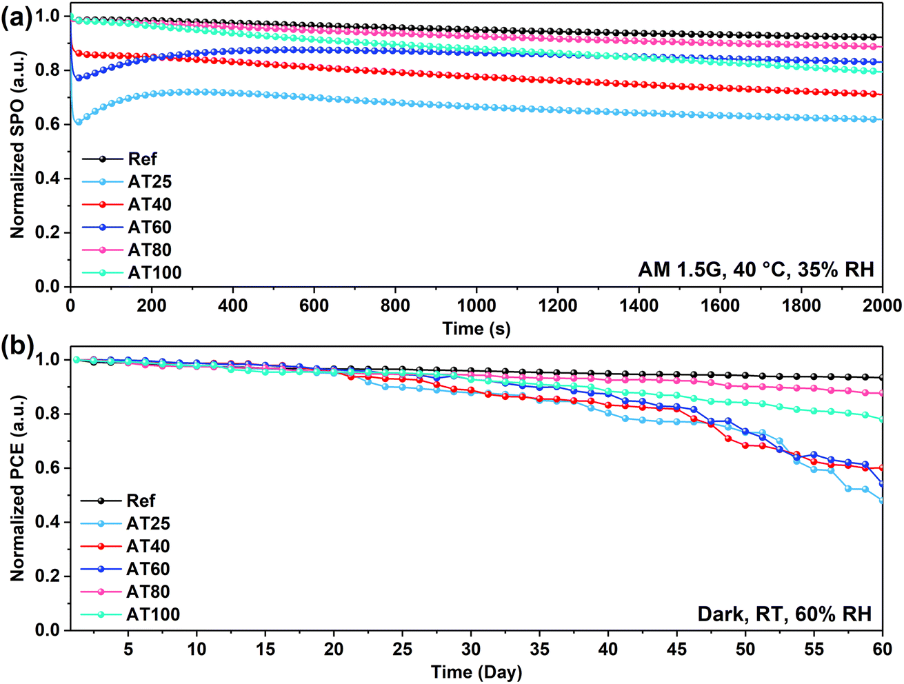 | ||
| Fig. 6 Long-term device stability (a) under AM1.5G solar irradiation, 40 °C, and 35% RH, and (b) under dark conditions, room temperature, and 60% RH, for champion PSCs based on perovskite films annealed at different temperatures in the ASB approach. | ||
2.1 Mechanism of nucleation/growth of perovskite crystals at different annealing temperatures
To further evaluate the mechanism of the DMS coordination solvent in the ASB approach and analyze the intermediate phase, Fourier-transform infrared spectroscopy (FTIR) spectra of the reference layer and perovskite films with different annealing temperatures were conducted and shown in Fig. 7a. It is worth noting that similar to the reference sample, the C–H stretching peak at 930 cm−1 is absent in the spectra of the perovskite phase with the ASB method annealed at 80 and 100 °C, which confirms the effective extraction of DMSO by DMS from the perovskite precursor solution.35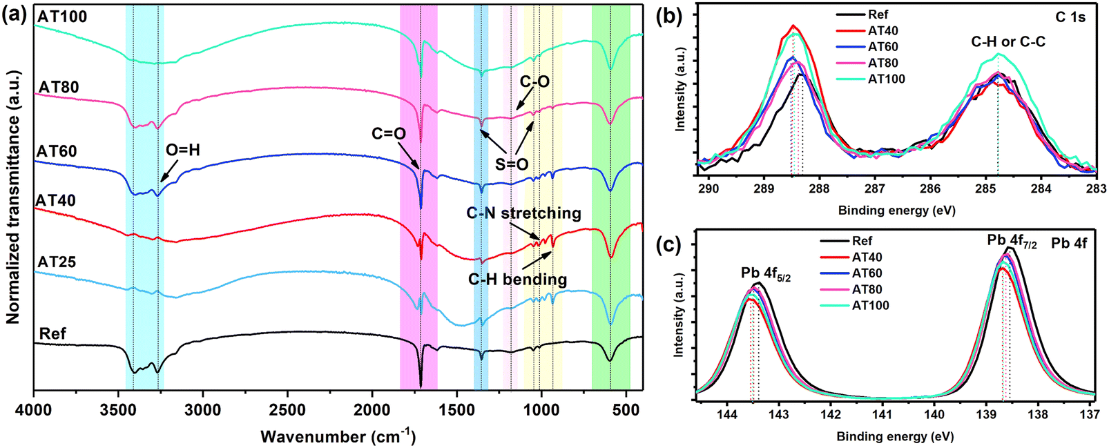 | ||
| Fig. 7 (a) FTIR spectra of reference films, and the perovskite layers with different annealing temperatures fabricated by the ASB approach, the XPS spectra of the (b) C 1s, and (c) Pb 4f regions of reference sample and perovskite layers with different annealing temperature. | ||
Moreover, X-ray photoelectron spectroscopy (XPS) was carried out to gain a deeper understanding of the electrochemical properties of perovskite material by different annealing temperatures, as shown in Fig. 7b and c. The high purity of perovskite films obtained by ASB method at AT80 is confirmed by the reduced peak at 284.7 eV of the C 1s spectrum, as it belongs to the adventitious carbon C–C or C–H bonding (Fig. 7b) which is lower, suggesting that fewer defective crystals are formed. In addition, as shown in Fig. 7c, both Pb 4f core levels shift towards higher binding energies (138.7 and 143.5 eV) for the samples obtained by the ASB approach compared to the reference films, indicating decreased electron cloud density for the Pb atom. These results demonstrate DMS could chemically interact with perovskite materials via either coordinative bonding or hydrogen bonding to passivate defects. As shown in Fig. S12,† the peak position of the core level of N 1s, and Cs 3d shifted to the higher binding energy for the AT40 films. However, after 60, 80, and 100 °C, the main peaks turned back to lower binding energy, whereas for the AT80 films, the peaks are closer to the reference one. In addition, the peak position of I 3d and Br 3d shifts to higher binding energies for different annealing temperatures, as well as compared to the reference sample, suggesting a change in the surface chemical environment. The electron diffusion length (LD), electron carrier mobility (μe), and density of defects (ntrap) were investigated by electron-only (ITO/compact-SnO2/perovskite/PC61BM/Au) devices (see the inset of Fig. 8) and space-charge-limited current (SCLC) method.
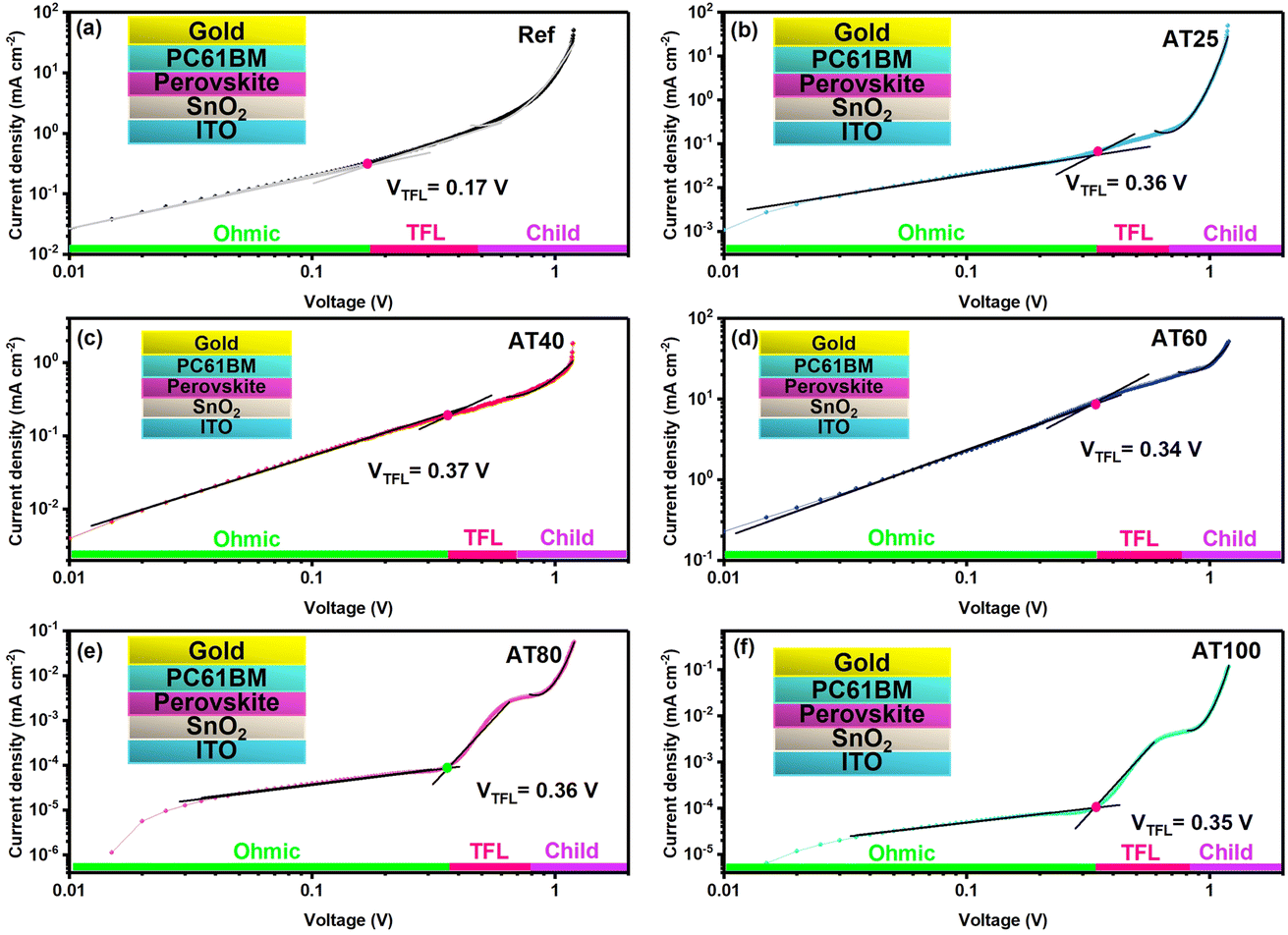 | ||
| Fig. 8 The J–V graphs of (ITO/compact-SnO2/perovskite/PC61BM/Au) devices for the (a) reference device and with different annealing temperatures of (b) 25, (c) 40, (d) 60, (e) 80, and (f) 100 °C, with the electron-only structure shown in the inset. | ||
The dark J–V curve can be separated into three different sections, including the ohmic section (J ∝ V), the trap-filling limit section (TFL section, J ∝ Vn, n > 2), and the trap-free Child section (J ∝ V2). The conductivity (σ) and the free electron carrier concentration (nc) can be extracted from the ohmic section of the J–V curve. For the ohmic section and the TFL region, the switch point between these two sections is named the trap filling limit voltage (VTFL). All traps are filled at VTFL voltage, which defines the ntrap.44 In the Child section (J ∝ V2), the μ can be calculated from the Mott–Gurney law.45 The results are shown in Table 2 (see details in ESI† for calculating LD, μe, and ntrap). Therefore, from Fig. 8, it is found that the free electron concentration (nc) is decreased for the AT80 perovskite films (8.3 × 1010 cm−3) compared to the reference device (54 × 1010 cm−3), which implies the efficient electron injection to the adjacent charge transport layers in the highly crystalline perovskite layer.
| Annealing temperature | L D (μm) | σ (Ω−1 cm−1) | n c (cm−3) | V TFL (V) | n trap (cm−3) | μ e (cm2 V−1 s−1) |
|---|---|---|---|---|---|---|
| Ref | 1.04 | 6.5 × 10⁻⁸ | 54 × 1010 | 0.17 | 0.16 × 10¹⁶ | 0.76 |
| AT25 | 1.03 | 5.7 × 10⁻⁸ | 19 × 1010 | 0.36 | 0.44 × 10¹⁶ | 1.89 |
| AT40 | 0.72 | 6.9 × 10⁻⁸ | 0.01 × 10¹⁰ | 0.37 | 0.44 × 10¹⁶ | 0.38 |
| AT60 | 1.42 | 7.4 × 10⁻⁸ | 58.7 × 10¹⁰ | 0.34 | 0.38 × 10¹⁶ | 0.79 |
| AT80 | 3.11 | 4.9 × 10⁻⁸ | 8.3 × 10¹⁰ | 0.36 | 0.37 × 10¹⁶ | 3.59 |
| AT100 | 1.80 | 4.3 × 10⁻⁸ | 6.8 × 10¹⁰ | 0.35 | 0.37 × 10¹⁶ | 3.93 |
Meanwhile, compared to the reference device, the μe of the AT80 perovskite film-based devices improved from 0.76 to 3.59 cm2 V−1 s−1. Hence, the optimized annealing at 80 °C modifies the crystalline quality and enhances the electron carrier mobility, leading to the performance improvement. It is worth mentioning that by utilizing the SCLC results, the AT80 devices delivered an LD of 3.11 μm exceeding the reference devices with an LD of 1.04 μm. Several studies have shown theoretically,46–48 and experimentally (Kelvin probe force microscopy)49 that the amorphous regions at grain boundaries of perovskite films can be beneficial for charge separation and collection,49 increasing PL intensity without degrading carrier lifetime. The long carrier LD of over 3 μm associated with the amorphous regions at the grain boundaries explains the long lifetime and record efficiency achieved in moderate grain sizes (400 nm) of 3-hal perovskite AT80 thin films. This indicates that optimized annealing leads to a trap-free pathway for more effectively transporting photogenerated charge carriers, which is consistent with an improved JSC. The FF is also enhanced, which can be ascribed to the formation of high-quality perovskite films as derived from the XRD patterns (see Fig. 3 and S3†), revealing an improvement of the charge carrier lifetime as deduced from TRPL measurements (see Fig. 2d).
3. Conclusions
Efficient and stable PSCs were developed by employing a scalable ASB approach, using the highly coordinating DMS solvent and a subsequent annealing process. Through the optimization of the annealing temperature, large grains of ∼444 ± 122 nm with a reduced photo-inactive δ-phase and PbI2 impurity were produced with a high orientation in (001) direction and uniform thin films. The efficacy of the DMS for extracting the DMSO from the perovskite precursor was demonstrated by its strong coordination of Pb 4f core level and reduced carbon impurities, which resulted in a more controllable crystallization. Due to the long charge carrier diffusion length of 3 μm and recombination lifetime of 1050 ns, as well as the morphological and crystallographic improvements in the perovskite film, the performance of the AT80 perovskite films was 20.6% comparable to the reference devices at 21.4%. This study opens the door to the scalable fabrication of highly crystalline and stable thin films for sustainable optoelectronic perovskite devices.4. Experimental section
4.1 Materials
Dimethyl sulfoxide (DMSO, anhydrous, >99.9%) and N,N-dimethylformamide (DMF, anhydrous, 99.8%), methyl acetate (MAc, anhydrous, 99.5%), dimethyl sulfide (DMS, 99%) chlorobenzene (CB, 98%), were purchased from Sigma-Aldrich. We used Mucasol alkaline cleaner solution obtained from Schülke & Mayr GmbH for substrate cleaning. The solvents including 2-propanol (IPA), ethanol, and acetone were obtained from VWR International Ltd. The perovskite cation precursors including formamidinium iodide (FAI, 99.99%, trace elements basis) and formamidinium chloride (FACl, 99.98%, trace elements basis) were purchased from Greatcellsolar, lead(II) iodide (PbI2, 99.99%, trace metals basis), lead(II) bromide (PbBr2), and lead(II) chloride (PbCl2) were purchased from TCI. The cesium iodide (CsI, 99.999%, metal basis) was provided by abcr GmbH. The HTM 2,2′,7,7′-tetrakis-(N,N-di-4-methoxyphenylamino)-9′-spirobifluorene (Spiro-OMeTAD) and phenyl-C61-butyric acid methyl ester (PC61BM, >99.5%) was obtained from Lumtec. The additives for Spiro-OMeTAD such as lithium bis(trifluoromethanesulfonyl)imide (Li-TFSI), 4-tertbutylpyridine (TBP), and tris(2-(1H-pyrazol-1-yl)-4-tert-butylpyridine)-cobalt(III)tris(bis(trifluoromethylsulfonyl)imide)) (FK209) were purchased from Sigma Aldrich. For the metallization process, gold nuggets were used.4.2 Device fabrication
4.2.3.1 FAPbI3. The FAPbI3 stock solution was prepared by dissolving FAI powder with a PbI2 stock solution (2 M, 10% excess of Pb) in anhydrous DMF
![[thin space (1/6-em)]](https://www.rsc.org/images/entities/char_2009.gif) :DMSO 4:1 (v/v) and diluting to 1.6 M.
:DMSO 4:1 (v/v) and diluting to 1.6 M.
4.2.3.2 CsI. A CsI stock solution (2 M) was prepared by dissolving CsI powder in anhydrous DMSO at 150 °C for 10 min.
4.2.3.3 PbBr2. PbBr2 solution (2 M), prepared in anhydrous DMF
:DMSO 4:1 (v/v) at 150 °C for 10 min.
4.2.3.4 FAPbCl3. FAPbCl3 solution (1.28 M) was prepared by dissolving FACl powder with a PbCl2 stock solution (1.5 M) in anhydrous DMSO.
The mixed-halide perovskite (3-hal) solution was prepared by mixing the corresponding volumes of the above FAPbI3, CsI, PbBr2, and FAPbCl3 solutions.
4.3 Characterization
Data availability
The data supporting the article have been included as part of the ESI.†Author contributions
M. S. directed and supervised the research. S. G., M. M. B., and M. S. did the conceptualization and provided the expertise and design of the method. J. J. J.-R. wrote the first draft of the manuscript under the guidance of M. M. B. and M. S., designed the experiments, and was responsible for device fabrication and data interpretation. S. G. helped with the schematics, figures, and tables. S. S. assisted with the PL and TRPL measurements. R. R. helped with the FTIR measurements. S. B. and S. T. measured SEM and EDX analysis. W. Z., M. Z., and M. A. helped with the reviewing and editing. M. K. measured XRD. A. Z. and A. G. R. did AFM and XPS measurements. S.-H. T.-C., P. S., M. S. guided the project discussions, reviewing, and editing. All co-authors participated in the discussion and reviewed the manuscript.Conflicts of interest
There are no conflicts to declare.Acknowledgements
S.-H. T.-C. gratefully acknowledges funding from the Ministry of Science and Innovation of Spain under Ayudas Ramón y Cajal (RYC2022-035578-I) and the POLONEZ Bis project No. 2021/43/P/ST5/01780 co-funded by the National Science Centre and the European Union's Horizon 2020 research and innovation program under the Marie Skłodowska-Curie grant agreement no. 945339 for the financial support during this work. A. G. R. and P. S. acknowledge Agence Nationale de la Recherche through the Interdisciplinary Thematic Institute SysChem via the IdEx Unistra (ANR-10-IDEX-0002) within the program Investissement d’Avenir, the Foundation Jean-Marie Lehn and the Institut Universitaire de France (IUF). M. S. thanks the German Research Foundation (DFG) for funding (SPP2196, 431314977/GRK 2642). M. S., and M. M. B. thank Helmholtz Young Investigator Group FRONTRUNNER. M. S. acknowledges funding from the European Research Council under the Horizon Europe programme (LOCAL-HEAT, grant agreement no. 101041809). The views and opinions expressed are solely those of the authors and do not necessarily reflect those of the European Union or the European Research Council. Neither the European Union nor the granting authority can be held responsible for them. M. S. acknowledges funding from the German Bundesministerium für Bildung and Forschung (BMBF), project “NETPEC” (01LS2103E).References
- B. Xia, M. Tu, B. Pradhan, F. Ceyssens, M. L. Tietze, V. Rubio-Giménez, N. Wauteraerts, Y. Gao, M. Kraft, J. A. Steele, E. Debroye, J. Hofkens and R. Ameloot, Adv. Eng. Mater., 2022, 24, 2100930 CrossRef.
- V. Sharma and P. K. Jha, Sol. Energy Mater. Sol. Cells, 2019, 200, 109908 CrossRef.
- M. Nadafan, Z. Dehghani, Z. Shadrokh and Y. Abdi, Opt Laser. Technol., 2023, 160, 109055 CrossRef.
- X. Liu, Y. Wang, Y. Wang, Y. Zhao, J. Yu, X. Shan, Y. Tong, X. Lian, X. Wan, L. Wang, P. Tian and H.-C. Kuo, Nanotechnol. Rev., 2022, 11, 3063–3094 CrossRef.
- B. Liu, Y. Wang, Y. Wu, B. Dong and H. Song, J. Mater. Sci. Technol., 2023, 140, 33–57 CrossRef.
- S. Shrestha, X. Li, H. Tsai, C.-H. Hou, H.-H. Huang, D. Ghosh, J.-J. Shyue, L. Wang, S. Tretiak, X. Ma and W. Nie, Chem, 2022, 8, 1107–1120 Search PubMed.
- J. Lim, M. Kober-Czerny, Y.-H. Lin, J. M. Ball, N. Sakai, E. A. Duijnstee, M. J. Hong, J. G. Labram, B. Wenger and H. J. Snaith, Nat. Commun., 2022, 13, 4201 Search PubMed.
- K. R. Hansen, C. E. McClure, D. Powell, H.-C. Hsieh, L. Flannery, K. Garden, E. J. Miller, D. J. King, S. Sainio, D. Nordlund, J. S. Colton and L. Whittaker-Brooks, Adv. Opt. Mater., 2022, 10, 2102698 CrossRef.
- Z. Saki, M. M. Byranvand, N. Taghavinia, M. Kedia and M. Saliba, Energy Environ. Sci., 2021, 14, 5690–5722 RSC.
- J. J. Jeronimo-Rendon, S.-H. Turren-Cruz, J. Pascual, D. D. Girolamo, M. A. Flatken, H. Köbler, W. Hempel, M. Li, A. D. Carlo, P. P. Boix, I. Mora-Seró, A. Abate and M. Saliba, Adv. Funct. Mater., 2024, 34, 2313928 CrossRef.
- M. M. Elshanawany, A. G. Ricciardulli, J. J. Jeronimo-Rendon, M. Saliba, J. Wachtveitl and M. Braun, J. Phys. Chem. C, 2022, 126, 8787–8793 CrossRef.
- Y. Chen, S. G. Motti, R. D. J. Oliver, A. D. Wright, H. J. Snaith, M. B. Johnston, L. M. Herz and M. R. Filip, J. Phys. Chem. Lett., 2022, 13, 4184–4192 CrossRef PubMed.
- Z. Wang, C. Shan, C. Liu, X. Tang, D. Luo, H. Tang, Z. Song, J. Wang, Z. Ren, J. Ma, H. Wang, J. Sun, N. Zhang, W. C. H. Choy, Y. Liu, A. K. K. Kyaw, X. W. Sun, D. Wu and K. Wang, Cell Rep. Phys. Sci., 2023, 4, 101363 CrossRef.
- Y. Kumar, E. Regalado-Perez, J. J. Jerónimo-Rendón and X. Mathew, Sol. Energy Mater. Sol. Cells, 2022, 236, 111512 CrossRef CAS.
- X. Zhang, M. E. Turiansky, J.-X. Shen and C. G. Van de Walle, J. Appl. Phys., 2022, 131, 090901 CrossRef CAS.
- I. du Fossé, J. T. Mulder, G. Almeida, A. G. M. Spruit, I. Infante, F. C. Grozema and A. J. Houtepen, J. Am. Chem. Soc., 2022, 144, 11059–11063 CrossRef PubMed.
- S. Liu, J. Li, W. Xiao, R. Chen, Z. Sun, Y. Zhang, X. Lei, S. Hu, M. Kober-Czerny, J. Wang, F. Ren, Q. Zhou, H. Raza, Y. Gao, Y. Ji, S. Li, H. Li, L. Qiu, W. Huang, Y. Zhao, B. Xu, Z. Liu, H. J. Snaith, N.-G. Park and W. Chen, Nature, 2024, 1–3 Search PubMed.
- Best Research-Cell Efficiency Chart | Photovoltaic Research, NREL, Golden, CO, USA, 2024 Search PubMed.
- G. Burwell, S. Zeiske, P. Caprioglio, O. J. Sandberg, A. M. Kay, M. D. Farrar, Y. R. Kim, H. J. Snaith, P. Meredith and A. Armin, Sol. RRL, 2024, 2400180 CrossRef CAS.
- H. Sun, S. Liu, X. Liu, Y. Gao, J. Wang, C. Shi, H. Raza, Z. Sun, Y. Pan, Y. Cai, S. Zhang, D. Sun, W. Chen and Z. Liu, Small Methods, 2024, 8, 2400067 CrossRef CAS.
- L. Yang, Z. Fang, Y. Jin, H. Feng, B. Deng, L. Zheng, P. Xu, J. Chen, X. Chen, Y. Zhou, C. Shi, W. Gao, J. Yang, X. Xu, C. Tian, L. Xie and Z. Wei, Adv. Mater., 2024, 36, 2311923 CrossRef CAS.
- J. Xu, C. C. Boyd, Z. J. Yu, A. F. Palmstrom, D. J. Witter, B. W. Larson, R. M. France, J. Werner, S. P. Harvey, E. J. Wolf, W. Weigand, S. Manzoor, M. F. A. M. van Hest, J. J. Berry, J. M. Luther, Z. C. Holman and M. D. McGehee, Science, 2020, 367, 1097–1104 CrossRef CAS PubMed.
- T. Nie, Z. Fang, X. Ren, Y. Duan and S. F. Liu, Nano-Micro Lett., 2023, 15, 70 CrossRef CAS.
- R. Rahighi, S. Gholipour, M. A. Amin and M. Z. Ansari, Nanomaterials, 2023, 13, 1417 Search PubMed.
- G. Li, Z. Su, L. Canil, D. Hughes, M. H. Aldamasy, J. Dagar, S. Trofimov, L. Wang, W. Zuo, J. J. Jerónimo-Rendon, M. M. Byranvand, C. Wang, R. Zhu, Z. Zhang, F. Yang, G. Nasti, B. Naydenov, W. C. Tsoi, Z. Li, X. Gao, Z. Wang, Y. Jia, E. Unger, M. Saliba, M. Li and A. Abate, Science, 2023, 379, 399–403 CrossRef PubMed.
- M. Hatamvand, S. Gholipour, M. Chen, Y. Zhou, T. Jiang, Z. Hu, Y. Chen and W. Huang, Chem. Eng. J., 2023, 141788 CrossRef.
- A. D. Taylor, Q. Sun, K. P. Goetz, Q. An, T. Schramm, Y. Hofstetter, M. Litterst, F. Paulus and Y. Vaynzof, Nat. Commun., 2021, 12, 1878 CrossRef PubMed.
- Y. Y. Kim, T.-Y. Yang, R. Suhonen, A. Kemppainen, K. Hwang, N. J. Jeon and J. Seo, Nat. Commun., 2020, 11, 5146 CrossRef PubMed.
- Y. Zhou, M. Yang, W. Wu, A. L. Vasiliev, K. Zhu and N. P. Padture, J. Mater. Chem. A, 2015, 3, 8178–8184 RSC.
- G. R. Adams, V. O. Eze, L. B. Carani, A. Pino, C. Jolowsky and O. I. Okoli, RSC Adv., 2020, 10, 18139–18146 RSC.
- G. Jang, S. Ma, H.-C. Kwon, S. Goh, H. Ban, J. Lee, C. Uk Lee and J. Moon, Chem. Eng. J., 2021, 423, 130078 CrossRef.
- G. Jang, H.-C. Kwon, S. Ma, S.-C. Yun, H. Yang and J. Moon, Adv. Energy Mater., 2019, 9, 1901719 CrossRef.
- W. Zuo, W. Fu, K. Wang, C. Das, M. Malekshahi Byranvand, K.-L. Wang, A. Chaudhary, J. Lim, M. Li and M. Saliba, Energy Environ. Sci., 2024, 17, 1407–1415 RSC.
- B. Li, D. Gao, S. A. Sheppard, W. D. J. Tremlett, Q. Liu, Z. Li, A. J. P. White, R. K. Brown, X. Sun, J. Gong, S. Li, S. Zhang, X. Wu, D. Zhao, C. Zhang, Y. Wang, X. C. Zeng, Z. Zhu and N. J. Long, J. Am. Chem. Soc., 2024, 146, 13391–13398 CrossRef PubMed.
- W. Zuo, M. M. Byranvand, T. Kodalle, M. Zohdi, J. Lim, B. Carlsen, T. Magorian Friedlmeier, M. Kot, C. Das, J. I. Flege, W. Zong, A. Abate, C. M. Sutter-Fella, M. Li and M. Saliba, Adv. Mater., 2023, 35, 2302889 CrossRef PubMed.
- B. J. Foley, S. Cuthriell, S. Yazdi, A. Z. Chen, S. M. Guthrie, X. Deng, G. Giri, S.-H. Lee, K. Xiao, B. Doughty, Y.-Z. Ma and J. J. Choi, Nano Lett., 2018, 18, 6271–6278 CrossRef PubMed.
- A. de Peyster, in Encyclopedia of Toxicology, ed. P. Wexler, Academic Press, Oxford, 3rd edn, 2014, pp. 281–284 Search PubMed.
- S. Dutt, A. Trivedi, O. V. Rambadey, P. R. Sagdeo and A. Sagdeo, J. Mater. Sci., 2024, 59, 15449–15468 CrossRef.
- R. Prasanna, A. Gold-Parker, T. Leijtens, B. Conings, A. Babayigit, H.-G. Boyen, M. F. Toney and M. D. McGehee, J. Am. Chem. Soc., 2017, 139, 11117–11124 CrossRef PubMed.
- E. Mosconi, P. Umari and F. D. Angelis, Phys. Chem. Chem. Phys., 2016, 18, 27158–27164 RSC.
- J. Ye, Z. Li, D. J. Kubicki, Y. Zhang, L. Dai, C. Otero-Martínez, M. A. Reus, R. Arul, K. R. Dudipala, Z. Andaji-Garmaroudi, Y.-T. Huang, Z. Li, Z. Chen, P. Müller-Buschbaum, H.-L. Yip, S. D. Stranks, C. P. Grey, J. J. Baumberg, N. C. Greenham, L. Polavarapu, A. Rao and R. L. Z. Hoye, J. Am. Chem. Soc., 2022, 144, 12102–12115 CrossRef PubMed.
- B. Roose, K. Dey, Y.-H. Chiang, R. H. Friend and S. D. Stranks, J. Phys. Chem. Lett., 2020, 11, 6505–6512 CrossRef PubMed.
- A. G. Ricciardulli, S. Yang, N. B. Kotadiya, G.-J. A. H. Wetzelaer, X. Feng and P. W. M. Blom, Adv. Electron. Mater., 2019, 5, 1800687 CrossRef.
- R. H. Bube, J. Appl. Phys., 1962, 33, 1733–1737 CrossRef.
- O. Almora, D. Miravet, M. García-Batlle and G. Garcia-Belmonte, Appl. Phys. Lett., 2021, 119, 242107 CrossRef.
- J. Haruyama, K. Sodeyama, L. Han and Y. Tateyama, J. Phys. Chem. Lett., 2014, 5, 2903–2909 CrossRef PubMed.
- T. J. Jacobsson, J.-P. Correa-Baena, E. Halvani Anaraki, B. Philippe, S. D. Stranks, M. E. F. Bouduban, W. Tress, K. Schenk, J. Teuscher, J.-E. Moser, H. Rensmo and A. Hagfeldt, J. Am. Chem. Soc., 2016, 138, 10331–10343 CrossRef PubMed.
- Q. Chen, H. Zhou, T.-B. Song, S. Luo, Z. Hong, H.-S. Duan, L. Dou, Y. Liu and Y. Yang, Nano Lett., 2014, 14, 4158–4163 CrossRef PubMed.
- J. S. Yun, A. Ho-Baillie, S. Huang, S. H. Woo, Y. Heo, J. Seidel, F. Huang, Y.-B. Cheng and M. A. Green, J. Phys. Chem. Lett., 2015, 6, 875–880 CrossRef PubMed.
Footnote |
| † Electronic supplementary information (ESI) available. See DOI: https://doi.org/10.1039/d4el00018h |
| This journal is © The Royal Society of Chemistry 2025 |