
 Open Access Article
 This Open Access Article is licensed under a
 Creative Commons Attribution 3.0 Unported Licence
Micro- and milli-fluidic sample environments for in situ X-ray analysis in the chemical and materials sciences
Mark A.
Levenstein
 *,
Corinne
Chevallard
,
Florent
Malloggi
,
Fabienne
Testard
and
Olivier
Taché
*,
Corinne
Chevallard
,
Florent
Malloggi
,
Fabienne
Testard
and
Olivier
Taché
Université Paris-Saclay, CEA, CNRS, NIMBE, LIONS, 91191, Gif-sur-Yvette, France. E-mail: mark.levenstein@cea.fr
First published on 8th January 2025
Abstract
X-ray-based methods are powerful tools for structural and chemical studies of materials and processes, particularly for performing time-resolved measurements. In this critical review, we highlight progress in the development of X-ray compatible microfluidic and millifluidic platforms that enable high temporal and spatial resolution X-ray analysis across the chemical and materials sciences. With a focus on liquid samples and suspensions, we first present the origins of microfluidic sample environments for X-ray analysis by discussing some alternative liquid sample holder and manipulator technologies. The bulk of the review is then dedicated to micro- and milli-fluidic devices designed for use in the three main areas of X-ray analysis: (1) scattering/diffraction, (2) spectroscopy, and (3) imaging. While most research to date has been performed at synchrotron radiation facilities, the recent progress made using commercial and laboratory-based X-ray instruments is then reviewed here for the first time. This final section presents the exciting possibility of performing in situ and operando X-ray analysis in the ‘home’ laboratory and transforming microfluidic and millifluidic X-ray analysis into a routine method in physical chemistry and materials research.
 Mark A. Levenstein | Mark A. Levenstein is a research scientist at the French Alternative and Atomic Energy Commission (CEA). He completed his PhD at the University of Leeds (UK) on the development of micro- and milli-fluidic devices for synchrotron and laboratory-based X-ray analysis of crystallization processes. After a postdoctoral position at the University of Illinois Urbana-Champaign (USA) on the design of cementitious materials for ecosystem restoration, Mark joined the Interdisciplinary Laboratory on Supramolecular and Nanometric Organization (LIONS). His current research is focused on developing automated synthesis and characterization platforms for the discovery of sustainable materials with applications in energy, electronics, and construction. |
 Corinne Chevallard | Corinne Chevallard is a research director at CEA (France). She holds a PhD in physics from the University of Nice-Sophia-Antipolis (France). Her early research focused on instabilities in complex systems, whether liquid crystals (PhD) or polymers (postdoc at the Weizmann Institute of Science, Israel). Since joining the CEA, her research has focused on inorganic crystallization, particularly in relation to biomineralization. In order to characterize the transient structures formed prior to crystallization, she is developing microfluidic devices specifically designed for synchrotron-based techniques, which enable in situ structural and chemical characterization in liquid media at the nanoscale. |
 Florent Malloggi | Dr. Florent Malloggi received his PhD from Paris Cité University (formerly Paris VII) in 2006, specializing in the physics of liquids. He now serves as a research director in the Nanoscience and Innovation for Materials, Biomedicine and Energy (NIMBE) department of CEA within Paris-Saclay University. His research interests are focused on instrumental microfluidic development for applications in energy, chemistry and biology. |
 Fabienne Testard | Dr. Fabienne Testard is a research director at CEA, working in the LIONS Laboratory of NIMBE. She has expertise in soft-matter, self-assembling systems and nanomaterials with a strong background in synthesis, characterization and the study of the formation mechanisms of nanomaterials (mainly gold and organic self-assembled particles). She is particularly interested by the behavior of nanomaterials in complex systems and in situ SAXS and SANS approaches (with extensive experience at synchrotrons and neutron sources). |
 Olivier Taché | Olivier Taché is a researcher at CEA/NIMBE/LIONS and an expert on the characterization and metrology of nanomaterials. His work includes the development of advanced SAXS methodologies and software to enhance the precision and reliability of nanoparticle size and concentration measurements. He is actively involved in various collaborative projects aimed at enhancing nanosafety and the traceability of nanomaterial measurements. |
1 Introduction
There remain many fundamental questions in the chemical and materials sciences relating to natural phenomena and industrial processes including the nucleation and growth pathways of materials,1,2 the function and deactivation of catalysts,3,4 and the operation and failure modes of batteries.5–7 X-rays seem ideally suited to provide insight into these areas since they facilitate a suite of structural, chemical, and imaging techniques, offer high spatial and temporal resolution, and have the penetrating ability required to make in situ or operando observations within thick three-dimensional (3D) samples. These strengths have only increased in recent years due to the widespread availability of third generation synchrotron light sources,8 the arrival of X-ray free electron lasers (XFELs) and fourth generation synchrotrons,9,10 and large improvements in commercial X-ray instruments.11 However, for many types of samples, one bottleneck is introducing the analyte into the X-ray beam in a way that fully exploits these attributes: for example, rapidly and uniformly mixing liquid reagents to initiate a reaction within the short timescales required to make a single measurement.Microfluidic devices have been proposed as one solution to this sample preparation and manipulation problem. In an excellent earlier review in this journal, Ghazal et al. covered the benefit of microfluidics for X-ray analysis in the life sciences and soft matter research.12 Their review was primarily focused on the ways microfluidic devices could be used to produce and manipulate large numbers of samples and make better use of experimental time at synchrotron facilities. They also highlighted the ways that microfluidic devices could be utilized to perform time-resolved measurements of processes not accessible by conventional macroscale methods. Here, we seek to build upon their work by covering applications in physical chemistry and materials science and focusing primarily on the role of microfluidic devices as “sample environments”. We define these as specialized devices and reactors that enable in situ or operando measurements of samples and processes in their native states or under non-equilibrium conditions. For the purposes of this review, in situ means that a measurement is performed where the reaction or process takes place without moving the sample into a second holder or vessel, and operando means that a measurement is performed both in situ and while the reaction or process is occurring. By this definition, all operando measurements are in situ, but not all in situ measurements are operando. This is not necessarily the same definition as used in catalysis literature.13 The opposite would then be ex situ or post-mortem analysis, where a sample must be moved out of its native environment and prepared for measurement, often requiring quenching, washing, and drying steps, among others.14
A growing interest across the chemical, physical, and natural sciences is the study of processes in real-time. For processes that are difficult to observe in nature (e.g., high-pressure phenomena in the Earth's interior) or in industrial environments (e.g., within large chemical reactors), these conditions need to be re-created in the laboratory. Microfluidic and other miniaturized devices present a promising way to achieve these goals owing to their ability to control heat and mass transport phenomena quickly and precisely and due to their increased safety over macroscale methods when working under extreme temperatures, pressures, and chemical conditions. Here, our analysis is not restricted to microfluidic devices with channel dimensions ≪1 mm, because as many have correctly highlighted,12,15 a longer X-ray beam pathlength through samples results in an optimized signal-to-noise ratio (≈1 mm with aqueous solutions and Cu Kα radiation). Therefore, for some applications, millifluidic sample environments may even be preferred over their microfluidic counterparts.
Despite a handful of earlier papers, such as on the microfluidic preparation of crystals for subsequent off-chip X-ray diffraction,16,17 it may have been Greaves and Manz (2005) who first recognized the potential of microfluidic devices for on-chip chemical X-ray analysis.18 They highlighted, in particular, the power of X-ray fluorescence and X-ray diffraction for elemental analysis and particle identification in flow, respectively, and anticipated that performing real-time measurements on-chip could reduce the time required to optimize crystallization and synthesis conditions. While they did investigate on-chip X-ray generation to make a true “lab-on-a-chip”, they also realized that microfluidic devices could serve as powerful complements to full-scale laboratory equipment, and this is precisely the direction in which the field of microfluidic X-ray analysis has gone over the past 20 years. In fact, in this context, microfluidic devices have been coupled to some of the largest scientific instruments in existence: synchrotron particle accelerators and free-electron lasers. This striking combination of the very big and the very small, already inherent in such facilities, offers the possibility of combining the precise manipulation of subatomic particles with that of molecules and nano- and micro-objects in flow. In addition to this, the control of flow can also solve practical problems like mitigating radiation-induced sample damage and heating, which is becoming more and more important as X-ray sources grow stronger.19
Our goal with this review is to provide as comprehensive of an account as possible into the use of micro- and milli-fluidic sample environments for in situ X-ray analysis in the physical and chemical sciences. Therefore, we will cover applications across the three main types of X-ray techniques: scattering/diffraction (section 3), spectroscopy (section 4), and imaging/tomography (section 5). There are many commonalities in the design considerations and technical challenges of sample environments for these different techniques, and we believe that the communities around each technique could benefit from the sharing of knowledge. Preceding this central part of the review, we will also provide some background on predecessor and alternative sample environments for in situ X-ray studies in liquids and a brief discussion of some important parameters to consider in relation to microfluidic sample environments (section 2).
As already mentioned, due to the need for fast measurements of dynamic and often dilute samples, microfluidic X-ray experiments are typically performed at synchrotron light sources and sometimes XFELs. These facilities are operated on a competitive, proposal-based, user access model where individual beamlines or end-stations dedicated to scattering, spectroscopy, imaging, or a combination of techniques must be solicited for experimental time. Further, these facilities are seldom located near a researcher's home institution. Therefore, experimental “beamtime” is not guaranteed, not limitless, and often not easy in terms of the transport and set-up of complex equipment. Near the end of the review, we will thus cover progress in utilizing micro- and milli-fluidic sample environments with laboratory X-ray instruments (section 6), where techniques such as X-ray diffraction (XRD), X-ray fluorescence (XRF), and micro-computed tomography (μCT) are already readily available at most universities and research institutes. The increasing feasibility of laboratory-based analysis should facilitate much easier and more practical in situ X-ray experiments. It should also allow many more researchers to benefit from fluidic X-ray sample environments in their own research, when the high brilliance or coherence provided by large-scale X-ray facilities is not strictly required. Finally, we will present our perspective on the current state of the field and some practical tips regarding device fabrication and best practices (section 7). This will conclude with a look towards the future focused on promising trends and developments that we think will guide the field over the coming years.
This review will be limited to micro- and milli-fluidic X-ray sample environments where measurements are performed in situ, on-chip, and on inorganic and/or hard condensed matter samples. Articles pertaining to only biological or soft condensed matter samples, such as those already reviewed by Ghazal et al.,12 will be referenced only where they have made an important technical contribution later implemented for physical chemistry or materials research. An exception will be made in section 6 on laboratory-based analysis, where studies of all sample types will be covered, since these have not been reviewed previously. Similarly, articles where analysis is performed on a droplet, jet, or spray exiting a microfluidic device will also be excluded, although some will be introduced briefly in the background section. Such jet-based devices have been covered previously in the context of serial crystallography, and the reader is directed to these reviews for further information.20–22 To the best of our ability, this review is comprehensive up through the year 2023 unless otherwise noted.
2 Background
This background section is not intended to be exhaustive, rather its goal is to provide some general context for the review. It will focus on two important pre-microfluidic technologies and two important microfluidics-parallel technologies, all of which remain in use today and have weaknesses—and also some strengths—compared to microfluidics. This will provide the reader with the setting in which micro- and milli-fluidic sample environments operate and a general knowledge of the types of liquid sample manipulation tools currently available at large-scale X-ray facilities. We will finally present some design considerations and definitions for describing micro- and milli-fluidic flow reactors and their utility for in situ X-ray analysis, which will aid in evaluating and comparing the devices presented in the following review.2.1 Precursors to microfluidic devices
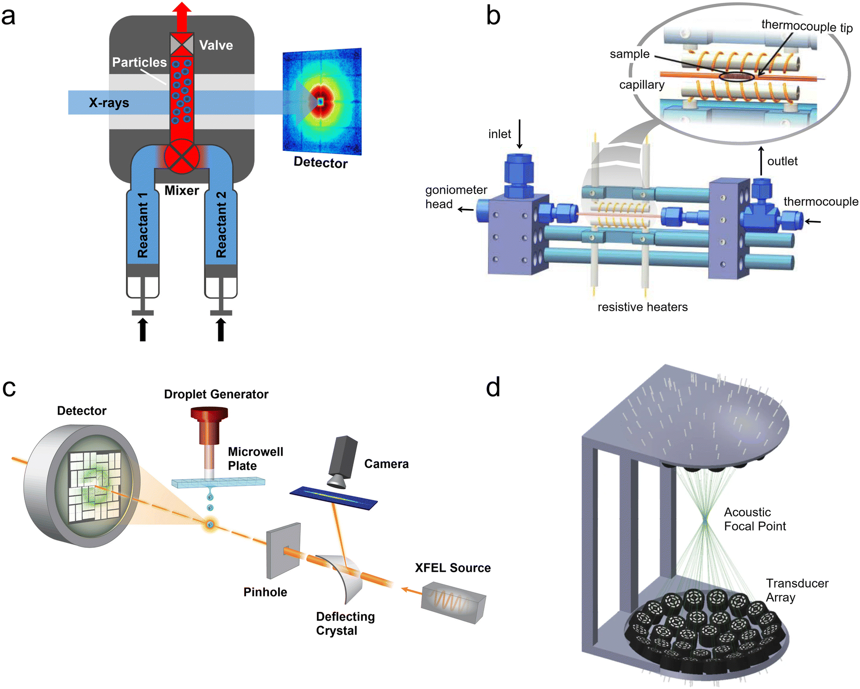 | ||
| Fig. 1 Predecessors and alternatives to micro- and milli-fluidic devices for X-ray analysis. (a) Illustration of a stopped-flow device mounted at an X-ray scattering facility. Two reactants are injected through a mixing element into a capillary where the flow is stopped by a fast valve (adapted with permission from Virtanen et al., 2019; Copyright 2019 American Chemical Society).26 (b) Design of a capillary gas cell with flow and heating capabilities. The inset shows a detailed view of the capillary where the powder sample is placed (adapted with permission from Chupas et al., 2008; International Union of Crystallography).37 (c) A droplet injector for use with XFELs. Each droplet is hit by a single femtosecond X-ray laser pulse (adapted from Roessler et al., 2016; with permission from Elsevier).38 (d) Design of a droplet levitator comprising acoustic transducer arrays to position a liquid sample at a focal point within an X-ray beam (adapted with permission from Morris et al., 2019; CC BY).39 | ||
The popularity and longevity of the stopped-flow method likely stem from its accessible operation yet powerful performance. Originally developed in the 1940s, stopped-flow devices required a much smaller volume of solution than their large continuous flow predecessors.25,40 Utilizing passive turbulent mixers, such as the Ball-Berger design,41 stopped-flow devices can also achieve mixing times in the 1 ms to 0.01 ms range (with dead times before observation from ∼10 ms down to 0.1 ms).42 From a practical standpoint, many off-the-shelf commercial devices exist, which are often available at synchrotron beamlines and already integrated with beamline hardware and acquisition software. While they are not always simple to use, they may be easier to work with than many home-made devices.
Despite these numerous strengths, stopped-flow devices have some weaknesses that are especially pronounced in the case of X-ray analysis. One is that the time-resolution of the measurements is limited by the duration of X-ray exposure required to achieve a good signal-to-noise ratio. Taking X-ray scattering as an example, the small number of photons elastically scattered compared to the number of photons in the incident beam often requires the use of high-brilliance synchrotron radiation. However, even at many current beamlines, it is difficult to obtain a good quality small angle X-ray scattering (SAXS) pattern from exposures much shorter than 0.02–1 s (i.e., frame rates of 1–50 Hz) depending on the sample contrast. This is especially true at early reaction times of less than a few seconds, when weakly scattering and/or dilute reaction intermediates—requiring even longer exposures to be detected—are present. Moreover, longer exposure times are also required for performing wide-angle X-ray scattering (WAXS).
One solution to this first weakness of stopped-flow devices is to average the results of several experiments. However, combining individual time-resolved frames from different experiments requires very high reproducibility in the mixing conditions, the cleaning procedure, and the timing between the data acquisition workflow and the operation of the device. This is not always the case due to, for example, the formation of bubbles during mixing and inconsistencies in the mixing ratio.43 Another solution, such as increasing the photon flux, only highlights another weakness of stopped-flow devices. This is that the sample is retained in the capillary and continually exposed to high energy ionizing radiation. Depending on the sensitivity of the sample, it is possible that radiation-induced heating or beam damage could alter the process under study and introduce significant uncertainty into data interpretation. Indeed, this problem can even affect inorganic materials,44,45 and it has only increased at fourth generation synchrotrons.19
Capillary gas cells are powerful sample environments that enable a range of in situ and operando studies under extreme conditions. These include investigations of hydrothermal synthesis,49,50 catalysis,48,51 gas capture and storage,52 solid phase transformations,53 and other gas–solid interactions.54 As already stated, their simplicity, ubiquity, and utilization of commercial components make them attractive to many researchers, however, they do have some weaknesses. They are primarily designed to interact with a pre-loaded powder, slurry, or sample bed that is fixed in place. Outside of a few exceptions, in situ generation of the sample (e.g., synthesis from solution) or subsequent manipulation or interaction (e.g., fluid injection) with the sample is not supported. There are versions of the capillary cell that enable high pressure liquid flows, but these are essentially large millifluidic systems55,56—although they will not be treated further here. Even considering these exceptions, reaction products are still not recycled under the beam, presenting the same potential for radiation damage as stopped-flow devices. Additionally, the high temperature and pressure of the gas cells and the fragility of the glass capillaries present a safety risk that must be considered during the experiment.52,55
2.2 Parallel technologies
Injector-based serial femtosecond crystallography (SFX) was first demonstrated by Chapman et al.57 using a gas dynamic virtual nozzle (GDVN),58 which can be tuned to produce jets or monodisperse droplets with the use of a piezoelectric actuator. A very fast (∼10–100 m s−1) and thin (∼1–25 μm diameter) fluid jet is created by a high flow rate of sample (typically protein crystals in their mother liquor) surrounded by a sheath flow of a low density gas (e.g., He) in order to rapidly replenish the sample stream after each X-ray pulse (up to MHz frequency).59 However, for rare or expensive samples the amount of liquid consumed to maintain this jet is too high, and utilizing crystals grown and injected in viscous lipidic cubic phases (LCPs) was later shown to enable jet formation at lower flow rates, reducing sample consumption by a factor of 20.60 Other groups have developed drop-on-demand systems, such as acoustic injectors that can dose nanoliter to picoliter droplets directly from a microwell plate (Fig. 1c).38 While many of the uses of these XFEL injector systems have focused on structural biology, they have also facilitated fundamental physics and chemistry experiments including investigating the ionization61 and supercooling of water,62 ice nucleation,63 the structure of semiconducting microcrystals,64 and the diffusion dynamics of nanoparticles.65
In addition to studying static pre-grown crystals and pure liquids, experimental methods have been developed for operando studies of dynamic reactions and processes. The first is the well-known “pump-probe” method, in which a sample is hit mid-flight with an optical laser pulse and subsequently probed by an X-ray laser pulse after a carefully timed delay.66,67 Of greater interest here, is the so-called “mix-and-inject” method, in which liquid reactants are rapidly mixed and introduced into the XFEL beam.68 The delay time between the mixing point and the point of interaction with the beam determines the time point of the reaction that is probed.69 This technique has primarily been performed at XFEL sources to study the conformational changes of proteins and nucleic acids upon ligand binding.70–72 However, it has also been demonstrated at synchrotron sources,73 where storage ring upgrades74 and the possibility of using high-flux, polychromatic, ‘pink’ beams75 make these experiments more and more feasible.
Injector-based serial crystallography, which has been performed largely at XFELs, and microfluidic X-ray scattering (discussed in section 3), which has been performed primarily at synchrotrons, developed quite independently. However, in recent years there has been more overlap between the two communities as serial crystallography has been increasingly performed at synchrotrons – sometimes even at the same beamlines as on-chip microfluidics experiments.76,77 This seems natural considering the two fields use much of the same equipment, face many of the same technical challenges, and have similar goals, albeit often studying different sample types. A strength of both techniques is that samples are constantly replenished in the beam to minimize the effects of radiation damage on data collection. This is especially true of SFX at XFELs, where femtosecond data collection physically outruns degradation processes (so-called ‘diffraction before destruction’).57 An additional advantage of injector-based techniques compared to on-chip microfluidic analysis is that no device materials are in the beam path to attenuate the signal or produce background noise. Yet, while both types of experiments are complex, currently injector-based XFEL experiments are difficult and require a team of scientists and engineers to perform. Likewise, the requirements for device fabrication and interfacing with XFEL hardware are much stricter than with synchrotron-based microfluidics experiments. Finally, owing to the experimental design and geometry, only a single time-point can be collected per injector-based XFEL experiment. This requires several separate experiments to probe different intermediate states in a reaction, which takes a great deal of time and requires high reproducibility.
Despite the many strengths of droplet levitators, there are also some drawbacks, particularly related to performing in situ experiments. After the initial deposition of the sample, controlled mixing and/or subsequent operations on the droplet(s) are difficult. Sample evaporation is also a major problem, unless evaporation is used to initiate the process under study78 or to map a parameter space.79 Evaporation of the solvent concentrates reactants in the droplets, introducing an additional uncontrolled variable into in situ chemistry experiments. There are ways to avoid or minimize sample evaporation, but these each have tradeoffs that compromise other advantages of droplet levitators. For example, aqueous droplets can be covered in an immiscible oil layer that inhibits water transport,39 however this introduces a liquid–liquid interface. Alternatively, large droplets in which evaporative losses are negligible to the total volume can be utilized, but these will be difficult to uniformly mix and may have large inhomogeneities in composition and temperature. Finally, droplets can be levitated in an environment with controlled temperature and humidity to prevent evaporation,80,81 but this normally requires a sample chamber with walls through which the X-ray beam must pass. Therefore, in many cases, droplet levitation may be better for the introduction and manipulation of static samples rather than as an operando X-ray sample environment.
2.3 Micro- and milli-fluidic X-ray sample environments
Many different device materials and fabrication approaches have been reported, as will be seen in the following review sections. Here, we will only introduce some of the most common families of device materials. The first are silicon and glass-based devices. These traditional microfluidic materials have the advantage of being highly chemically and thermally stable, and they can be patterned with high resolution features. However, they usually require expensive cleanroom fabrication methods and can present issues with high X-ray absorption and scattering—especially glass—unless using a very thin device or very hard X-rays.85 Silicon nitride (SixNy) is also commonly used as a window material since Si chips containing ultrathin low-absorption SixNy membranes (≤1 μm) can be readily purchased.87,88 However, these membranes are fragile, can bow/bend under fluid or vacuum pressure,89 and can be expensive if non-standard or low tolerance membrane sizes are required. Conversely, simple millifluidic devices often utilize a thin-walled glass capillary (∼10–100 μm) as the main analysis section. This is a cheap option with a very good signal-to-noise ratio owing to the relative thinness of the capillary wall with respect to its inner diameter.
The second group are curable polymers, such as polydimethylsiloxane (PDMS). While cheaper and easier to fabricate than microfluidic silicon/glass options, PDMS has a significant X-ray absorption and scattering profile,90 and many groups have demonstrated alternatives with better performance including Norland Optical Adhesive (NOA81)91 and off-stoichiometry thiol-ene (OSTE).92 Thirdly, another common option is using a commercial polymer film, the most popular of which is the polyimide, Kapton®. This polymer can be bought cheaply in thin sheets (∼25–100 μm), and it has excellent thermal and mechanical stability, moderate chemical resistance, and excellent resistance to X-ray radiation.93 It is a very good all-around material for microfluidic X-ray analysis; however, it does present some X-ray scattering features at small angles, which can introduce noise in SAXS data.92
Fourthly, high pressure/temperature flow cells are often made from metals or metal alloys due to their high thermal stability and mechanical strength. These are usually integrated with windows made from SixNy or diamond for use at lower X-ray energies but may be used without windows for hard X-ray tomography. Finally, some newer device materials, e.g., graphene94 and monocrystalline quartz,95 have been utilized for microfluidic fixed-target serial crystallography, and may find use for X-ray devices in the physical sciences. The X-ray absorption, transmission, and scattering properties of common device materials are found in many of the papers cited above and throughout the review and are widely available in previous microfluidic X-ray literature. Additionally, several helpful online calculators exist for estimating these parameters, such as from the Advanced Photon Source (https://11bm.xray.aps.anl.gov/absorb/absorb.php), Lawrence Berkeley National Laboratory (https://henke.lbl.gov/optical_constants/atten2.html), and the National Institute for Standards & Technology (https://physics.nist.gov/PhysRefData/FFast/html/form.html). The material information for all papers reviewed below can be found in Tables 1–4.
One of the most important parameters to determine for a sample environment is the experimental or reaction time (t) associated with each measurement. This entails having high control over and low uncertainty in assigning t = 0 and understanding how the reaction or process develops in space across the device, e.g., by fluid flow or heating. Microfluidic devices are advantageous in this context, because as mentioned above, for a flow device operated under steady-state conditions, the position along a flow channel can be converted into an effective time. However, even for microfluidic devices, the task is not so straightforward, and there are several parameters and other characteristic times that must be considered before the true reaction time and time resolution of an experiment can be determined. Further, there are varying definitions for these terms in use throughout the literature. We seek to provide some clarity and standardization to these terms below.
For this discussion, we will use the example of the micro/millifluidic flow reactor, as it is a common sample environment used for a range of techniques and applications (Fig. 2). The most fundamental time parameter to consider for such a device is the mixing time (tmix) between the molecules or reagents that initiate the reaction. This time is critical because if reactants begin mixing at t = 0, but for example, it takes five seconds for them to mix, then any measurement made before 5 s of reaction time will contain some unreacted species and any measurement made afterwards will contain a mixture of reaction times: those starting closer to t = 0 and those starting closer to t = 5 s. Here, we define tmix as the time it takes to fully mix reactants, i.e., the time required from the initial contact of reactants to achieve uniform composition across the flow (Fig. 2a). Others may utilize a specific mixing index for defining tmix, for example, 90% mixed.98 Clearly, many reactions may begin before full mixing is achieved,69 thus experiments should ideally have tmix ≪ reaction time to decouple the mixing and the reaction. Failing this, the mixing should be at least faster than the reaction kinetics of interest to minimize uncertainty and prevent some kinetics from being masked. Although this is less important for thermally- or photo-induced reactions, for example, where species can be mixed slowly before the reaction is initiated further downstream.
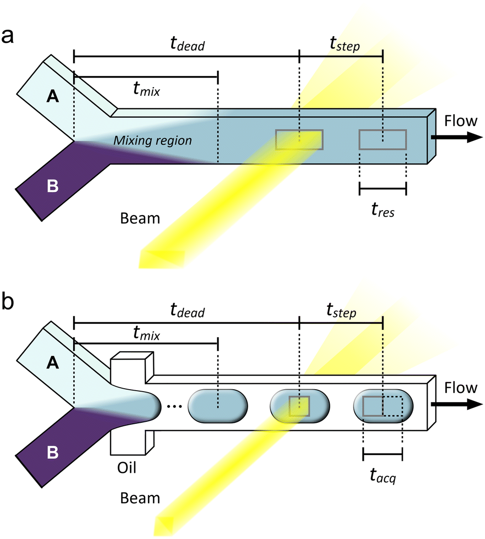 | ||
| Fig. 2 Examples of (a) continuous and (b) droplet microfluidic flow reactors illustrating some important definitions of time related to sample environments for operando X-ray analysis. Reactants A and B are mixed at a Y-junction. Based on a given steady flow rate, the characteristic lengths shown correspond to characteristic times, t. A simple diffusive mixer is shown in (a), but various other designs could be used in the mixing region to accelerate the mixing process, i.e., by exploiting inertial effects for chaotic mixing.98 Mixing lengths are not to scale. | ||
Mixing times are generally determined through numerical simulations and/or flow experiments using a colorimetric or fluorimetric tracer in the place of chemical reactants.99 Due to small measurement uncertainties or uncertainties in the diffusion coefficients of reactant molecules, often the mixing time is reported as a conservative upper limit or even presented simply as the observation dead time (tdead, Fig. 2a). This term is inherited from the stopped-flow community and simply means the time between the initiation of a reaction (t = 0) and the first possible measurement time. This distinction between tmix and tdead stems from the physical separation between the mixing element and the analysis capillary. Depending on the design of a microfluidic device, it may also not be possible to observe the flow right at the point of full mixing, or conversely, a time point after tmix may be targeted intentionally to allow for a factor of safety in the mixing time.
The next important time parameter is the time resolution (tres, Fig. 2a). This term is also defined in different ways in the literature, where it is sometimes taken to be equivalent to the mixing time, tmix. The logic for this definition is that it would be impossible to achieve higher time resolution than the distribution of fluid age resulting from mixing. To some extent this is accurate, however, if mixing is fast, often the limiting factor to resolution is the time it takes for fluid to pass through the beam, i.e., the age distribution of fluid within the beam neglecting mixing time. This is determined by the beam size in the direction of the flow and the fluid velocity, and it is one of several reasons why microfocused X-ray beams are typically utilized for microfluidics experiments. Improving temporal resolution can be a real advantage for the analysis of rapid kinetics, which are not able to be followed with the achievable acquisition times of most current X-ray instrumentation alone. For example, in the case of a microfocused beam (typically ∼20 μm in size) and an average linear velocity of 0.1 m s−1 (corresponding to a flow rate of 1 μL s−1 in a channel with a cross-section of 100 μm × 100 μm), one can obtain a temporal resolution of around 0.2 ms—much shorter than usual acquisition times.
Related to tres is the average time interval between each measurement position, or the time step (tstep, Fig. 2a). Depending on the device design and operation and the position of the X-ray windows, the distance between each measurement position can vary, with the smallest tstep without overlap being the effective length of the beam along the flow channel. This is often considered to be the full-width at half maximum (FWHM) of the beam intensity. If measurement positions are only a beam length apart, then tstep is equal to tres. Such an arrangement provides the highest possible resolution of the reaction taking place along the flow channel, but depending on the reaction kinetics, having many positions so close together may not be useful and will add unnecessary time and complication to an experiment. Importantly, like for tres, tstep is related to only the beam size and the fluid velocity with respect to the beam and is completely independent of the X-ray exposure time and detector frame rate unlike for stopped-flow experiments. There is some uncertainty in the time step arising from the precision of the sample stage motors and Taylor dispersion, i.e., the fact that fluid at the center of the channel will travel faster than fluid near the walls,100 although these effects are not often explicitly considered in operando X-ray experiments.
Alternatively, it is possible to eliminate Taylor dispersion by using a segmented flow of droplets in an immiscible continuous phase, where liquid and solids contained within a droplet stay together along a channel, forming an independent microreactor (Fig. 2b).100 In this case, tres is not defined by the beam size, but rather by the spread of reaction times in the fluid composing a droplet (i.e., tmix), assuming all droplets to be uniformly and continuously mixed. However, when utilizing droplets, an additional sampling consideration must be made to ensure that the signal of interest from the droplets is not masked by noise from the continuous phase.101 In droplet microfluidics, high density fluorinated oils are often utilized in this role, and these scatter significant numbers of photons. Thus, to minimize or eliminate noise from the continuous phase, the data acquisition strategy must adopt a droplet size, droplet velocity, beam size, and frame rate combination such that the effective acquisition length (or acquisition time, tacq) is contained within a single droplet (Fig. 2b).92 This consideration is analogous to the Nyquist rate in analog-to-digital signal conversion.102 For this reason, it is even more important to use a microfocused X-ray beam when performing an experiment with a droplet microfluidic device. Taylor dispersion can also be minimized using hydrodynamic flow focusing to concentrate reactants into a narrow fluid jet. However, this is only effective at short reaction times when diffusion can be neglected103 and also requires a microfocused X-ray beam to isolate data from the concentrated jet.
Now that we have learned about some alternatives to micro- and milli-fluidics and briefly discussed some characteristics and definitions for fluidic sample environments, the following three sections will cover the use of these devices in X-ray scattering & diffraction, spectroscopy, and imaging, respectively. The goal of these sections is to present as comprehensive of a view as possible into the work done in these areas in order to serve as a reference and to present the varied ways researchers have addressed the challenges of performing in situ X-ray measurements. These sections will also contain a greater focus on applications by discussing the science enabled by each device. Thus, to present as clear of a record as possible, the majority of our analysis and perspectives on the field will be included at the end of the review.
3 Devices for X-ray scattering and diffraction
3.1 Brief theory and overview
In microfluidic and millifluidic synchrotron X-ray analysis to date, scattering- and diffraction-based methods have received the most attention. The phenomenon of X-ray scattering results from elastic and inelastic interactions between incoming X-ray photons and the electrons within a sample.104 Focusing on the more common methods that utilize elastic X-ray scattering (of which diffraction is a special case), these provide the user with information on the length-based properties of a sample, such as its structure, size, and shape, depending on the scattering angle at which photons are analyzed.104,105 This dependence is well described by the relation formulated by W. L. Bragg in 1912:λ = 2d![[thin space (1/6-em)]](https://www.rsc.org/images/entities/char_2009.gif) sinθ sinθ | (1) |
This distinction has led to the development of two groups of techniques: those based on X-ray diffraction (XRD) and those based on small-angle X-ray scattering (SAXS). The term “wide-angle X-ray scattering” (WAXS) also appears in the literature and is equivalent to X-ray diffraction. “XRD” is a term used by crystallographers and engineers, especially with crystalline samples that produce sharp Bragg peaks, whereas “WAXS” is preferred by SAXS practitioners, especially with poorly crystalline or amorphous samples. While there are a variety of different experimental setups for performing SAXS and XRD/WAXS analysis, the most obvious difference between the two groups is the position of the detector. Wide angles are analyzed when the detector is close to the sample (normally within ∼5–50 cm), whereas small angles are more easily accessed when the detector is a meter to several meters away or more. By convention, XRD data are typically plotted as a function of 2θ and scattering data as a function of the scattering vector, q = (4π/λ)sin(θ). Micro- and milli-fluidic devices for performing both SAXS and XRD/WAXS analysis are discussed below (Table 1).
| X-ray technique(s) | Device material(s) | Fabrication and/or assembly method | Window material, thickness | Geometry, beam pathlength | Sample(s) investigated | Beamline, source, X-ray energy | Beam size | Acquisition mode, exposure time | Mixing time, tmix | Minimum time step, tstep | Total residence time | Ref. |
|---|---|---|---|---|---|---|---|---|---|---|---|---|
| SAXS | PDMS | Photolithography, soft lithography, cured and plasma-bonded | PDMS, 2 × 19 μm | Transmission, 52 μm | SiO2 NPs | ID13, ESRF, 12.47 keV | 1.5 μm × 1.5 μm | Single-shot, 1 s | N/A | 160 s | N/A | Merlin et al. (2011)106 |
| SAXS | Kel-F, stainless steel, mica | Machining, threaded | Mica, unknown | Transmission, 750 μm | Au NPs with various ligands | BL 11.3.1, ALS, 11 keV | 100 μm spot | Single-shot, 2–5 min | N/A | N/A | 2 ms | McKenzie et al. (2010)107 |
| BL 7.3.3, ALS, 10 keV | 0.24 mm × 1 mm | |||||||||||
| SAXS | PMMA, Kapton | Unknown | Kapton, unknown | Transmission, 1 mm | Ag NPs | BL08B2, SPring-8, 12.4 keV | 230 μm × 370 μm | Single-shot, 100 s | Unknown | 0.18 ms | ∼1–10 s | Takesue et al. (2011)108 |
| SAXS | Device 1: PDMS/glass | Device 1: photolithography, cured and plasma-bonded | Device 1: glass, 10 μm | Device 1: transmission, 0.3–4 mm | Au NPs | 7T-MPW-SAXS, BESSY II, 7.5–8 keV | 50 μm × 300 μm ellipse | Single-shot, 900 s | Device 1: N/A | Device 1: unknown | Device 1: unknown | Stehle et al. (2013)109 |
| Device 2: glass capillaries and slide | Device 2: pipette pulling, epoxy | Device 2: glass, unknown | Device 2: transmission, unknown | Device 2: ∼1 s | Device 2: <0.1 s | Device 2: ∼3–5 s | ||||||
| SAXS | OSTEMER 322, Kapton | Photolithography, soft lithography, cured, cure-bonded | Kapton, 2 × 25 μm | Transmission, 300 μm | Cerium oxalate | SWING, SOLEIL, 12 keV | 80 μm × 150 μm | 200 ms | Unknown | 33.5 ms | ∼6–7 s | Rodríguez-Ruiz et al. (2018)110 |
| SAXS | Unknown | Compression fittings | Capillary of unknown material and wall thickness | Transmission, 2 mm outer diameter capillary | Pd NPs | 1–5, SSRL, 15.5 keV | 500 μm × 500 μm | Unknown | Unknown | N/A | Unknown | Fong et al. (2021)111 |
| SAXS | Titanium, diamond, unknown O-ring material | Machined, clamped | Diamond, 2 × unknown | Transmission, unknown | Supercritical CO2 | 4–2, SSRL, 15 keV | Unknown | Multiframe, 50–60 × 5 s | N/A | N/A | N/A | Younes et al. (2023)112 |
| GISAXS | COC (TOPAS), glass slide | Machined, thermally bonded, clamped | COC, 2 × 500 μm | Reflection, 1 mm channel width, 7.45 mm beam footprint | Au NPs | BW4, DORIS III, 8.98 keV | 65 μm × 35 μm | Single-shot, 60 min | Unknown | N/A | N/A | Moulin et al. (2008)113 |
| GISAXS | COC (TOPAS), polymer-coated glass slide | Machined, thermally bonded, clamped | COC, 2 × 500 μm | Reflection, 1 mm channel width, beam footprint unknown | Au NPs | BW4, DORIS III, 8.98 keV | 30 μm × 60 μm | Single-shot, 200 s | N/A | N/A | N/A | Metwalli et al. (2009)114 |
| GISAXS/GIWAXS | Silicon, glass (Pyrex) | Photolithography, reactive ion etching, anodic bonding | Silicon, 10 μm | Reflection, unknown channel width, 2.9 mm beam footprint | CO oxidation on RuO2 NPs | cSAXS, SLS, 11.2 keV | 10 μm × 100 μm | Unknown | Unknown | N/A | 23 s | Kehres et al. (2016)115 |
| SAXS/WAXS | Glass capillaries, aluminum tube | Pipette pulling, compression fittings | PET (Melinex), 2 × 250 μm | Transmission, 3 mm | 2,6-Dibromo-4-nitroaniline | 16.1, SRS Daresbury, 8.8 keV | Unknown | Single-shot, 30–60 s | 90 ms | 20 ms | ∼1–2 s | Alison et al. (2003)116 |
| XRD | Silicon tube, hastelloy | Machined, clamped | Silicon tube, unknown | Transmission, 1 mm | CaCO3 on silicon | X17B1, NSLS, 67 keV | Unknown | Single-shot, 120 s | Unknown | N/A | Unknown | Chen et al. (2007)117 |
| XRD | Silicon tube, hastelloy | Machined, clamped | Silicon tube, unknown | Transmission, 1 mm | CaCO3 with polymer additive on silicon | X17B1, NSLS, 67 keV | Unknown | Single-shot, 120 s | Unknown | N/A | Unknown | Chen et al. (2009)118 |
| XRD | Stainless steel, hastelloy | Machined, clamped | Stainless steel tube, unknown | Transmission, 2 mm | BaSO4 with polymer additives on stainless steel | X17B1, NSLS, 70 keV | Unknown | Single-shot, 120 s | Unknown | N/A | 0.75 s | Mavredaki et al. (2011)119 |
| GIWAXS | Acetal plastic, Kapton | Machined, clamped | Kapton, 2 × 125 μm | Reflection, 15 mm channel width, 717 μm beam footprint, 55 μm penetration depth | FeCO3 on X65 stainless steel | I15, diamond, 40 keV | 100 μm diameter | Multiframe, 5 × 60 s | Unknown | N/A | Unknown | Burkle et al. (2016)120 |
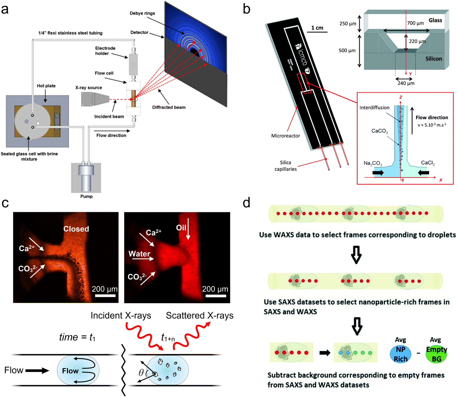
| SAXS/WAXS | Silicon, glass (Pyrex) | Photolithography, wet etching, anodic bonding | Glass, 250 μm, silicon, 280 μm | Transmission, 220 μm | CaCO3 | ID02, ESRF, 12.49 keV | 50 μm × 50 μm | Single-shot, 200 ms | Unknown | N/A | Unknown | Beuvier et al. (2015)121 |
| Powder XRD | PMMA, PTFE, Kapton, silicone | UV laser cutting, clamped | Kapton, 2 × 75 μm | Transmission, 300 μm | CaCO3 with nucleating agents | ID13, ESRF, 13 keV | 12 μm × 15 μm | Multiframe, 1000 × 20 ms | ∼1 s | 4 s | 140 s | Levenstein et al. (2020)102 |
| I11, diamond, 15 keV | 200 μm × 200 μm | Single-shot, 60–120 s | ∼10 s | 9 s | 325 s | |||||||
| Powder XRD | PMMA, PTFE, Kapton, silicone | UV laser cutting, clamped | Kapton, 2 × 75 μm | Transmission, 300 μm | CaCO3 with nucleating agents, Au NPs, iron oxide NPs | ID13, ESRF, 13 keV | 12 μm × 15 μm | Multiframe, 1000 × 20 ms | ∼1 s | 4 s | 140 s | Levenstein et al. (2019)122 |
| I22, diamond, 12.4 keV | 80 μm × 320 μm | Multiframe, 2000 × 10 ms | ||||||||||
| Powder XRD | FEP, PTFE, Kapton tubes | Custom machined fittings, silicone sealant, tubing coiling | Kapton tube, 95 μm wall | Transmission, 3.19 mm | Urea: barbituric acid, carbamazepine | I11, diamond, 15 keV | 1 mm × 1 mm | Multiframe, 51 × 100 ms | Unknown | 138–230 s | 10.4–19.3 min | Levenstein, Wayment et al. (2020)123 |
| SAXS and WAXS | OSTEMER 322 | Photolithography, soft lithography, cured and laminated | OSTEMER 322, 2 × 200 μm | Transmission, 150 μm | Au NPs, cerium oxalate | SWING, SOLEIL, 12 and 16 keV | 50 μm × 125 μm | Multiframe, 100 × 50 ms | ∼0.5 s | 6 ms | 30 s | Lange et al. (2020)92 |
| SAXS/WAXS | PDMS/glass | Photolithography, soft lithography, cured and plasma-bonded | Fused silica/Kapton tube, 50 μm wall | Transmission, 250 μm | Iron oxide NPs | I22, diamond, 12.4 keV | 40 μm × 40 μm | Multiframe, 1000 × 20 ms | ∼1 s | 20 s | 130 s | Radajewski et al. (2021)124 |
| Single-crystal XRD | Custom formulated RLV-1 resin | 3D printing (DLP) | 3D-printed resin, 1.3 mm | Transmission, ∼100–250 μm | CaSO4·2H2O, protein crystals | ID30-A3, ESRF, 12.82 keV | 30 μm × 50 μm | Unknown | ∼1.5 s | N/A | N/A | van der Linden et al. (2020)125 |
| ID30-B, ESRF, 12.41 keV | 10 μm × 10 μm | Unknown | ||||||||||
| SAXS and WAXS | Glass capillary, PTFE tubing, polymer fittings | Tube crimping, compression fittings, heat-shrink tubing | Borosilicate capillary, 50 μm wall | Transmission, 2 mm | YVO4:Eu NPs | SWING, SOLEIL, 15 keV | 375 μm × 75 μm | Multiframe, 10 ms frames for SAXS and 0.1 or 2 s frames for WAXS | ∼250 ms | N/A | 400 ms (longer using stopped flow and peristaltic pump) | Fleury et al. (2014)126 |
| Powder XRD | Glass capillary, PTFE tubing, polymer fittings | Compression fittings, tubing coiling | Quartz capillary, 200 μm wall | Transmission, 1 mm | Iron oxide NPs | XRD1, Elettra, 12.4 keV | Unknown | Single-shot, 10 min | ∼50 ms | N/A | 5–160 s (longer using semi-batch setup) | Besenhard et al. (2020)127 |
| SAXS and WAXS | Glass capillary, PTFE tubing, polymer fittings | Tube crimping, compression fittings, heat-shrink tubing | Borosilicate capillary, 50 μm wall | Transmission, 1.5 mm | Cerium oxalate | SWING, SOLEIL, 16 keV | 375 μm × 75 μm | Multiframe, 20 × 1 s for SAXS and 20 × 4 s for WAXS | ∼250 ms | N/A | 250 ms (longer using stopped flow) | Durelle et al. (2023)128 |
| Total scattering/PDF | Kapton tube, metal fittings | Compression fittings | Kapton tube, unknown | Transmission, 2 mm | ZIF-8 | 28-ID-2, NSLS-II, 67.86 keV | Unknown | “Rapid acquisition mode”, ∼1–10 s | Unknown | N/A | 0.05–2 s | Terban et al. (2018)129 |
| Total scattering/PDF | Glass capillary, Kapton tube, stainless steel fittings | Compression fittings, 3D-printed adapters | Glass capillary, 100 μm wall | Transmission, 1.3 mm or 0.9 mm | Al3+, FeS | 11-ID-B, APS, 58.62 keV | 0.5 mm × 0.5 mm | Single-shot, 1, 10, and 100 s | ≤0.1 s | 0.01–0.1 s | 0.1–10 s | Beauvais et al. (2021)130 |
| 28-ID-1, NSLS-II, 74.46 keV | Beauvais et al. (2022)131 | |||||||||||
| Total scattering/PDF | Carbon fiber capillary, polyethylene, rubber tubing | Compression fittings | Epoxy-aligned carbon fiber capillary, 0.67 mm | Transmission, 1.83 mm | Pt NP-coated CNTs and graphene, Fe–Ni layered double hydroxide NPs, LiCoO2 | 11-ID-B, APS, 58.65 keV | Unknown | Unknown | N/A | N/A | N/A | Young et al. (2017)132 |
| 11-ID-C, APS, 105 keV | ||||||||||||
| 6-ID-D, APS, 100 keV | ||||||||||||
| Total scattering/PDF and GIWAXS | Kapton, VeroClear-RGD810 resin, porous glass array, electrode materials | Epoxy, atomic layer deposition of electrodes, compression fittings | Kapton, 2 × 25 μm | Transmission, 2.4 mm | Amorphous cobalt oxide thin films | 11-ID-B, APS, 58.7 keV | 300 μm × 500 μm | Single-shot, 2–5 min | N/A | N/A | N/A | Kwon et al. (2019)133 |
| 6-ID-D, APS, 100.3 keV | 300 μm × 500 μm | |||||||||||
| 11-ID-D, APS, 23 keV | 15 μm vertical |
3.2 SAXS
Around the same period, several millifluidic studies were also performed. McKenzie et al. designed a custom flow-cell to enable simultaneous in situ SAXS and ultraviolet-visible (UV-vis) spectroscopy and validated it by determining the size distribution of pre-made suspensions of reference Au NPs (Fig. 3a).107 The ability to perform both in situ and ex situ UV-vis allowed for quality control and the comparison of in situ SAXS data to subsequent ex situ transmission electron microscopy (TEM) of the different Au NP standards after surface-deposition, which would be especially important when characterizing experimental samples. Takesue et al. performed operando SAXS analysis of Ag NP synthesis using a poly(methyl methacrylate) (PMMA) device with Kapton X-ray windows (Fig. 3b).108 By utilizing a very high flow rate (120 mL min−1), the authors obtained a turbulent flow, which facilitated rapid mixing of reactants and also sub-ms time resolution through the vertical movement of the device in the beam. In this case, the continuous flow of solution permitted long X-ray exposures (>1 min) at each channel position to obtain good scattering statistics of dilute intermediate species without sacrificing time resolution.
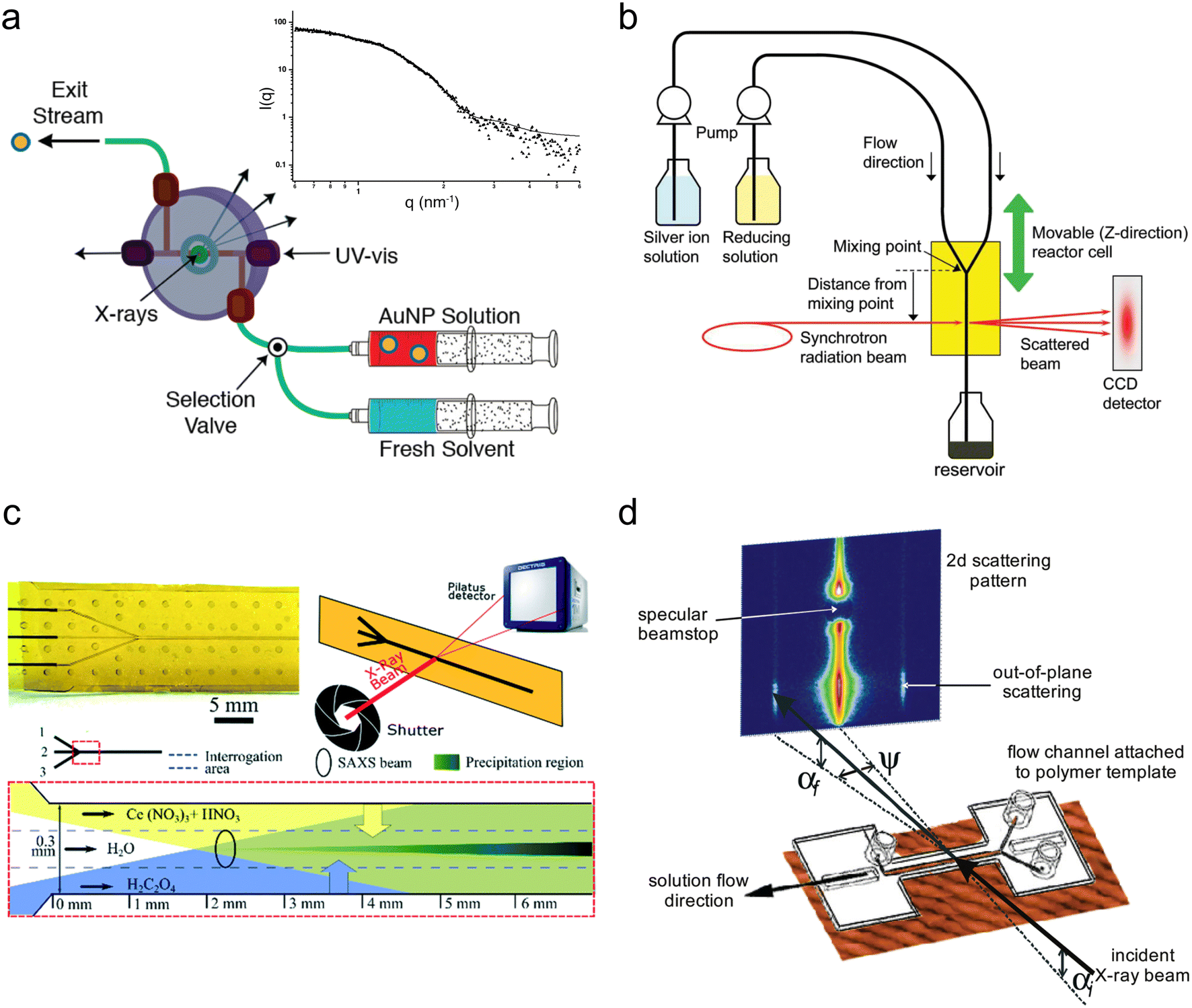 | ||
| Fig. 3 Devices for SAXS analysis. (a) Millifluidic flow-cell for simultaneous SAXS and UV-vis of nanoparticle solutions. Inset: Example 1D scattering pattern of AuNP suspension (adapted with permission from McKenzie et al., 2010; Copyright 2010 American Chemical Society)107 (b) Experimental setup for sub-ms synchrotron SAXS measurements of the early stages of AgNP synthesis (reprinted with permission from Takesue et al., 2011; Copyright 2011 American Chemical Society).108 (c) Continuous flow microfluidic device for the study of cerium oxalate precipitation (top left: photo of the device; top right: measurement geometry; bottom: illustration of the mixing configuration with the water buffer flow; adapted with permission from Rodríguez-Ruiz et al. 2018; Royal Society of Chemistry).110 (d) Example of a microfluidic GISAXS experiment (reprinted with permission from Metwalli et al., 2009; Copyright 2009 American Chemical Society).114 | ||
Another method for limiting precipitation on channel walls without producing droplets is by introducing a strong ‘buffer’ flow of water between reactant streams. This delays their contact and slows down their mixing to prevent a sudden precipitation event that could instantly clog a device. Such a method was employed by Rodríguez-Ruiz et al. in an OSTEMER-Kapton microfluidic device to study the precipitation of the highly insoluble, rare earth mineral, cerium oxalate (Fig. 3c).110 Using a flow of water >10 times faster than their reactant flows (also resulting in a >10 times reactant dilution), they were able to successfully acquire scattering curves from within the first second of the reaction. However, the slowed mixing resulting from the water flow meant that it was not possible to analyze reaction times <0.2 s due to inconsistent background signal.
3.3 XRD/WAXS
 | ||
| Fig. 4 Devices for WAXS/XRD analysis. (a) An experimental setup for millifluidic GIWAXS and electrochemical measurement of steel corrosion (reprinted from Burkle et al. 2016 with the permission of AIP Publishing).120 (b) A hybrid silicon-glass microfluidic device for continuous flow study of CaCO3 crystallization (reprinted with permission from Beuvier et al. 2015; Royal Society of Chemistry).121 (c) Comparison of CaCO3 crystallization in microfluidic devices in continuous flow (top left) versus under conditions optimized to prevent scaling (top right). An illustration of the distance-to-time conversion enabled when scaling is prevented (bottom) (adapted with permission from Levenstein et al., 2020; Royal Society of Chemistry).102 (d) A workflow for SAXS/WAXS frame selection and background subtraction for droplet microfluidics (reprinted with permission from Radajewski et al., 2021; Royal Society of Chemistry).124 | ||
In order to isolate scattering from the droplets from that of the surrounding fluorinated oil phase, the authors implemented a multiframe data acquisition and processing approach first used for bioSAXS.101 Briefly, short 20 ms frames were captured at a rate of 50 Hz and WAXS frames containing the characteristic scattering of the oil phase were identified and discarded. The remaining frames were then summed to obtain a good signal-to-noise ratio at each position.122 This WAXS-based technique was later implemented in a millifluidic flow system,123 and a similar technique was also performed by Lange et al., who utilized SAXS frames to distinguish between the water and oil phases.92 More recently, Radajewski et al. presented an innovative data processing technique combining both WAXS and SAXS frame selection to isolate not only droplets, but also the sections of droplets with the highest concentration of sample for subsequent data treatment (Fig. 4d).124 Alternatively, for studies not requiring operando measurements, van der Linden et al. developed a 3D-printed device for storing and measuring samples contained with isolated, static droplets to avoid signal from the oil phase.125
 | ||
| Fig. 5 Simple ‘plug-and-play’ millifluidic devices for XRD/WAXS/PDF analysis. (a) A setup for in situ SAXS/WAXS utilizing commercial mixers and custom temperature-controlled sections for time-delay (reprinted from Besenhard et al., 2020; with permission from Elsevier).127 (b) A Norby-style device with active mixing for X-ray PDF analysis (adapted with permission from Beauvais et al. 2022; IUCr).131 | ||
3.4 Total scattering/PDF
In this final scattering section, we will cover recent efforts in millifluidic X-ray total scattering, used for performing pair distribution function (PDF) analysis of atomic to nanoscale correlations within materials. These measurements are usually performed at high energy beamlines to incorporate scattering from small length scales since wavelength and energy are inversely proportional and wavelength and the probed length scale are directly proportional at fixed θ (see eqn (1)). By utilizing crystalline Bragg diffraction and diffuse scattering at large angles normally neglected during XRD analysis (i.e., the “total” scattering pattern), the PDF technique provides information on not only long-range crystalline order within a sample, but also short-range correlations within even amorphous materials.144 These techniques are additionally well suited for in situ analysis because the high energies impart more penetration power and allow the use of thicker and denser samples and sample environments.Terban et al. performed in situ X-ray PDF analysis of the synthesis of the zeolitic imidazolate framework, ZIF-8,129 using a simple millifluidic continuous flow device consisting of a Kapton tube, a metallic frame and commercial fittings mounted on a goniometer head in the same way as a Norby cell. With this setup, they were able observe the formation of long-lived solution species and amorphous solid phases during the synthesis of this model metal–organic framework. Similarly, Beauvais et al. developed a millifluidic device resembling a Norby design but comprising an active vibration mixing element (Fig. 5b).131 They tested a variety of injection capillary sizes, types and materials, including glass and Kapton, and converged on a design that fully mixed reactants in less than a few hundred milliseconds. The authors validated the system by studying the hydrolysis of Al3+ and then went on to study the formation of FeS by a ligand-exchange reaction, demonstrating the presence of previously unknown intermediate phases in the form of nanosheets.130
A few groups have also developed innovative cells that enable in situ X-ray PDF measurements of electrochemical processes. For example, Young et al. designed a millifluidic electrochemical cell with an epoxy-aligned carbon fiber capillary serving as both the working electrode and the X-ray window.132 A recirculating flow of electrolyte solution could be applied through the capillary, and various samples relevant to electrocatalysis and batteries could be loaded and measured during cycling, including Pt nanoparticle-coated carbon nanotubes and LiCoO2 powder. Kwon et al. developed their own electrochemical cell consisting of a 3D porous glass capillary-array (GCA) sitting in an electrolyte reservoir with Kapton walls to facilitate X-ray analysis.133 The GCA array was coated by gold and either indium tin oxide (ITO) or indium zinc oxide (IZO) to serve as the working electrode, and fresh electrolyte was pumped through the GCA pores from below the reservoir using a syringe pump during cycling.
4 Devices for X-ray spectroscopy
4.1 Brief theory and overview
X-ray spectroscopy techniques are utilized to obtain chemical information such as elemental composition, oxidation state, and coordination number. This section will be focused primarily on X-ray absorption spectroscopy (XAS), which is one of the main groups of X-ray spectroscopic techniques and the one utilized in most previous micro- and milli-fluidic studies. Another major type of X-ray spectroscopy is X-ray photoelectron spectroscopy (XPS), but to our knowledge, in situ XPS has been performed exclusively in free liquid jets,145 likely due to the poor transmission of electrons exiting through device windows. There are two primary acquisition modes for XAS analysis: transmission and fluorescence. The most common, transmission XAS, is based on measuring the incident beam flux (I0) and the flux of the beam transmitted through the sample (I), which are related by the Beer–Lambert law:| I = I0·e−μ(λ)x | (2) |
XAS is performed in fluorescence mode by monitoring the total yield of secondary X-rays at 90° from the incident beam (normally 45° from the sample) rather than the transmitted flux, which is helpful when using thick or highly dilute samples.146,147 For both modes, different acquisition strategies using polychromatic radiation and position/energy-resolved detectors can also be employed to more rapidly record full spectra without scanning the energy of the incident beam.148–150 The closely related technique of X-ray fluorescence (XRF) has also been performed with microfluidic devices,151,152 although primarily for 2D elemental mapping and laboratory analysis, and will thus be covered in sections 5 and 6, respectively. Further details on the micro- and milli-fluidic devices for X-ray spectroscopy discussed below can be found in Table 2.
| X-ray technique(s) | Device material(s) | Fabrication and/or assembly method | Window material, thickness | Mode, beam pathlength | Sample(s) investigated | Beamline, source, X-ray energy | Beam size | Acquisition mode, exposure time | Mixing time, tmix | Minimum time step, tstep | Total residence time | Ref. |
|---|---|---|---|---|---|---|---|---|---|---|---|---|
| XRF | Fused silica capillary, polyethylene tubing | Interference fit | Polyethylene, 193 μm wall | Fluorescence, 580 μm | Co, Cu, and Zn solutions | X-26A, NSLS, 10 keV | 30 μm × 40 μm | Multiframe, 1 s exposure, 0.25 Hz | N/A | N/A | N/A | Ringo et al. (1999)151 |
| XRF | Fused silica capillary, polyethylene tubing | Interference fit | Polyethylene, 355 μm wall | Fluorescence, 380 μm | Fe, Co, Cu, and Zn solutions | X-26A, NSLS, 10 keV | 40 μm × 40 μm | Multiframe, 1 s exposure | N/A | N/A | N/A | Mann et al. (2000)152 |
| XANES and EXAFS | Ti-6Al-4V alloy, Pt/Ir alloy, diamond (type 1B) | Machining, press fit, clamping | Diamond, 2 × 1 mm | Transmission, ∼1–100 mm | Tungstate solutions | ID-20, APS, W L3-edge (10.21 keV) | 1.5 mm diameter | Unknown | N/A | N/A | N/A | Hoffmann et al. (2000)153 |
| Diamond, 2 × 250 μm | Transmission, ∼2.5 mm | Chromate solutions | X-19A, NSLS, W L3-edge (10.21 keV) | 2 mm diameter | Hoffmann et al. (2001)154 | |||||||
| ID-20, APS, Cr K-edge (5.99 keV) | Unknown | |||||||||||
| XANES and EXAFS | Silicon, glass | Deep reactive ion etching, anodic bonding | Silicon, unknown | Fluorescence, ≥250 μm | Dehydrogenation of methanol on Ag | 16.5, SRS Daresbury, Ag K-edge (25.5 keV) | 0.4 mm × 10 mm | Single-shot, 40 min | N/A | N/A | ∼10 ms gas dwell time | Sankar et al. (2007)155 |
| XANES and μXRF | Silicon, glass, silicon nitride, SU-8 | Photolithography, wet etching, reactive ion etching, anodic bonding | Silicon nitride, 1 μm, SU-8, 1 μm | Fluorescence, 570 μm | CdSe → Ag2Se nanocrystals | 10.3.2, ALS, Se K-edge (12.66 keV) | 16 μm × 7 μm | Multiframe, 4 × >100 s | ∼14 ms | ∼8–16 ms | ∼50–100 ms | Chan et al. (2007)156 |
| XANES | Silicon, glass | Deep reactive ion etching, fusion bonding | Silicon, 300 μm, glass, 200 μm | Fluorescence, ≥300 μm | Au NPs | P06, Petra III, Au L3-edge (11.92 keV) | Unknown | Unknown | <1 ms | ∼1 μs | 20 ms | Hofmann et al. (2016)157 |
| XANES | Silicon, glass | Deep reactive ion etching, fusion bonding | Silicon, 300 μm, glass, 200 μm | Fluorescence, ≥300 μm | Au NPs | SuperXAS, SLS, Au L3-edge (11.92 keV) | 150 μm × 100 μm | Single-shot, 4 min | <2 ms | ∼1 μs | 20 ms | Tofighi et al. (2017)158 |
| XANES and EXAFS | Silicon, borosilicate glass | Deep reactive ion etching, anodic bonding | Glass, 2 × 175 μm | Transmission and fluorescence, 742 μm | Fe, Br, and Pb salt solutions | Balder, MAX IV, Fe K-edge (7.11 keV), Pb L3-edge (13.04 keV), Br K-edge (13.47 keV) | 50 μm × 50 μm | Multiframe, 10 × 100 s for EXAFS and 4–6 × 25 s for XANES | N/A | N/A | N/A | Micheal Raj et al. (2021)159 |
| XANES/EXAFS | Unknown | Unknown | Unknown | Fluorescence, unknown | Pt NPs | I18, diamond, Pt L3-edge (11.56 keV) | 400 μm × ∼250 μm | Unknown | Unknown | Unknown | 37.3 min | Britto et al. (2023)160 |
| XANES | PMMA | Hot embossing | PMMA, unknown | Fluorescence, ≥500 μm | Co NPs | XMP, CAMD, Co K-edge (7.78 keV) | 50 μm × 80 μm | Single-shot, 5–7.5 min | Unknown | ∼2 ms | 50 s | Zinoveva et al. (2007)161 |
| XANES and EXAFS | Unknown | Unknown | Kapton, unknown | Fluorescence, ≥500 μm | CdSe NPs | BL13B1, PF, 12.6–12.7 keV | 1 mm × 0.5 mm | Unknown | Unknown | 47–118 ms | 30 s | Oyanagi et al. (2011)162 |
| NW2, PF-AR, 12.6–12.7 keV | ||||||||||||
| XANES and EXAFS | PVC, brass, graphite | Machining, clamping, pressure fittings, conductive epoxy | Kapton, unknown, graphite, 500 μm | Transmission, ∼400 μm (∼200 μm electrolyte and ∼200 μm sample) | Iron and iron oxide phases | ID24, ESRF, Fe K-edge (7.11 keV) | 50 μm × 100 μm | Multiframe, ms exposures | N/A | N/A | Unknown | Monnier et al. (2008)163 |
| Fluorescence, 282 μm | BM30b, ESRF, Fe K-edge (7.11 keV) | 30 μm × 150 μm | Multiframe, 7 min for XANES, and 3 × 30 min for XANES + EXAFS | Monnier et al. (2014)164 | ||||||||
| DIFFABS, SOLEIL, K-edge (7.11 keV) | 300 μm × 300 μm | Multiframe, unknown | ||||||||||
| XANES and EXAFS | PET | Commercially purchased | PET, unknown | Fluorescence, ≥150 μm | Au nanostructures | 10-ID, APS, Au L3-edge (11.92 keV) | 50 μm × 50 μm | Unknown | Unknown | 5.4 ms (neglecting mixing time) | ∼25 s | Krishna et al. (2013)165 |
| WDCM, CAMD, Au L3-edge (11.92 keV) | ||||||||||||
| XANES and EXAFS | PETG filament | 3D printing (FDM) | 3D-printed polymer, unknown | Transmission, 80 mm | Pd NPs | STM, Kurchatov, Pd K-edge (24.35 keV) | 0.7 mm × 0.7 mm | Single-shot, 10 min | Unknown | ∼2.7 min | ∼17.6 min | Dobrovolskaya et al. (2023)166 |
| EXAFS | Ti-6Al-4V alloy, diamond (type IIa) | Machining, epoxy, clamping, Poulter seal | Diamond, 2 × 25 μm | Transmission, 150 μm | CaCl2 solution | 20-BM, APS, Ca K-edge (4.04 keV) | 200 μm × 180 μm | Multiframe, 3 × 20 min | N/A | N/A | ∼15 min | Fulton et al. (2004)167 |
| XAS and XES | PTFE, silicon, viton O-ring | Machined, clamped | Silicon nitride, 100 nm silicon carbide, 150 nm | Fluorescence, ≥500 μm | H2O, D2O | 8.0.1, ALS, 550 eV | Unknown | Unknown | N/A | N/A | Unknown | Fuchs et al. (2008)168 |
| XANES | Silicon, PTFE, unknown O-ring and housing material | Machined, clamped | Silicon nitride, 2 × 100 nm | Transmission, 100–800 nm | Water | BL3U, UVSOR-II O K-edge (532 eV) | 200 μm × 200 μm | Single-shot, ∼13 min | N/A | N/A | ∼1 s | Nagasaka et al. (2010)169 |
| XANES | Silicon, stainless steel, gold, unknown O-ring material | Machined, clamped | Silicon nitride, 2 × 100 nm | Transmission, 250 nm | Water, CoCl2 solution, methanol–water mixture | PM3, BESSY II, O K-edge (532 eV) and Co L3-edge (778.6 eV) | 100 μm diameter | Unknown | N/A | N/A | Unknown | Schreck et al. (2011)170 |
| XANES and μXRF | Silicon, PDMS | Wet etching, photolithography, soft lithography, plasma bonding | Silicon nitride, 450 nm | Fluorescence, 57 μm | CaCO3 | Phoenix, SLS, Ca K-edge (4.04 keV) | 50 μm × 75 μm | Multiframe, 10–15 × 8 min | <10 ms | ∼1 ms | ∼5 s | Probst et al. (2021)171 |
| XANES and μXRF | Silicon, PDMS or glass | Wet etching, deep reactive ion etching, photolithography, soft lithography, plasma bonding | Silicon nitride, 120 nm | Fluorescence, 127 μm | Ca2+ ions and EDTA | Phoenix, SLS, Ca K-edge (4.04 keV) | 3 μm × 3 μm | Multiframe, ∼100 min total | <2 ms | 0.365 ms | 2.7 s | Brenker et al. (2022)172 |
| XANES/EXAFS | Stainless steel, graphite, quartz wool | Machined, clamped | Graphite, 300 μm CaF2/glue, 300 μm | Transmission, 2 mm | Pt/Al2O3 catalyst | SuperSAXS, SLS, Pt L3-edge (11.56 keV) | 100 μm × 100 μm | Single-shot, 1 s | N/A | N/A | ∼5 s | Chiarello et al. (2014)173 |
| XANES/EXAFS | Aluminum, CaF2 | Machined, pressure fittings | Al, 2 × 250 μm | Transmission, 5 mm | Pd/Al2O3 catalyst | ID12-EDE, diamond, Pd K-edge (24.35 keV) | 500 μm × 150 μm | Multiframe, 200 × 4.8 ms for EXAFS, single-shot 4.8 ms for XANES | N/A | N/A | Unknown | Dann et al. (2019)174 |
| XANES/EXAFS | Silicon, glass | Photolithography, deep reactive ion etching, anodic bonding | Si, 2 × 250 μm | Transmission, 3 mm | Pd/Al2O3 catalyst | B18, diamond, Pd K-edge (24.35 keV) | 200 μm × 100 μm | Single-shot, 180 s | N/A | N/A | Unknown | Venezia et al. (2020)175 |
| XANES and XES | Fused silica, Kapton | Laser-selective wet etching | Kapton tube, 27 μm wall thickness | Fluorescence, 510 μm | Ferricyanide and ascorbic acid | 6-2b, SSRL, Fe K-edge (7.11 keV) | 418 μm horizontal | Single-shot, 45 min | <1 ms | <1 ms | 157 ms | Huyke et al. (2021)176 |
| XANES/EXAFS and SAXS | Silicon, glass (Pyrex) | Photolithography, deep reactive ion etching, anodic bonding | XAS: silicon, ∼50 μm | XAS: fluorescence, ∼382 μm | Pb NPs | XAS: X18B, NSLS, and 10-ID-B, APS, Pd K-edge (24.35 keV) | XAS: X18B, 0.2 mm × 3 mm, 10-ID-B, 0.5 mm × 0.5 mm | Multiframe, 5 × 20 min | Unknown | 30 s | 95 min | Karim et al. (2015)177 |
| SAXS: silicon, ∼50 μm + second layer of unknown thickness | SAXS: transmission, ∼270 μm | SAXS: 12-ID-C, APS, 18 keV and 12-ID-B, APS, 12 keV | SAXS: unknown | |||||||||
| XANES/EXAFS and anomalous SAXS | PEEK, Kapton (gold-coated) | Machined, clamped | Kapton, 2 × 50 μm | Transmission, 10–50 μm of catalyst, 2 mm of electrolyte | Pt/IrO2–TiO2 electrocatalyst, HClO4 electrolyte | XAS: SuperXAS, SLS, Ir L3-edge (11.22 keV) | XAS: 100 μm × 100 μm | XAS: multiframe, 120 × 500 ms | N/A | N/A | N/A | Binninger et al. (2016)178 |
| SAXS: cSAXS, SLS, four energies near the Pt L3-edge (11.56 keV) | SAXS: unknown | SAXS: unknown | ||||||||||
| XANES and SAXS | OSTEMER 322, Kapton | Photolithography, PDMS injection molding, cured, cure-bonded | Kapton, 2 × 75 μm | XANES: transmission, 1.9 mm | Au NPs | XAS: SuperXAS, SLS, Au L3-edge (11.92 keV) | XAS: 20 μm × 20 μm | XAS: unknown | <0.3 ms | ∼100 ms | XAS: 30 s | Ramamoorthy et al. (2024)179 |
| SAXS: transmission, 370 μm | SAXS: cSAXS, SLS, 11.5 keV | SAXS: 20 μm × 50 μm | SAXS: unknown | SAXS: 0.3 s | ||||||||
| XPCS | Aluminum, Kapton | Machining, clamping | Kapton, 2 × unknown | Transmission, 1 mm | Latex NPs | ID10A, ESRF, 8 keV | 10 μm × 10 μm | Unknown | N/A | N/A | N/A | Busch et al. (2008)180 |
| XPCS | Quartz capillary tube | Compression fittings | Quartz capillary, unknown wall thickness | Transmission, 0.98 mm | PMMA NPs | ID10A, ESRF, 8 keV | 10 μm × 10 μm | Unknown | N/A | N/A | N/A | Fluerasu et al. (2008)181 |
| XPCS | Kapton tube | Compression fittings | Kapton tube, 100 μm wall | Transmission, 1.32 mm | SiO2 NPs | ID10A, ESRF, 8 keV | 10 μm × 10 μm | Unknown | N/A | N/A | N/A | Fluerasu et al. (2010)182 |
| XPCS | NOA 81, polystyrene | Photolithography, soft lithography, UV-curing, cure-bonding | Polystyrene, 2 × 50 μm | Transmission, 200 μm | SiO2 NPs | P10, Petra III, 8.05 keV | 5 μm × 5 μm | Multiframe, 5000 × 3.33 ms | N/A | N/A | N/A | Urbani et al. (2016)183 |
| Heterodyne XPCS | Copper, Kapton | Machining, epoxy, clamping | Kapton, 2 × unknown | Transmission, 0.69 or 0.8 mm | SiO2 NPs | 8-ID-I, APS, unknown | 5 μm × 20 μm | Multiframe, unknown × 1.25 or 16.67 ms | N/A | N/A | N/A | Lhermitte et al. (2017)184 |
| Heterodyne XPCS and XAM | PEEK, stainless steel | Compression fittings, epoxy | PEEK, 2 × 2 mm | Transmission, 1 mm | Li/PEO–LiTFSI/Li battery cell | 8-ID-I, APS, 11 keV | 15 μm × 15 μm | Multiframe, 6000 × 60 ms | N/A | N/A | N/A | Steinrück et al. (2020)185 |
| ID10, ESRF, 8.1 keV | 10 μm × 15 μm | Unknown | ||||||||||
| sp-XPCS, XPXP, SAXS, WAXS | Ti-6Al-4V alloy, diamond (type IIa) | Machining, epoxy, clamping, Poulter seal | Diamond, 2 × 100 μm | Transmission, ∼0.4–1 mm | Supercritical H2O | sp-XPCS: LCLS, 9.5 keV | sp-XPCS: 3 μm diameter | sp-XPCS: multiframe, 105 × 8.33 ms | N/A | N/A | N/A | Muhunthan et al. (2024)186 |
| XPXP: SACLA, unknown | XPXP: unknown | XPXP: unknown | ||||||||||
| SAXS: BL4-2, SSRL, 15 keV | SAXS: unknown | SAXS: unknown |
4.2 XAS
Chan et al. also utilized a silicon-glass microfluidic device to monitor a cation exchange reaction in semiconducting CdSe nanocrystals by XANES at the Se K-edge (12.66 keV).156 In addition to silicon and glass, their device comprised a 2 μm thick silicon nitride/SU-8 X-ray window designed for performing measurements in fluorescence mode (Fig. 6a). In their experiment, a suspension of CdSe nanocrystals was introduced in a hydrodynamic flow focusing geometry surrounded by a sheath flow of Ag+ ions. As the ions diffused into the stream of nanocrystals, the kinetics of the CdSe → Ag2Se transformation could be followed over ∼100 ms with ∼8 ms time resolution owing to the narrow channel width, fast flow rates, and use of a microfocused X-ray beam. Similarly, Hofmann et al.157 and Tofighi et al.158 used a silicon-glass microfluidic device to study the synthesis of Au nanoparticles by fluorescence-based XANES at the Au L3-edge (11.92 keV). By utilizing on-chip turbulent cyclone mixers with <2 ms mixing time, the authors were able to gain access to early stages of the synthesis after only 1–2 ms of dead time.
 | ||
| Fig. 6 Devices for hard XAS analysis. (a) Design of a microfluidic device with a silicon nitride window for XAS in fluorescence mode (adapted with permission from Chan et al., 2007; Copyright 2007 American Chemical Society).156 (b) Br K-edge XANES spectra of aqueous NaBr solutions at the indicated molar concentrations. The dark grey curves are from transmission detection and the green curves are from fluorescence detection (adapted with permission from Micheal Raj et al., 2021; Royal Society of Chemistry).159 (c) Design of a 3D-printed millifluidic device for XAS in transmission mode (adapted with permission from Dobrovolskaya et al., 2023; Copyright 2023 American Chemical Society).166 | ||
More recently, Micheal Raj et al. reported a silicon-glass type microfluidic device for performing both fluorescence and transmission mode XANES and EXAFS.159 They validated their device by studying Fe, Pb, and Br salt solutions and evaluating the quality of fluorescence vs. transmission mode data collected at different ionic concentrations between 1 mM and 1 M (Fig. 6b). Good quality data were obtained for Pb and Br solutions at the Pb L3-edge (13.04 keV) and Br K-edge (13.47 keV), however, the thick glass windows of the device (∼500 μm) resulted in strong attenuation at the Fe K-edge (7.11 keV), preventing further analysis. For Pb and Br, fluorescence detection performed better at concentrations of 1 mM, transmission better at 1 M, and both performed similarly at intermediate concentrations. The authors also paid particular attention to the world-to-chip connections of their device by designing a 3D-printed sample holder that enabled reproducible and safe mounting at the beamline. Britto et al. used a commercial microfluidic device for an operando XANES/EXAFS study of the synthesis of Pt NPs in fluorescence mode.160 Their device had a long channel length, and by tuning the flow rates, the authors were able to study the synthesis over reaction times from a few seconds to almost 40 minutes. Using multivariate analysis of the data, they were able to identify two intermediate phases that formed during the conversion of the H2PtCl6 precursor into metallic Pt.
Several polymer-based microfluidic devices have also been reported for XAS analysis at hard X-ray energies. For example, Zinoveva et al. utilized a PMMA microfluidic chip to study the synthesis of Co nanoparticles by fluorescence mode XANES at the Co K-edge (7.78 keV).161 Similarly, Oyanagi et al. studied the nucleation and growth of CdSe nanoparticles using fluorescence mode XANES and EXAFS at the Se K-edge.162 Their device consisted of two components: a microfluidic continuous flow mixer and a separate module comprising a Kapton capillary tube and a resistive heating element for studying reactions under high temperatures. Here, the combination of XANES and EXAFS enabled the modeling of the XANES data with multi-scattering calculations and comparison to EXAFS data in order to estimate the kinetics of Se–Cd bond formation. Monnier et al. developed a microfluidic electrochemical cell made from polyvinyl chloride (PVC) and brass for operando analysis of the reduction and oxidation of different iron-containing phases.163,164 They performed XANES and EXAFS at the Fe K-edge using both transmission and fluorescence read-out in order to study the corrosion of archeological samples and materials for the storage of nuclear waste.
More recently, Probst et al. utilized a PDMS-based droplet microfluidic device with a SixNy window to study the crystallization of CaCO3.171 They monitored the precipitation of amorphous calcium carbonation (ACC) over the first few seconds of the reaction by fluorescent XANES at the Ca K-edge (4.04 keV). However, owing to the background from the oil phase and the small droplet volumes, long scan times were required at each device position to obtain good photon counting statistics (>1 h). Additionally, the tender incident X-rays produced discolorations in the PDMS layer of the device, although the device shape and flow behavior were unaffected. Similarly, Brenker et al. utilized PDMS- and silicon-based droplet microfluidic devices with SixNy windows for fluorescence mode XANES at the Ca K-edge and found that the silicon devices were more resilient to the incident beam.172 The authors also used the Ca Kα line fluorescence yield to distinguish between droplets and the oil phase and isolate spectra from droplets. Despite this, the low total fluorescence yield still required the averaging of several long scans to obtain a good signal-to-noise ratio (>1 h), which demands highly stable device operation over long durations and large sample volumes.
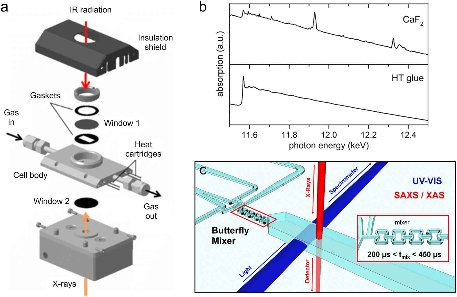 | ||
| Fig. 7 Hybrid devices for XAS and other techniques. (a) Exploded view of a millifluidic gas flow-cell for transmission mode XAS and simultaneous IR spectroscopy (adapted from Chiarello et al. 2014 with the permission of AIP Publishing).173 (b) EXAFS spectra of a Pt/Al2O3 catalyst obtained from the device in (a) with CaF2 windows (top) and CaF2 windows comprising a high temperature (HT) carbon glue bypass for X-ray transmission (bottom). Diffraction from the crystalline CaF2 window produces artefacts in the EXAFS data, which are eliminated by using the HT glue bypass (adapted from Chiarello et al. 2014 with the permission of AIP Publishing).173 (c) Conceptual design of an ultra-fast mixing device for XAS/SAXS/UV-vis analysis of nanoparticle synthesis. The inset shows the design of the butterfly mixing element (adapted with permission from Ramamoorthy et al., 2024; Royal Society of Chemistry).179 | ||
Conversely, Dann et al. designed an aluminum XAS/DRIFTS reactor with a separate CaF2 window for conducting IR analysis and used it to study a Pd–Al2O3 catalyst operating at high temperature.174 A polychromatic X-ray beam passed directly through a thinned section of the Al reactor, where it was used to perform energy dispersive XANES and EXAFS at the Pb K-edge and collect full spectra in only 4.8 ms (for XANES). The gas effluent at the outlet of their device was also directed towards an instrument for performing simultaneous mass spectrometry (MS). Similarly, Venezia et al. developed a silicon-glass millifluidic chip for XAS/DRIFTS/MS analysis that had separate thin silicon windows for the X-ray and IR beams, respectively.175 They also studied the operation of a Pd–Al2O3 catalyst and its performance in two separate reactions. Huyke et al. developed a microfluidic device for performing XAS and XES.176 Their device consisted of a fused silica hydrodynamic flow focusing mixer connected to a Kapton capillary for X-ray analysis. The authors used it to study the reduction of ferricyanide by ascorbic acid with millisecond time resolution.
Several devices have also been designed to support both XAS and SAXS analysis. For example, Karim et al. studied the synthesis of Pd nanoparticles in a silicon-glass microfluidic device with SAXS and fluorescence mode XANES/EXAFS at the Pd K-edge.177 For SAXS analysis, the glass layer was replaced by another Si layer to lower background scattering. Binninger et al. also performed XAS and SAXS with a millifluidic electrochemical flow cell.178 Their device was made from a polyether ether ketone (PEEK) housing that held two electrically conductive Kapton films to serve as both the X-ray windows and electrodes. Using this device, they performed Ir L3-edge (11.22 keV) transmission mode XANES/EXAFS to follow the oxidation state of a mixed Pt/IrO2–TiO2 electrocatalyst as a function of the applied electric potential. In turn, anomalous SAXS was used to follow the degradation of the Pt cathode, where performing SAXS at energies near the Pt L3-edge enabled isolation of the scattering from the Pt nanoparticles from that of the IrO2–TiO2 support. Recently, Ramamoorthy et al. demonstrated an ultra-fast microfluidic mixer for performing XAS, SAXS, and UV-vis analysis with dead times as low as 200 μs (Fig. 7c).179 They used the OSTEMER and Kapton-based device to study the nucleation and growth of Au NPs with transmission mode XANES at the Au L3-edge. With the aid of these three complementary techniques, the authors revealed the formation of transient pre-nucleation clusters and Au(I) lamellar phases prior to the nucleation of Au(0) nanoparticles. Notably, the authors performed both continuous and stopped-flow analysis on-chip to access shorter and longer reaction times, respectively.
4.3 XPCS
X-ray photon correlation spectroscopy (XPCS) has also received some attention in continuous flow micro- and milli-fluidic devices. XPCS is not a true spectroscopy technique based on the measurement of light transmission as a function of wavelength, but rather it is a time spectroscopy.187 Intensity fluctuations, or so-called “speckles”, appearing in X-ray scattering patterns collected over time using coherent X-ray radiation are temporally correlated to extract information on the physical dynamics of a sample, such as related to diffusive or advective motion.182 More simply, the technique is an extension of Dynamic Light Scattering (DLS) into the X-ray regime, where it is useful for analyzing thicker, more turbid samples at smaller spatial scales.188The technique was first performed in flow by Fluerasu and co-workers, who used a simple millifluidic capillary cell to determine the diffusive dynamics of PMMA and latex nanoparticle suspensions.180,181 The authors found that scattering in the direction of the wavevector, q, perpendicular to the flow was insensitive to the advective component of particle motion at low shear rates (“transverse flow geometry”), whereas scattering in the direction parallel to the flow was strongly affected by advection (“longitudinal flow geometry”; Fig. 8). They thus exploited the transverse flow scattering to isolate the thermal motion of the particles and extract diffusion constants. Later, Fluerasu et al. followed up their work by using both the transverse and longitudinal scattering to study the diffusive and advective dynamics of a flow of silica nanoparticles.182 Transverse flow scattering data were used to deconvolute the longitudinal scattering data collected from different radial positions along the cross-section of the flow tube in order to calculate the shear relaxation rate. The rates calculated at each position matched well with a Poiseuille model of the flow.
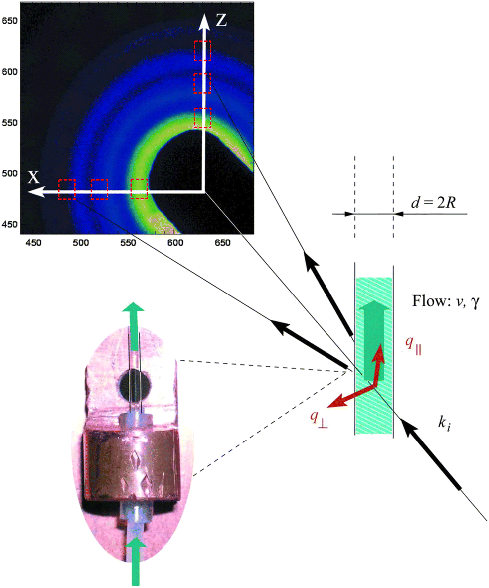 | ||
| Fig. 8 An example of an XPCS flow experiment. Scattering of the incident beam (ki) in the longitudinal (q||) and transverse (q⊥) directions by fluid flowing within the capillary is obtained from averaging of the regions within the dotted lines along the Z and X axes of the area detector, respectively. The photo shows the simple capillary setup of Fluerasu et al. (2008). Adapted with permission of the International Union of Crystallography.181 | ||
More recently, Urbani et al. further miniaturized this technology using a microfluidic chip and a microfocused X-ray beam.183 They mapped the advective dynamics at different channel positions along the chip, including straight and curved sections and a Venturi flow constriction. Flow velocities at the constriction calculated from XPCS data were compared to a CFD model with relatively good agreement, however some deviations were observed, especially at the center of the constriction where velocities were the highest. Lhermitte et al. improved the ability to calculate absolute flow velocities from XPCS data by performing heterodyne analysis, i.e., collecting scattering from the dynamic sample and a static reference material simultaneously.184 This heterodyne XPCS technique was subsequently utilized by Steinrück et al. to measure ion transport within the polymer electrolyte of a lithium-ion battery cell.185 Finally, Muhunthan et al. recently demonstrated a millifluidic flow-cell for performing split-pulse XPCS (sp-XPCS), X-ray pump X-ray probe (XPXP), and SAXS/WAXS measurements under extreme conditions at both synchrotrons and XFELs.186 The cell was constructed from titanium alloy with diamond windows and validated by obtaining speckle patterns from supercritical H2O at 380 °C and 25 MPa.
5 Devices for X-ray imaging
5.1 Brief theory and overview
The field of X-ray imaging comprises a wide variety of techniques that can provide morphological and chemical information on extended samples. These techniques can be divided broadly into two categories: full-field and scanning.189 Full-field techniques make use of an X-ray beam that irradiates an entire sample or region of interest in transmission mode. Conversely, with a scanning technique, a sample is irradiated by a small X-ray beam in a 2D raster pattern, and the image is constructed as a mosaic of the data collected at each position.189,190 Contrast in the image is obtained by recording the absorption or phase shift of X-rays by the sample using a 2D detector. Both of these quantities are related to a material's complex refractive index, n:| n = 1 − δ + iβ | (3) |
With a scanning technique, data can be collected using different geometries and may be composed of single-wavelength absorption contrast measurements, or more commonly, of measurements collected at multiple wavelengths. Scanning instruments making use of other types of detection are also possible and can be used to construct, for example, fluorescence, scattering, or diffraction “maps”. Most techniques can also be made 3D by collecting 2D data (called “projections”) from multiple orientations of a sample under rotation and reconstructing the 3D volume using tomographic algorithms.192
In science and engineering applications, full-field X-ray imaging techniques relying on either phase-shift or absorption contrast are collectively referred to as full-field transmission X-ray microscopy (TXM), while scanning techniques are collectively referred to as scanning transmission X-ray microscopy (STXM). In both cases, the maximum spatial resolution is about 20–50 nm, mainly determined by the imaging zone plate in TXM, and by the focusing zone plate (which dictates the minimum raster step) in STXM. This resolution may be degraded in liquid though, in particular due to Brownian motion.
Owing to the wide variety of specific imaging techniques, this section will be organized by the type and application of the micro/millifluidic device rather than by the specific measurement technique as in the previous two sections. In fact, despite the number of beamlines and devices utilized, most studies have been conducted using similar device styles for similar applications. Specifically, the majority of papers report either thin microfluidic devices for performing TXM and STXM, often for electrochemistry applications, or larger millifluidic flow cells for performing tomographic studies of fluid flow and geochemistry within porous media. More details on all the papers reviewed below can be found in Table 3.
| X-ray technique(s) | Device type | Device material(s) | Fabrication and/or assembly method | Window material, thickness | Geometry, beam pathlength | Sample(s) investigated | Conditions | Beamline, source, X-ray energy | Beam size/resolution | Acquisition mode and exposure time | Ref. |
|---|---|---|---|---|---|---|---|---|---|---|---|
| STXM and XANES | Microfluidic static cell | Silicon | Clamping | Silicon nitride, 2 × 100 nm | Transmission, ∼3 μm | Clay | Ambient temperature & pressure | X1-A, NSLS, C K-edge (283.8 eV) | Unknown | Unknown | Neuhausler et al. (2000)193 |
| TXM | Microfluidic static cell | Polyimide, silicon | Clamping | Si/SixNy-coated polyimide, 2 × 150 nm | Transmission, ∼10 μm | CaCO3 | Ambient temperature & pressure | IRP, BESSY I, “water window” between 282–533 eV | ∼40 nm resolution | Multiframe, 2–10 s per exposure | Rieger et al. (2000)194 |
| Spectro-STXM and XANES | Microfluidic electro-chemical cell | Silicon, poly(chloro-trifluoroethyl-ene) | Epoxy, vacuum grease | Silicon nitride, 2 × 75 nm | Transmission, ∼1 μm | Polyaniline thin film | Ambient temperature & pressure | 5.3.2, ALS, C K-edge (283.8 eV) and N K-edge (401.6 eV) | ∼50 nm resolution | Unknown, <60 s | Guay et al. (2005)195 |
| Spectro-STXM | Millifluidic gas flow cell | Silicon, PDMS, glass | Photolithography, wet etching, plasma etching, sputter coating, micromachining, plasma bonding, adhesive | Silicon nitride, 2 × 100 nm | Transmission, 0.8 mm | Cu catalyst | 260 °C, ambient pressure | 11.0.2, ALS, Cu L3-edge (931.1 eV) | ∼40–100 nm resolution | Multiframe, ∼12 s per image per energy, full spectra in ∼15 min | Drake et al. (2004)196 |
| Spectro-STXM | Microfluidic gas flow cell | Silicon, aluminum, stainless steel, viton | Machining, clamping, glue/wax | Silicon nitride, 2 × 50 nm | Transmission, ∼200 μm | NaBr and diesel soot | 5–27 °C, ambient pressure | PolLux, SLS, O K-edge (532 eV) | 30–40 nm beam spot | Unknown | Huthwelker et al. (2010)197 |
| Ammonium sulfate | Zelenay et al. (2011)198 | ||||||||||
| Spectro-STXM | Microfluidic gas flow cell | Silicon, PEEK or aluminum, viton, PTFE | Machining, clamping, epoxy | Silicon nitride, 2 × unknown | Transmission, ∼0.5–1.5 mm | NaCl | Ambient temperature & pressure | 11.0.2 and 5.3.2.2, ALS, O K-edge (532 eV) | 25 nm outer zone plate width | Multiframe, ∼1 ms per pixel | Kelly et al. (2013)199 |
| Spectro-STXM | Microfluidic gas flow cell | Silicon, glass, brass, viton | Machining, microfabrication, clamping | Silicon nitride, 2 × 10 nm | Transmission, ∼4 μm | Fe-based FTS catalyst | 25–350 °C, ambient pressure | 11.0.2, ALS, C K-edge (283.8 eV), O K-edge (532 eV), and Fe L3- and L2-edges (708.1 and 721.1 eV) | ∼40 nm resolution | Unknown | de Smit et al. (2008)200 |
| Spectro-STXM | Microfluidic gas flow cell | Silicon, glass, brass, viton | Machining, microfabrication, clamping | Silicon nitride, 2 × 10 nm | Transmission, ∼50 μm | Fe-based FTS catalyst | 25–500 °C, ambient pressure | 10ID1, CLS, O K-edge (532 eV), and Fe L3- and L2-edges (708.1 and 721.1 eV) | ∼40 nm resolution | Unknown | de Smit et al. (2009)201 |
| Spectro-STXM | Microfluidic gas/liquid flow cell | Silicon, fluoropolymer O-ring | Photolithography, reactive ion etching, chemical vapor deposition, wet etching, E-beam evaporation, clamping | Silicon nitride, 2 × 50 nm | Transmission, ∼500 nm | CexTiO2-supported Pt catalyst | 140 °C, ambient pressure | 7.0.1.2, ALS, Ti L3- and L2-edges (455.5 and 461.5 eV), Ce M5-edge (883.8 eV), and Pt L3-edge (11.56 keV) | ∼55 nm resolution | Multiframe, 0.1–2 ms per pixel | Yoo et al. (2020)202 |
| TXM | Microfluidic continuous flow cell | Silicon, stainless steel, unknown O-ring material | Machining, clamping, glue | Silicon nitride, 2 × 100 nm | Transmission, unknown | Ag nanowires reacting with Au | Ambient temperature & pressure | Unknown beamline, APS, 12 keV | ∼25 nm resolution | Multiframe, 0.5 Hz | Sun and Wang (2011)203 |
| Spectro-STXM and μXAS | Microfluidic electro-chemical cell | Silicon, SU-8, NOA 84 | Photolithography, UV curing | Silicon nitride, 2 × Unknown | Transmission, unknown | Co-polypyrrole electrocatalyst | Ambient temperature & pressure | TwinMic, Elettra, Co L3-edge (778.6 eV) | Unknown | Unknown | Bozzini et al. (2014)236 |
| Spectro-STXM | Microfluidic electro-chemical cell | Silicon, fluoropolymer O-ring | Photolithography, reactive ion etching, chemical vapor deposition, wet etching, E-beam evaporation, clamping | Silicon nitride, 2 × 75 nm | Transmission, ∼1 μm | LiXFePO4 crystals | Ambient temperature & pressure | 11.0.2.2 and 5.3.2.1, ALS, Fe L3-edge (708.1 eV) | 50 nm beam spot | Multiframe, 1 ms per pixel | Lim et al. (2016)204 |
| Spectro-STXM | Microfluidic electro-chemical cell | Silicon, fluoropolymer O-ring | Photolithography, reactive ion etching, chemical vapor deposition, wet etching, E-beam evaporation, clamping | Silicon nitride, 2 × 100 nm | Transmission, ∼1 μm | Co(OH2) crystals | Ambient temperature & pressure | 11.0.2, ALS, Co L3-edge (778.6 eV) | 50 nm resolution | Multiframe, 2 ms per pixel + 2 ms delay, full spectra in ∼30 min | Mefford et al. (2019)205 |
| Mefford et al. (2021)206 | |||||||||||
| Spectro-STXM | Microfluidic electro-chemical cell and microfluidic gas flow cell | Silicon, viton, unknown housing material | Machining, clamping, tape | Silicon nitride, 2 × 100 nm | Transmission, ∼20 μm | FeSO4 solution, polymer | Ambient temperature & pressure | BL4U, UVSOR-III, C K-edge (283.8) and Fe L3-edge (708.1 eV) | ∼40–50 nm resolution | Unknown | Ohigashi et al. (2016)207 |
| Spectro-STXM | Microfluidic electro-chemical cell | Silicon, acrylic polymer resin, unknown O-ring material | 3D printing, proprietary techniques, clamping | Silicon nitride, 2 × 50 nm | Transmission, ∼1–1.5 μm | Cu deposition on Au electrode | Ambient temperature & pressure | 10ID1, CLS, Cu L3-edge (931.1 eV) | ∼25 nm resolution | Multiframe, ∼20 s per image | Prabu et al. (2018)208 |
| Spectro-STXM | Microfluidic continuous flow reactor | Silicon, PDMS, PTFE, stainless steel | Machining, soft lithography, clamping | Silicon nitride, 2 × 50 nm | Transmission, 3 μm | CaCO3 with polymer additive | Ambient temperature, ≤1 bar pressure drop | PolLux, SLS, Ca L3- and L2-edges (346.4 and 350 eV) | ∼43 nm resolution | Multiframe, ∼5–50 ms per pixel, ∼5–11 min per image | Gosse et al. (2020)89 |
| HERMES, SOLEIL, 510 eV and Ca L3- and L2-edges (346.4 and 350 eV) | ∼37–60 nm resolution | ||||||||||
| X-ray PIV (2D) | Millifluidic continuous flow | PTFE tubing | Unknown | PTFE, unknown | Transmission, 750 μm | Alumina microspheres | Ambient temperature & pressure | 1B2, Pohang Light Source, “white beam” | 12.3 μm resolution | Multiframe, 50 Hz | Lee and Kim (2003)209 |
| X-ray PIV (3D) | Microfluidic continuous flow | Silicone tubing | Unknown | Silicone, unknown | Transmission, 490 μm | Aluminum or solder microparticles | Ambient temperature & pressure | XOR-32-ID, APS, 18 keV | 3.87 μm pixel size | Multiframe, 60 Hz | Lee et al. (2011)210 |
| μCT | Millifluidic flow cell | Polyethylene, unknown | Unknown | Polyethylene, unknown | Transmission, 6.5 mm | Multiphase flow in porous polyethylene | Ambient temperature & pressure | X2B, NSLS, unknown | 4.1 μm voxel size | Multiframe, collection of tomograms after each injection | Prodanović et al. (2006)211 |
| μCT | Millifluidic flow cell | Silicone, PTFE, epoxy resin | Epoxy, compression fittings | Silicone and PTFE, unknown | Transmission, 9 mm | Carbonated salt solution in limestone core | Ambient temperature, 0–3 MPa pressure | ID19, ESRF, 40 keV | 6 μm resolution | Multiframe, collection of tomograms at six time points | Noiriel et al. (2007)212 |
| Fast-μCT | Millifluidic flow cell with integrated pumps | Polycarbonate, unknown | Unknown | Polycarbonate, unknown | Transmission, 4 mm | Multiphase flow in sandstone | Ambient temperature, <10 kPa | TOMCAT, SLS, 21.25 keV | 3 μm voxel size | Multiframe, 12 ms per projection, 16.8 s tomogram acquisition | Berg et al. (2013)213 |
| Fast-μCT | Millifluidic flow cell with integrated pumps | Unknown | Unknown | Unknown | Transmission, 4 mm | Multiphase flow in Robuglas | Ambient temperature, <10 kPa | TOMCAT, SLS, 36 keV | 2.11 μm pixel size | Multiframe, 40 ms per projection, continuous collection over 12 min | Armstrong et al. (2014)214 |
| Fast-μCT | Millifluidic flow cell | PEEK | Compression fittings | PEEK, unknown | Transmission, 4.8 mm | Multiphase flow in glass bead column | Ambient temperature, 517.1 kPa pressure | I22, diamond, unknown | 3.25 μm resolution | Multiframe, 6 s tomogram acquisition | Hasan et al. (2020)215 |
| Fast-μCT | Millifluidic passive wicking cell | PMMA with organic binders | Powder-based 3D printing | No window | Transmission, 2 or 3.5 mm depending on the orientation | Water in porous microbead column | Ambient temperature & pressure | ID19, ESRF, 40 keV “pink beam” | 1.1 μm pixel size | Multiframe, 0.5 s tomogram acquisition with 12 s read-out time | Piovesan et al. (2020)216 |
| Fast-μCT | Millifluidic gravity-feed flow cell | PMMA | Compression fittings | PMMA, unknown | Transmission, 6 and 25 mm | Multiphase flow in sandstone gravel column | Ambient temperature & pressure | I12, diamond, “white beam” between 50 and 150 keV or monochromatic beam of unknown energy between 53 and 150 keV | 2.5 to 3.8 μm voxel size | Multiframe, 90–200 μs per projection, 0.05 to 0.5 s tomogram acquisition | Dobson et al. (2016)217 |
| Tomographic X-ray PIV | Millifluidic high-pressure flow cell (Hassler core holder) | Viton, PEEK | Compression fittings | Viton, PEEK, unknown | Transmission, 4 mm | Multiphase flow containing silver-coated hollow glass tracer particles in sintered glass filter and limestone | Ambient temperature, 2 MPa pressure | TOMCAT, SLS, glassy carbon and borosilicate filtered “white beam” | 2.75 μm voxel size | Multiframe, 0.5 ms per projection, 0.25–0.5 s tomogram acquisition | Bultreys et al. (2024)218 |
| μCT | Microfluidic continuous flow mixer (Kenics mixer) | IP-S resin | Two-photon stereolithography, UV curing, epoxy | IP-S resin, unknown | Transmission, 200 μm | Mixing of two aqueous phases | Ambient temperature & pressure | P05, PETRA III, 11 keV | P05: 1.14 μm voxel size | P05: multiframe, 2 s per projection, ∼2.5 tomogram acquisition | Knoška et al. (2020)219 |
| TOMCAT, SLS, 18 keV | TOMCAT: unknown | TOMCAT: 80 ms per projection | |||||||||
| μCT | Millifluidic high pressure flow cell | Epoxy resin, other unknown materials | Compression fittings | Epoxy resin, unknown | Transmission, 9 mm | Carbonated salt solution in limestone core | Ambient temperature, 0.13 MPa back pressure | ID19, ESRF, 40 keV | 6 μm resolution | Multiframe, collection of tomograms at six time points | Noiriel et al. (2013)220 |
| μCT | Millifluidic flow cell | Quartz tube | Sintering, compression fittings | Quartz, 1.4 mm wall | Transmission, 1.6 mm | BaSO4 in microporous quartz column | Ambient temperature & pressure | 13-ID-B, APS, 22 keV | 1.24 μm voxel size | Multiframe, collection of tomograms every 24 min | Godinho et al. (2016)221 |
| Fast-μCT | Millifluidic high-pressure flow cell (Hassler core holder) | Stainless steel, aluminum, steel wire, silicone, heat-shrink tubing and O-rings of unknown material | Machining, compression fittings | Aluminum, silicone, shrink wrap, unknown | Transmission, 3 mm | Salt solution in olivine rock | 200 °C, 10 MPa fluid pressure and 15 MPa confining pressure | 2-BM, APS, 65 keV “pink beam” | 1.47 μm pixel size | Multiframe, 10 ms exposure per projection, 20 s tomogram acquisition | Fusseis et al. (2014)222 |
| X-ray lamino-graphy | Microfluidic packed-bed reactor | Silicon, glass (Pyrex) | Photolithography, wet etching, anodic bonding | Glass, unknown, silicon, unknown | Transmission, 30 μm | CaCO3 | Ambient temperature & pressure | ID19, ESRF, 26 keV | 0.7 μm resolution | Unknown | Morais et al. (2023)223 |
| μCT | Millifluidic passive counter-diffusion cell | Tygon tubing, heat-shrink tubing | Heat-shrinking | Heat-shrink tubing, unknown | Transmission, 3 mm | BaSO4 in shale | Ambient temperature & pressure | I13-2, diamond, 27.6 keV “pink beam” | 1.6 μm voxel size | Multiframe, 100 ms exposure per projection, 80 s tomogram acquisition | Godinho et al. (2019)224 |
| μCT and XRD-CT | Millifluidic passive counter-diffusion cell | Glass tubes, His-3 BAG heat-shrink tubing, silicone tubing | Heat-shrinking | No window | Transmission, 2.8 mm | CaSO4·xH2O in CPG rod | Ambient temperature & pressure | μCT: I13-2, diamond, unknown | μCT: 1.6 μm pixel size | μCT: multiframe, 100 ms exposure per projection, 80 s tomogram acquisition | Anduix-Canto et al. (2021)225 |
| XRD-CT: ID11, ESRF, 40 keV | XRD-CT: 50 μm × 50 μm beam size | XRD-CT: single-shot, 1 s exposure per grid point | |||||||||
| Scanning μXRF and XAS | Microfluidic continuous flow mixer | PDMS, silicon, O-rings and holder of unknown materials | Soft lithography, machining, clamping, compression fittings | Silicon nitride, 100 nm | Fluorescence, 87.2 μm | Water and pyridine | Ambient temperature & pressure | BL3U, UVSOR-III, N K-edge (401.6 eV) and O K-edge (532 eV) | 30 μm × 30 μm, beam size, 30–61 μm step size | Unknown | Nagasaka et al. (2019)226 |
| Scanning μXRF, SAXS/WAXS, and XRD | Microfluidic continuous flow mixer (and others) | PDMS, Kapton, 3D-printed resin, O-ring of unknown materials | Soft lithography, plasma bonding, 3D printing, clamping, gluing, compression fittings | Kapton, 8 μm, PDMS, 30 μm | Fluorescence, >500 μm | Iron oxide NPs | Ambient temperature & pressure | LUCIA, Soleil, Fe K-edge (7.11 keV) | 3.5 μm × 3.5 μm beam size, 5 μm step size | Single-shot, 300 ms exposure per grid point | Chaussavoine et al. (2020)227 |
| Scanning μXRF and XAS | Microfluidic continuous flow cell | Silicon, AF-32 Eco glass | Photolithography, reactive ion etching, machining, plasma ashing, muffle urnace firing, epoxy, UV epoxy, compression fittings | Glass, 30 μm | Fluorescence, >30 μm | Fe–As–S geochemical reactions | Ambient temperature & pressure | 4-BM, NSLS-II, 14 keV (for μXRF mapping) | 5 μm × 5 μm beam size, 5–45 μm step size | Single-shot, 50–200 ms exposure per grid point | Chen and Kocar (2021)228 |
| Scanning nano-XRF | Microfluidic electro-chemical cell | Glass, NOA, PET, PDMS | Photolithography, wet etching, sputter coating, machining, UV epoxy | Glass, ≤1 μm, PET, 12 μm | Fluorescence, ∼20–50 μm | Electrodeposition of Ag/AgCl | Ambient temperature & pressure | Carnaúba, Sirius, 9.7–13.7 keV | 600 nm × 600 nm beam size, 5 μm step size | Single-shot, 22.5 ms per grid point, 62 s for full map | Neckel et al. (2021)229 |
| XFEL-CDI | Microfluidic continuous flow cell | Silicon, Kapton | Unknown | Silicon nitride, 2 × 200 nm | Transmission, 12 μm | Ag NPs | Ambient temperature, ambient to vacuum pressure | BL2, SACLA, 4 keV | 100 nm × 100 nm beam size | Single-shot, 10 fs | Matsumoto et al. (2022)230 |
5.2 Devices for STXM and TXM
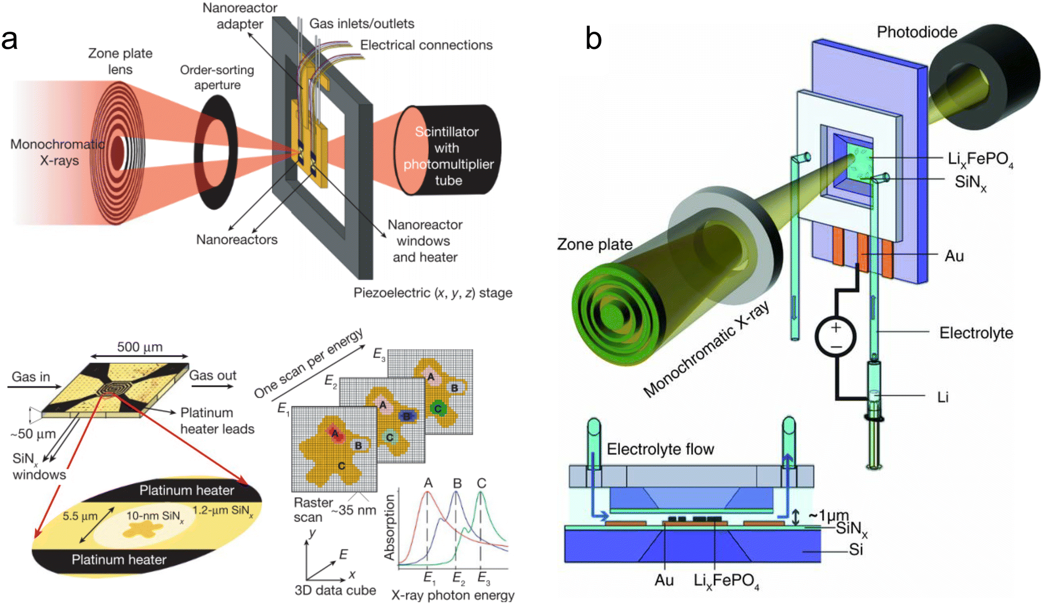 | ||
| Fig. 9 Microfluidic devices for operando TXM/STXM. (a) A STXM setup with a MEMS gas nanoreactor for studying catalysis at high temperature (top). The inset shows a detailed illustration of the Pt electrode design and the SixNy windows (bottom left) and an example of spectro-STXM data from a heterogeneous catalyst particle (bottom right) (reprinted with permission from de Smit et al. 2008; Copyright 2008 Springer Nature).200 (b) An electrochemical STXM setup based on a Si/SixNy chip for studying Li-ion battery particles. The inset shows the side view of the device and the ∼1 μm spacing between the SixNy windows (from Lim et al., 2016; reprinted with permission from AAAS).204 | ||
De Smit et al. adapted a micro-electromechanical systems (MEMS) cell designed for transmission electron microscopy (TEM)235 to perform the first spectro-STXM study of a working catalyst (Fig. 9a).200 They studied an iron-based catalyst during a Fischer–Tropsch synthesis (FTS), which is used to convert CO and H2 gas into hydrocarbon products. Imaging the catalyst at the C K-edge, O K-edge and Fe L2- and L3-edges enabled them to quantify the different iron phases formed and investigate their contribution to the FTS reaction. The same team followed up this work by imaging a single catalyst particle at different FTS reaction temperatures up to 500 °C.201 Yoo et al. also adapted a commercial cell designed for TEM to study the oxidation of CO gas by a TiO2-supported Pt catalyst.202 By using STXM at the Ce M-edge, they showed that doping of the TiO2 support with Ce encouraged the formation of highly efficient Pt single atoms at CeOx–TiO2 interfaces.
Lim et al. used a commercial electrochemical flow-cell to study single Li-ion battery particles under charging and discharging cycles (Fig. 9b).204 STXM enabled them to observe spatial heterogeneities in Li composition arising from non-uniform rates of lithiation and delithiation, which could affect battery performance and safety. Similarly, Mefford et al. used the same electrochemical flow cell to study compositional heterogeneities and the resulting catalytic heterogeneities within electrocatalyst single crystals.205,206 Other microfluidic electrochemical cells for TXM/STXM have been reported for studying electrode–electrolyte interactions,207 including the hybrid device of Prabu et al., which combined a Si/SixNy type chip with a 3D-printed holder for making world-to-chip connections.208
In contrast to most of the flow devices we have reviewed for scattering and spectroscopy, which were designed for rapid fluid mixing, most in situ TXM/STXM—and even TEM—studies have not been focused on flow management. This is likely because the reactions of interest were initiated by localized heating or an applied voltage rather than by the mixing of chemical reactants, and simply ensuring the replenishment of an electrolyte was sufficient for device operation. In this context, Gosse et al. presented a Si/SixNy type device for STXM designed to study precipitation reactions with precise flow control.89 By using a pressure-actuated, rather than syringe-driven, system with flow meters upstream and downstream of the chip, the authors demonstrated the ability to adjust or stop flows within seconds. They also showed that the liquid within the Si/SixNy cell could be completely refreshed in less than two minutes using flows of only a few microliters per minute.
5.3 Tomography for flow imaging
Around the same time, work was beginning in the geological community to visualize processes within porous rocks that were also inaccessible to light microscopy. X-ray micro-computed tomography (μCT) was already an established method for investigating the internal 3D microstructure of geological samples. The next step was to combine it with a fluidic sample environment to perform dynamic studies. Cylindrical rock cores with diameters on the millimeter scale are thin enough to allow the transmission of hard X-rays, and they can also be assembled into simple millifluidic devices by sealing the sides with an epoxy resin and making fluid connections at both ends. Early work in this area required the sample to be alternatively applied with a flow and then taken to the beamline for imaging due to the difficulty of attaching flow equipment to a rotating tomography stage.239 Subsequent studies, such as from Prodanović et al.211 and Noiriel et al.,212 were performed in situ but not operando, in that the devices were mounted on the stage during flow, but the flows were stopped during imaging. Thus, the difficultly of connecting the flow apparatus to the sample stage and the long acquisition times required to obtain a full tomogram continued to limit the potential time-resolution of the technique.
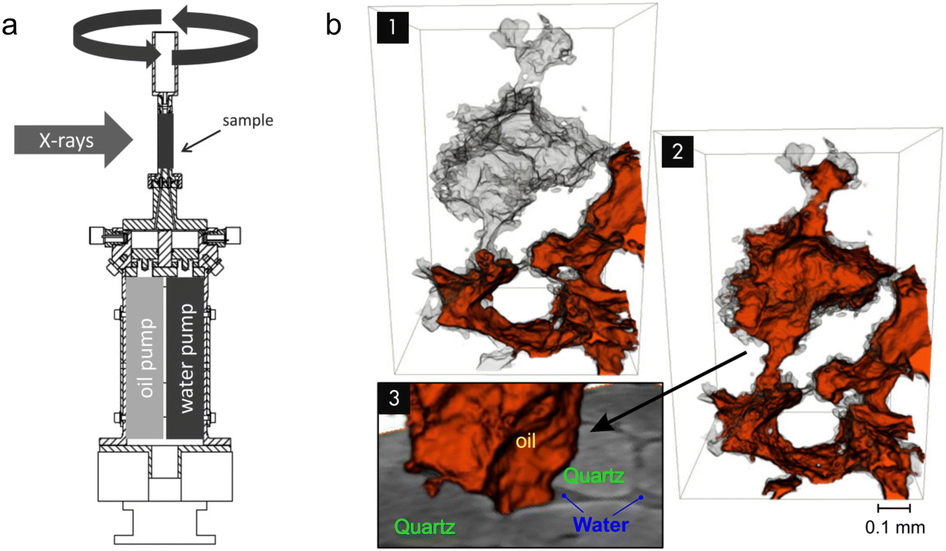 | ||
| Fig. 10 Operando X-ray micro-computed tomography. (a) An integrated millifluidic device for fast-μCT that can be mounted on a rotated tomography stage without external connections (adapted with permission from Armstrong et al. 2014; Copyright 2014 John Wiley and Sons).214 (b) Drainage of water (gray) and infilling of oil (red) within sandstone pores observed with fast-μCT (1–2). (3) Cross-section at a pore throat showing the three phases (water, oil, and quartz rock) (used with permission from Berg et al. 2013; Copyright 2013 The Authors).213 | ||
The time resolution of full tomograms has continued to increase. For example, Hasan et al. used fast-μCT to study solute transport in water-saturated and -unsaturated porous media with a full-tomogram time resolution as short as 6 s.215 Piovesan et al. fabricated a porous millifluidic device using a powder-based 3D printer and used it to study capillary wicking in 3D.216 They performed fast-μCT with sub-second time resolution, however, the readout time of the detector limited the frequency of tomogram acquisition, requiring a 12 s time step between consecutive tomograms. To the best of our knowledge, Dobson et al. performed the first operando fast-μCT experiment with both a sub-second time resolution and time step, with full-tomogram acquisition frequencies up to 20 Hz.217 More recently, Bultreys et al. combined earlier work in 2D X-ray PIV with fast-μCT to perform the first synchrotron-based 3D X-ray PIV study of flow within porous media.218 They imaged multiphase flows containing tracer particles within limestone and sintered glasses and obtained tomograms with 0.25 s time resolution at an acquisition rate of 4 Hz. Many additional studies of hydrology in porous media have been conducted using fast-μCT and millifluidics and cannot all be covered here.242–247 To our knowledge, the only microfluidic μCT study of fluid transport was reported by Knoška et al., who characterized the flow within a helical Kenics mixer by merging streams of low-contrast water and a high-contrast KI solution.219 Due to the steady-state concentration profile of the flows in the static mixer, standard μCT with an acquisition time of ∼2.5 h was sufficient to capture the mixing process.
To investigate diffusive- rather than advective-driven transport processes in samples with smaller pore sizes, several researchers fabricated simple counter-diffusion-based devices. These devices are easier to set up at tomography beamlines than their flow-based counterparts since it is not necessary to mount pumps on the sample stage or connect devices to external equipment. For example, Godinho et al. made a passive-diffusion cell by connecting short sections of tubing to both sides of a 3 mm-diameter shale sample containing micrometer-scale fractures and sub-micron sized pores.224 The tubing sections served as fluid reservoirs containing counter-ions, which were allowed to diffuse into the sample, and the whole assembly was mounted vertically on the stage using one of the tubes as the support. Using this device, the authors continued their μCT studies of BaSO4. They observed that as Ba2+ and SO42− ions diffused and reacted within the sample, barite precipitated first within the larger fractures and then later in smaller fractures and pores.
Anduix-Canto et al. used a similar setup to study the precipitation of calcium sulfate within controlled porous glass (CPG) rods with an average pore diameter of 7 nm.225 The authors performed not only μCT, but also X-ray diffraction computed tomography (XRD-CT) to reveal both the morphology and crystal structure of the phases that precipitated over time. Utilization of CPGs enabled the authors to confine the solution within nanopores that were completely isolated from macropores, and this nanoscale confinement effect led to the precipitation and stabilization of normally unstable amorphous and hemihydrate CaSO4·xH2O phases. The field of geological μCT is a large area, often on the border between milli- and “macro”-fluidics, and thus cannot be completely covered here. The reader is directed to other reviews for further information.246,249
5.4 Other scanning techniques
In addition to absorption- and phase-contrast X-ray imaging and tomography, several microfluidic studies have made use of the spatially resolved acquisition of other types of X-ray data. The most popular approach in the physical sciences has been using scanning μXRF to map micromixers and visualize the concentration profiles of chemical species. Such an approach was implemented by Nagasaka et al., who utilized a microfluidic device comprising a PDMS microchannel and a silicon nitride window to study the mixing of pyridine and water.226 They first mapped the steady-state laminar microflow by μXRF and then obtained N K-edge XAS spectra at different points across the width of the microchannel to determine the local pyridine concentration. Similarly, Chaussavoine et al. developed a vacuum-compatible microfluidic device for studying the synthesis of iron (hydr)oxide nanoparticles.227 They performed μXRF of the channel and identified regions of interest at which to acquire full Fe K-edge XANES spectra using fluorescence read-out. This approach was also utilized in several studies previously reviewed in section 4.156,171,172Scanning μXRF has also been used to study spatial heterogeneities within planar microfluidic devices. For example, Chen and Kocar investigated Fe–As–S geochemical reactions using devices containing arrays of quartz micro-posts as models of porous rock.228 First, the authors would mix a basal salts solution (BSS) with an Fe2+ solution to precipitate iron (hydr)oxides. Subsequently, As- and S-containing solutions were introduced along with NaBr as a flow tracer, and the resulting flow profiles and sorption of As/S were visualized by μXRF (Fig. 11). Similarly, Neckel et al. used scanning XRF to map the electrodeposition of Ag/AgCl films within a microfluidic electrochemical cell.229 They utilized a nanobeam to obtain maps of Ag nucleation sites with sub-micron resolution.
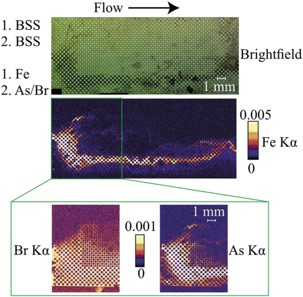 | ||
| Fig. 11 Scanning μXRF within a microfluidic device containing micro-post arrays. Brightfield optical image illustrating the flow direction and chemical addition (top). Model geochemical reactions in the Fe–As–S system are monitored using the appropriate Kα fluorescence peak (bottom and insets). Br is utilized as a flow tracer (reproduced with permission from Chen and Kocar, 2021; International Union of Crystallography).228 | ||
Finally, in an interesting recent study, Matsumoto et al. utilized a multi-window Si/SiyNx microfluidic device at an XFEL to perform coherent diffraction imaging (CDI) of nanoparticle aggregation.229 Two separate suspensions of spherical and rod-shaped gold nanoparticles, respectively, were stored on-chip. Mixing of the solutions was initiated by an XFEL pulse breaking a silicon nitride window at the end of the flow channel and rapidly depressurizing the device under vacuum. Once a flow was established, the device was scanned upstream along the channel to image particles under different aggregation states. To our knowledge, this may be the only example of on-chip microfluidic analysis at an XFEL, and it illustrates a creative way to overcome the challenge of X-ray pulse-induced device damage through experimental design.
6 Developments in laboratory-based analysis
In this final review section, we will look at developments in performing in situ micro- and milli-fluidics experiments in the ‘home’ laboratory, that is, using laboratory X-ray instruments rather than large-scale facilities. Even researchers and institutions with strong official links to a synchrotron radiation facility cannot expect more than a few weeks of beamtime per year under normal circumstances. For other researchers and relative newcomers to user facilities, more than a few days per year might be a luxury. Conducting an experiment with a complex sample environment at another institution also requires a great deal of planning, set-up, and hard work. Additionally, one may utilize unfamiliar equipment or software and rely heavily on the help of local staff, who will have varying levels of investment in user experiments. These are just a few of the many reasons why researchers are interested in the ability to perform microfluidics experiments—and in situ experiments in general250,251—in a laboratory setting.Fortunately, there have been substantial improvements in laboratory X-ray sources and hardware over the past decade and a half. First and foremost, the flux of rotating anode and liquid metal jet X-ray sources has approached that of second-generation synchrotron facilities,11 achieving up to ∼109 photons per second at the sample depending on the source type and collimation/focusing optics.15,252 State-of-the-art sealed tube sources are also improving and able to reach the ∼107–108 range. Multilayer optics and scatterless slits have provided better quality beams,253,254 and sensitive, low-noise, hybrid photon counting detectors used at synchrotrons are now commonly employed on laboratory systems.255,256 Further, current commercial systems offer better software and increased functionality, automation, and sample control, reducing the need to build custom platforms. All these factors have increased the performance and user-friendliness of laboratory X-ray instruments, resulting in renewed interest in using them to perform operando experiments. While they still cannot compete with third- and fourth-generation synchrotrons in terms of flux or coherence, more and more micro- and milli-fluidics experiments are becoming feasible in the laboratory, as the papers reviewed below demonstrate (Table 4). Here, we will again cover progress in scattering/diffraction, spectroscopy, and imaging, and we will also include biological and soft matter applications since, to our knowledge, laboratory X-ray analysis in these areas has not been reviewed previously. Where possible we will also compare the data quality and time resolution of laboratory-based studies to similar synchrotron experiments.
| X-ray technique(s) | Device type | Device material(s) | Fabrication and/or assembly method | Window material, thickness | Geometry/mode, beam pathlength | Sample(s) investigated | Conditions | Instrument, source, detector | Beam size/resolution | Acquisition mode, exposure time | Ref. |
|---|---|---|---|---|---|---|---|---|---|---|---|
| SAXS | Millifluidic continuous flow reactor | Teflon tubing, quartz capillary, commercial micromixer | Components connected by tubing, compression fittings | Quartz capillary, 10 μm wall | Transmission, 1–3.8 mm | Au NPs and Ag NPs | Ambient temperature & pressure | SAXSess (Anton Paar), sealed tube source (PANalytical, 8.04 keV), CCD detector (Roper Scientific) | Unknown | Multiframe, 20 × 10 s | Polte et al. (2010)257 |
| Polte et al. (2012)258 | |||||||||||
| SAXS | Millifluidic continuous flow reactor | Teflon tubing, quartz capillary, commercial micromixer | Components connected by tubing, compression fittings | Quartz capillary, 10 μm wall | Transmission, 1 mm | Pd NPs | Ambient temperature & pressure | SAXSess (Anton Paar), sealed tube source (PANalytical, 8.04 keV), CCD detector (Roper Scientific) | Unknown | Multiframe, unknown | Kettemann et al. (2015)259 |
| SAXS/WAXS | Millifluidic continuous flow reactor | Teflon, polyethylene tubing, quartz capillary | Components connected by tubing, compression fittings | Quartz capillary, 10 μm wall | Transmission, 1 mm | Au NPs | 22, 33, and 45 °C, pressure | Double Ganesha AIR (SAXSLAB), rotating anode source (Rigaku, 8.04 keV), hybrid-photon counting detector (Dectris) | Unknown | SAXS: multiframe, 60, 300, or 600 s exposures depending on the condition and reaction time | Chen et al. (2015)260 |
| WAXS: unknown | |||||||||||
| SAXS/WAXS | Millifluidic continuous flow reactor | Teflon, polyethylene tubing, quartz capillary | Components connected by tubing, compression fittings | Quartz capillary, 10 μm wall | Transmission, 1 mm | ZnO NPs | 40 and 50 °C, pressure | Double Ganesha AIR (SAXSLAB), rotating anode source (Rigaku, 8.04 keV), hybrid-photon counting detector (Dectris) | Unknown | SAXS: multiframe, 30, 60, or 600 s exposures depending on the reaction time | Herbst et al. (2019)261 |
| WAXS: multiframe, 1200 s exposures | |||||||||||
| SAXS | Millifluidic electrochemical flow cell | PEEK, Kapton (gold-coated) | Machined, clamped | Kapton, 2 × 50 μm | Transmission, 50–123 μm of catalyst, 2 mm of electrolyte | Pt NPs on a carbon support | Ambient temperature & pressure | X'Pert Pro (PANalytical), sealed tube source (PANalytical, 8.04 keV), 1D solid-state detector (PIXcel) | Unknown | Multiframe 7 × 1 h | Tillier et al. (2016)262 |
| SAXS | Millifluidic high performance liquid chromoto-graphy system | Unknown | Compression fittings connecting multiple commercial devices | Glass capillary, unknown wall | Transmission, unknown | Proteins | Ambient temperature & pressure | BioXolver L (Xenocs), liquid metal jet source (Excillum, 9.25 keV) | ∼1 mm × 1 mm | Single-shot, 60 s | Bucciarelli et al. (2018)263 |
| SAXS | Millifluidic continuous flow mixer | PMMA, quartz capillary | Unknown | Quartz capillary, unknown wall | Transmission, 2 mm | SiO2 NPs and human serum albumin | Ambient temperature & pressure | NanoStar (Bruker), microfocus source (8.04 keV), 2D gas-based detector (VÅNTEC-2000) | ∼300 μm diameter | Single-shot, 2.5–30 h | Anaraki et al. (2020)264 |
| SAXS | Millifluidic continuous flow reactor | Glass capillary, PTFE tubing, polymer fittings | Compression fittings, tubing coiling | Quartz capillary, 10 μm wall | Transmission, 1 mm | Iron oxide NPs | 60 °C, ambient pressure | SAXSess (Anton Paar), sealed tube source (GE, 8.04 keV), 1D solid-state detector (Dectris) | 17 mm × 0.25 mm | Single-shot, 60 s | Besenhard et al. (2020)127 |
| SAXS | Microfluidic segmented flow | OSTEMER 322 | Photolithography, soft lithography, cured and laminated | OSTEMER 322, 2 × 200 μm | Transmission, 150 μm | Device materials | Ambient temperature & pressure | Xeuss 2.0 (Xenocs), sealed tube source (Xenocs, 8.04 keV), hybrid photon counting detector (Dectris) | Unknown | Multiframe, 500 s total scan time | Lange et al. (2020)92 |
| Micro-XRD | Microfluidic electro-chemical cell | PVC, brass, graphite | Machining, clamping, pressure fittings, conductive epoxy | Kapton, unknown, graphite, 500 μm | Transmission, ∼400 μm | Iron and iron oxide phases | Ambient temperature & pressure | Custom diffractometer, rotating anode source (Rigaku, 17.4 keV), image plate detector (unknown) | 400 μm diameter or 20 × 20 μm | Multiframe, 20 min scan time | Monnier et al. (2008)163 |
| Monnier et al. (2014)164 | |||||||||||
| SAXS | Microfluidic evaporative flow | PDMS | Photolithography, soft lithography, plasma bonding | PDMS, ∼150 μm | Transmission, 25 μm | Au colloidal supercrystals | Ambient temperature & pressure | Rotating anode source (Rigaku, 8.04 keV), hybrid-photon counting detector (Dectris) | ∼0.5 mm × 0.5 mm | Single-shot, ∼3.5 min | García-Lojo et al. (2021)265 |
| SAXS | Millifluidic flow dialysis device | COC, commercial dialysis insert | 3D printing | COC, 2 × 50 μm | Transmission, 12 mm | Lipids and polymers | Ambient temperature & pressure | Microfocus source (Xenocs, 17.4 keV), unknown detector | Unknown | Multiframe, 360 × 1 min | Ehm et al. (2022)266 |
| Single-shot, 20 min | |||||||||||
| SAXS/WAXS and PXRD | Microfluidic segmented flow | PMMA, PTFE, Kapton, silicone | UV laser cutting, clamped, compression fittings | Kapton, 2 × 75 μm | Transmission, 300 μm | CaCO3 with nucleating agents, silica NPs | Ambient temperature & pressure | Xeuss 2.0 (Xenocs), liquid metal jet source (Excillum, 9.25 keV), hybrid photon counting detector (Dectris) | ∼250 μm × 250 μm | Multiframe, 60 × 0.5 s | Levenstein et al. (2022)15 |
| Milli-fluidic segmented flow | Kapton capillary | Interference fit, compression fittings | Kapton capillary, 100 μm wall | Transmission, 1 mm | Calcite and paracetamol crystals | XtaLab Synergy R or Synergy Custom (Rigaku), microfocus rotating anode source (Rigaku, 8.04 keV), hybrid photon counting detector (Rigaku) | ∼140 μm × 140 μm | Multiframe, 3600 × 25 ms | |||
| SAXS | Microfluidic continuous flow | OSTEMER, Kapton | Photolithography, PDMS injection molding, cured, cure-bonded | OSTEMER, 2 × 50 μm and Kapton, 25 μm | Transmission, 400 μm | Au NPs, silica NPs, BSA protein, latex NPs | Ambient temperature & pressure | Xeuss 2.0 (Xenocs), microfocus source (Xenocs, 8.04 keV), hybrid photon counting detector (Dectris) | 250 μm × 250 μm | Single-shot, 10–60 min | Radajewski et al. (2023)267 |
| SAXS | Millifluidic continuous flow reactor | PFA tubing, glass capillary | Compression fittings, tubing coiling | Glass capillary, unknown wall | Transmission, unknown | Polymer nano-objects | 75 °C, 6.9 bar backpressure | Xeuss 3.0 (Xenocs), liquid metal jet source (Excillum, 9.25 keV), hybrid photo counting detector (Dectris) | 0.4 mm diameter | Single-shot, 5 min | Guild et al. (2023)268 |
| PXRD | Various micro- and milli-fluidic devices | Various | Various | Various | Various | Calcite, theophylline, KNO3, Na2SO4 | Various | XtaLab Synergy Custom (Rigaku), microfocus rotating anode source (Rigaku, 8.04 keV), hybrid photon counting detector (Rigaku) | 150 μm diameter, tunable | Multiframe, 18 s exposure per frame | Turner et al. (2024)269 |
| XANES | Millifluidic photocatalysis cell | Unknown body material, scotch tape | 3D printing (DLP), clamping, tape | Scotch tape, unknown | Fluorescence, unknown | Pt catalyst on TiO2 support | Ambient temperature, Ar atmosphere | R-XAS Looper (Rigaku), unknown source at Pt L3-edge, silicon drift detector | Unknown | Single-shot, ∼1–2 min | Kozyr et al. (2023)270 |
| XRF | Capillary electro-phoresis cell | Fused silica capillary with polyimide coating | Capillary mounted in plastic housing | Fused silica capillary with polyimide coating, 33.5 μm wall thickness | Fluorescence, unknown | Free and complexed metal ions | Ambient temperature & pressure | Eagle II (EDAX), Rh target excitation source (EDAX), SiLi detector (EDAX) | ∼50 μm spot | Multiframe, 10 s dwell time for full spectra | Miller et al. (2003)271 |
| μXRF and XRD | Miniaturized XRF chip | Glass, PDMS, lead | Various | Glass, unknown | Fluorescence, unknown | Metal foils | Ambient temperature & pressure | XRD spectrometer with HPGe detector (Canberra Industries) | Uncollimated radiation from Am source | Unknown | Greaves and Manz (2005)18 |
| Various millifluidic XRD chips | Polycarbonate, PDMS, borosilicate glass, | Various materials of unknown thickness | Transmission, unknown | Corundum powder | D8 Discover (Bruker), sealed tube (8.04 keV), 2D GADDS detector | 1 mm diameter | |||||
| XRF | Microfluidic liquid–liquid extraction device | Kapton, PLA | 3D printing, epoxy, glue | Kapton, 7 μm | Fluorescence, >200 μm | La, Eu, and Yb ions in aqueous and organic media | 20–35 °C, 60 mbar back pressure in aqueous channel | X-ray spectrometer with sealed tube source (Moxtek, 22.16 keV), X-123 SDD detector (Amptek) | Unknown | Multiframe, 120 s per exposure | Maurice et al. (2022)272 |
| XRF | Millifluidic solid-phase extraction device | Kapton tubes, PEEK tubing, 3D-printed holder | 3D printing, tape, silicone sealant | Kapton tubes, 38 μm wall thickness | Fluorescence, 1.52 mm | La, Nd, Yb and Fe ions in acidic media | Ambient temperature & pressure | X-ray spectrometer with sealed tube source (Moxtek, 22.16 keV), X-123 SDD detector (Amptek) | Unknown | Multiframe, 123 s per frame | Olivier et al. (2023)273 |
| μCT | Millifluidic flow cell (Hassler core holder) | PEEK body with other unknown materials | Compression fittings | PEEK, 2 mm | Transmission, 6 mm | Multiphase flow in sandstone | Ambient temperature & pressure | Unknown | 5 μm voxel size | Multiframe, 80 min tomogram acquisition | Youssef et al. (2009)274 |
| μCT | Millifluidic high-pressure flow cell (Hassler core holder) | M55 carbon fiber, viton, aluminum, Kapton | Compression fittings | Carbon fiber, viton, aluminum, and Kapton, unknown thickness | Transmission, 4–6 mm | Supercritical CO2 and brine in limestone | 50–63 °C, 10 MPa pore pressure, 11–13.1 MPa confining pressure | Versa XRM-500 (Xradia), unknown source and detector | 2–6.4 μm voxel size | Multiframe, continuous collection of projections, 75–90 min tomogram acquisition | Andrew et al. (2013)275 |
| Andrew et al. (2014)276 | |||||||||||
| Andrew et al. (2014)277 | |||||||||||
| Fast-μCT | Millifluidic flow cell (Hassler core holder) | PMMA, viton, viton O-rings, hydrophobic membranes of unknown material | Compression fittings | PMMA, viton, unknown thickness | Transmission, 6 mm | Multiphase flow in sandstone | Ambient temperature, unknown pressure | Custom gantry-based scanner, microfocus sealed tube source, 2D CMOS scintillator detector | 7.4–14.8 μm voxel size | Multiframe, continuous collection of projections, 12 s or 21 min tomogram acquisition | Bultreys et al. (2016)278 |
| μCT | Millifluidic high-pressure flow cell (Hassler core holder) | M55 carbon fiber, steel, viton, aluminum, Kapton | Compression fittings | Carbon fiber, viton, aluminum, and Kapton, unknown thickness | Transmission, 4 mm | Multiphase flow in limestone | 50 °C, 10 MPa pore pressure, 13 MPa confining pressure | Versa XRM-500 (Xradia), unknown source and detector | 3.8 μm resolution | Multiframe, ∼15 min tomogram acquisition | Menke et al. (2015)279 |
| μCT | Millifluidic flow cell | Glass, heat shrink tubing | Sintering, compression fittings, heat shrink | Heat-shrink tubing, unknown | Transmission, 6 mm | BaSO4 in microporous glass column | Ambient temperature & pressure | Custom scanner, unknown source, 2D detector (PerkinElmer) | 4.3 μm voxel size | Multiframe, 0.25, 1.5 and 4.9 h tomogram acquisition depending on number of projections selected | Gajjar et al. (2018)280 |
| Helical-CT | Millifluidic flow cell | Quartz | Sintering, compression fittings | No window | Transmission, 3.9 mm | CaCO3 in microporous glass column | Ambient temperature & pressure | Heliscan (FEI), unknown source and detector | 2.24 μm voxel size | Multiframe, ∼2.5 h tomogram acquisition | Godinho et al. (2018)281 |
| μCT | Millifluidic packed-bed cell | PEEK | Compression fittings, grain packing | PEEK, unknown | Transmission, 7.5 mm | CaCO3 grains | Ambient temperature & pressure | NSI XCT scanner (North Star Imaging), unknown source, 2D detector (PerkinElmer) | 19.3 μm voxel size | Multiframe, 83 s tomogram acquisition | Singh et al. (2024)282 |
| Tomographic X-ray PIV | Millifluidic flow cell and microporous column | Carbon fiber tube | Sintering, compression fittings | Carbon fiber, 1 mm | Transmission, 6.35 mm | Silver-coated hollow glass spheres in different creeping flows | Ambient temperature & pressure | CoreTOM (TESCAN), sealed tube source, 2D silicon detector | 18 μm voxel size | Multiframe, 14.5 ms per projection, <3 s tomogram acquisition | Mäkiharju et al. (2021)283 |
| Tomographic X-ray PIV | Millifluidic flow cell (Hassler core holder) | Viton and other unknown materials | Sintering, compression fittings, grain packing | Unknown | Transmission, 4 mm | Silver-coated hollow glass spheres in a sand pack and microporous glass column | Ambient temperature, 2 MPa confining pressure | Custom gantry-based scanner, microfocus sealed tube source, 2D CMOS scintillator detector | 11.8 μm voxel size | Multiframe, 100 ms per projection, 70 s tomogram acquisition | Bultreys et al. (2022)284 |
| GE-XRF and scanning μXRF | Passive semi-open microfluidic chip | Unknown | Unknown fabrication steps, acidic surface treatment, silanization | No window | Fluorescence, dried sample thickness | Dried Cu, Cd, and Fe salts | Ambient temperature & pressure | Sealed tube source (17.4 keV), silicon drift detector (Rontec) | GE-XRF: ∼10 mm | GE-XRF: single-shot, 300 s | Tsuji et al. (2005)285 |
| μXRF: 50 μm spot | μXRF: unknown | ||||||||||
| Confocal 3D-XRF | Multi-layer microfluidic chip | PET | Commercially purchased | PET, 2 × 125 μm | Fluorescence, 849 μm | Aqueous Co and Cu solutions | Ambient temperature & pressure | Ceramic sealed tube source (RTW, 17.4 keV), silicon drift detector (Bruker) | 30–40 μm spot, 30 μm step size | Single-shot, 50 s per grid point | Nakano and Tsuji (2010)286 |
| Scanning μXRF | Passive microfluidic chip | Kapton, polycarbonate, silicone transfer tape | CO2 laser cutting, tape | Kapton, 40 μm | Fluorescence, ≥1 mm | Sr solutions | Ambient temperature & pressure | Custom μXRF system, sealed tube source (XOS, 20.22 keV), silicon drift detector (Hitachi) | Custom: 200 μm diameter, 200 μm step size | Custom: single-shot, 1 s per grid point | McIntosh et al. (2014)287 |
| Eagle III (EDAX): sealed tube source (20.22 keV), Si(Li) detector | Commercial: 50 μm spot, 85 μm step size | Commercial: single-shot, 0.2 s per grid point |
6.1 X-ray scattering and diffraction
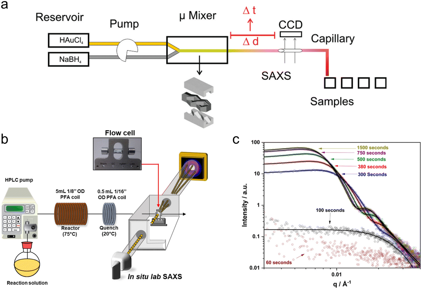 | ||
| Fig. 12 Laboratory-based X-ray scattering analysis. (a) A flow system for operando SAXS studies of the synthesis of gold nanoparticles. Different tubing lengths (Δd) between a commercial micro-mixer and the X-ray beam give access to different time points (used with permission from Polte et al., 2010; Copyright 2010 American Chemical Society).257 (b) A flow system for in situ SAXS studies of the polymerization-induced self-assembly comprising a heated reactor module and a cold-quench to stop the reaction before SAXS analysis. (c) Time-resolved SAXS data of nano-objects obtained with the system in (b) at reaction times controlled by the applied flow rate (adapted with permission from Guild et al. 2023; Copyright 2023 The Authors).268 | ||
A similar approach was later employed by Chen et al. and Herbst et al. to study the nucleation and growth of gold and ZnO NPs, respectively, over hours by simultaneous SAXS/WAXS and UV-vis spectroscopy.260,261 In contrast to Polte et al., once a steady flow was achieved within the capillary, flows were stopped and the reactions were followed within the static solutions. The authors analyzed the syntheses with a time resolution of between 0.5 and 10 minutes depending on the required acquisition time. Tillier et al. used a modified version of the electrochemical flow cell of Binninger et al. (reviewed in section 4.2.4) to study the degradation of carbon-supported Pt NP catalysts.262 Compared to their synchrotron experiments with exposure times on the second to minute time-scale, the acquisition of laboratory SAXS patterns with good signal-to-noise ratio required approximately 1 hour. Therefore, it is clear that depending on the kinetics of a reaction or process of interest, the experiment must be designed to consider the acquisition time required for lower flux laboratory sources.
García-Lojo et al. performed a synchrotron and laboratory SAXS study of the assembly of NPs into colloidal supercrystals by pervaporation in microfluidic channels.265 In comparing 2D SAXS data collected at the synchrotron and the laboratory, they observed that single-crystal small angle diffraction spots were much better resolved in the synchrotron data due to the smaller beam size and higher angular resolution. Finally, Ehm et al. 3D printed a millifluidic dialysis chamber with COC windows for monitoring 100 μL samples by SAXS.266 They demonstrated the device by following reversible structural transitions in lipids and polymers induced by changing media pH and salt concentration over hours using acquisition times of 20 min. The in situ laboratory SAXS data were compared to ex situ data collected using synchrotron radiation with good agreement.
Radajewski et al. performed a microfluidic SAXS study on a state-of-the-art laboratory SAXS platform that was modified to obtain a small 0.25 × 0.25 mm2 beam while providing a flux density of almost 107 photons s−1.267 In particular, they investigated the quality of data that could be obtained from flows of strongly scattering inorganic nanoparticles to moderately to weakly scattering proteins and polymer materials. For the high contrast gold and silica NPs studied, 10 min exposures were enough to obtain good quality SAXS patterns that could be fit with form and structure factors and for which the invariant could be calculated. For more weakly scattering bovine serum albumin (BSA) and latex NPs, longer 1 hour acquisitions were required to fit form factors, and even in these cases, increased noise especially at high q, made it difficult to resolve all the structure peaks of dilute samples. However, these results are very promising, especially for stronger contrast inorganic materials, and the use of a rotating anode or liquid metal jet source could provide between one and two orders of magnitude greater flux with the same optical configuration.
The second platform is the Flow-Xl National Facility for Analysis of Crystallization in Flow Systems located at the University of Leeds (UK).269 Flow-Xl is built around an X-ray diffractometer with a microfocused rotating anode source that is also coupled to a Raman spectrometer for performing simultaneous XRD/Raman. This facility was designed specifically for performing operando flow-based experiments, and as such, is equipped with a range of sample environments from millifluidic flow cells and humidity chambers to microfluidic devices. Commissioning experiments on this platform performed by Turner et al. demonstrated its potential for studying the nucleation and growth of inorganic and organic materials from aqueous solution.269 XRD and Raman yielded information on the dynamics of both the solid phases and solution chemistry, with limits of detection of 0.02–0.1 wt% and 0.625–2.5 g L−1, respectively, depending on the materials and solution species studied. For operando analysis of the cooling crystallization of NaSO4, XRD and Raman acquisition times of 18 and 17 s, respectively, were found to be sufficient to obtain data with good signal-to-noise ratio.
6.2 X-ray spectroscopy
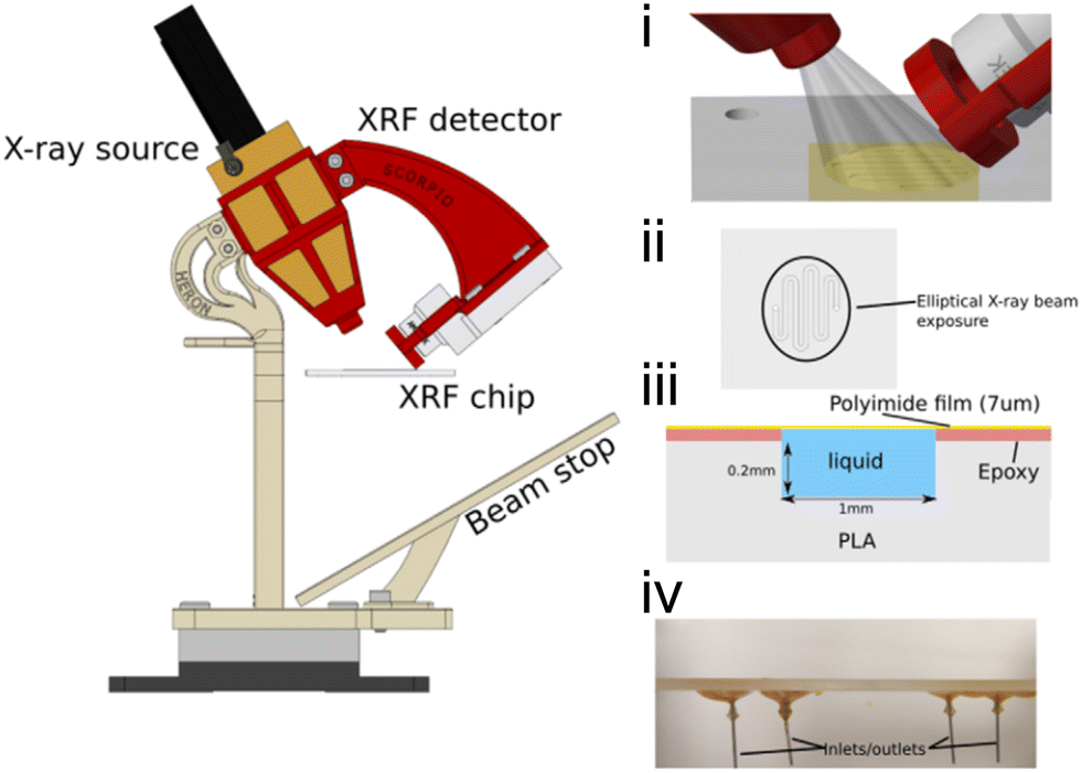 | ||
| Fig. 13 Experimental setup for laboratory-based X-ray fluorescence analysis (left). (i) View of the measurement area. (ii) Illustration of the microchannel path and the elliptical footprint of the X-ray beam. (iii) Cross-section of the microchannel. (iv) Photograph of the XRF device (used with permission from Maurice et al.; Copyright 2021 The Authors).272 | ||
6.3 X-ray imaging
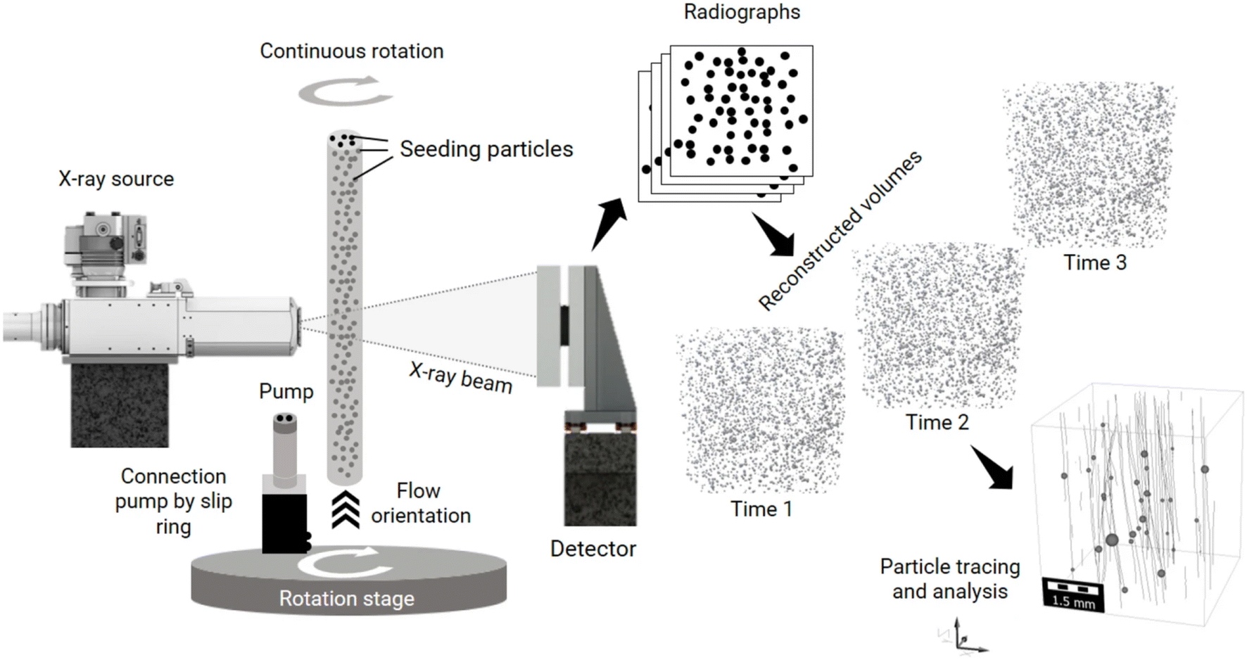 | ||
| Fig. 14 Experimental setup for laboratory-based 3D tomographic X-ray particle tracking velocimetry of a creeping millifluidic flow (used with permission from Mäkiharju et al.; Copyright 2021 The Authors.283 | ||
7 Discussion and outlook
The numerous examples cited in this review demonstrate the huge interest in using micro/millifluidics to carry out in situ and operando X-ray analyzes in both liquids and gases. We have seen that there is interest across all types of X-ray analysis, whether scattering, spectroscopy, or imaging and using both synchrotron and laboratory sources. In total, we have reviewed 148 articles (139 explicitly found in Tables 1–4), which we believe represents a near-comprehensive account of micro- and milli-fluidic X-ray literature in the physical sciences from the year 1999 until 2023. The growth in the number of articles produced is clear (Fig. 15), where the average number of papers produced per year from 1999 to 2015 was ∼4 and the number per year since the life sciences review of Ghazal et al.12 in 2016 is ∼10.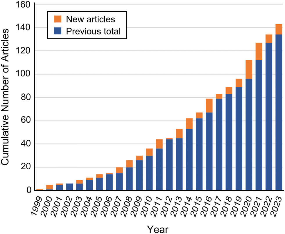 | ||
| Fig. 15 Chronology of the articles covered in this review (excluding articles from 2024). | ||
There is good reason for this high and growing level of interest. Specifically for continuous flow devices, the renewal of fluid under the beam has several advantages for X-ray measurements, including increasing their temporal resolution. In continuous flow, time resolution does not depend on the frame rate of a detector, but rather on the time it takes for fluid to pass through the beam and, therefore, on the linear velocity of the fluid as well as the beam size (and, in certain cases, on the initial mixing processes). Inline fluidic devices also make it possible to reduce the aging time of the sample before analysis by eliminating the step of introducing the sample under beam. This both reduces the observation dead time while guaranteeing the repeatability of measurements, e.g., by eliminating sample preparation artefacts. Using an inline fluidic configuration can also increase the rate at which samples can be measured thanks to the possibility of changing the nature of the sample (e.g., flow rate ratio, temperature) without a disassembly/reassembly operation, a particularly time-consuming process for techniques requiring operation under vacuum. This time saving makes it possible to accelerate data collection and even consider performing large screening studies. Finally, the continuous renewal of the sample under an ionizing beam limits the effects of radiation damage.
The size reduction associated with microfluidic devices adds further advantages to the previous list. It makes it possible to reduce the necessary sample volumes by one or more orders of magnitude, to carry out transmission analysis of highly absorbing samples (crucial in the soft X-ray domain), to access reaction times of less than a millisecond due to very efficient mixing functions at the micro-scale, and more generally, to combine many types of sample manipulation (e.g., droplet generation, separation, heating) into a single platform. It also results in an increase in the surface area-to-volume ratio, which can be a significant advantage when the objective is to probe the interactions between the substrate of the device and the objects conveyed by the flow, for instance, in catalysis studies. This increase of surface effects can, however, also constitute a point of weakness when uncontrolled events of adsorption and/or heterogeneous nucleation on the walls of a microchannel obscure or alter the bulk phenomena of interest.102
Initially condensing into a field of research in its own right,96 microfluidics quickly became a formidable tool for manipulating samples in domains as varied as biology, clinical diagnostics, synthetic chemistry, and materials science.83,84,300,301 Many research groups and companies have found success in applying microfluidic tools to these various areas. However, “going microfluidic” normally requires a large investment in equipment and technical skill, and this has been no different for groups looking to use fluidic devices for in situ X-ray analysis. In our opinion, perhaps the greatest bottleneck here has been in the complex microfabrication techniques and specific environments required for making conventional microfluidic devices. Such environments, of the “cleanroom” type, are characterized by a very low concentration of particles in the air as well as controlled temperature and relative humidity. Various specific equipment, such as spin-coaters, UV mask aligners, and plasma cleaners are also necessary. The investment, both in terms of cost and manpower, needed to establish such an environment cannot, therefore, be justified when its use is only occasional. This strongly hinders the uptake of microfluidics by non-specialist laboratories.
Fortunately, this barrier is continually being lowered due to the increasing availability of commercial solutions and the development of more accessible methods in microfabrication. Some companies (e.g., Microfluidic ChipShop, Micronit, Protochips) offer turnkey microfluidic devices associated with different fluidic functions such as droplet production, mixing, and electrochemistry. This solution thus relieves the user of any microfabrication duties and might only require access to a laminar flow hood to guarantee sufficient cleanliness when setting up the fluidic system. Indeed, many of the studies reviewed herein were performed with commercially available components or completely commercial chips, for example, ref. 160, 165 and 287 and several others.
At the same time, microfabrication is beginning to require less expertise due to new technologies that reduce the number of fabrication steps and guarantee very good device reproducibility and reliability. For photolithographic cleanroom-based fabrication, the use of commercial polymer films (i.e., dry film photoresists) of calibrated thickness for the creation of molds avoids the production of photoresist films by spin-coating, the result of which strongly depends on the temperature and humidity of the laboratory.302 Many non-cleanroom routes are also available. The use of hot embossable materials such as cyclic olefin copolymers (e.g., TOPAS®) or cyclic olefin polymers (e.g., ZEONOR®, ZEONEX®) makes it possible to replicate the same device many times in an automated and repeatable manner.303,304 The use of laser micromachining makes it possible to produce monolithic devices from many types of materials and/or to produce “sandwich”-type devices combining different materials, again in an automated manner.102,305,306 The main challenge with the high-performing femtosecond laser machining platforms required for patterning small features in a large range of materials is that their cost is on the scale of large cleanroom equipment. Much less expensive, 3D printing now makes it possible to directly print devices with minimum channel sizes below 100 μm using commercial printers with minimal to no modifications.125,307 Indeed, a large number of the studies used here were performed with 3D-printed components or chips (e.g., ref. 131, 216 and 266). Further, the adoption of simple plug-and-play millifluidic devices or millifluidic devices with lower requirements in manufacturing precision can still produce excellent data (see ref. 127, 262 and 273 for example). The multiplicity of available fabrication techniques now enables one to be more selective in the choice of device material to optimize key parameters such as its X-ray absorption or scattering profile or even its degradation under irradiation. For example, in our laboratory, where we perform a variety of different X-ray techniques for different types of samples, we have investigated every process mentioned above and found them all to be useful depending on the technique requirements and demands of the particular experiment.
These developments should ultimately encourage the use of micro- and milli-fluidic sample environments for in situ characterization at the synchrotron and in the laboratory. Until very recently, synchrotron studies conducted with microfluidic devices produced relatively little data due to the numerous technical challenges encountered during their implementation. Their handling, already delicate, is made even more difficult at the synchrotron and away from one's own laboratory environment. Consequently, journal publications only reflect a small part of the real effort made by the scientific community to develop micro- and milli-fluidic tools that better exploit the potential of X-ray analysis. For their part, synchrotron facilities have largely participated in this effort by developing microfocused beams compatible with the typical size of microfluidic channels (typically hundreds of microns). Many synchrotron facilities have also formed dedicated teams to help users with sample preparation in general, or microfluidics in particular, such as the Partnership for Soft Condensed Matter at the ESRF,125 the Microfluidic Laboratory at SOLEIL,227 and the Sample Environment Development Laboratory at Diamond Light Source.
Additional actions on their part could further facilitate micro- and milli-fluidic experiments. These include the installation of “clean” zones in the form of laminar flow hoods or biosafety cabinets (ISO 7 or 5)—essential for the preparation of the devices before experiments—near the beamline experimental hutch, the provision of commercial microfluidic environments already tested and integrated by the beamline staff, and the inclusion of inline optical microscopes for the visualization of microfluidic channels and the identification of measurement points. To our knowledge, automated or remote access to microfluidic equipment has not yet been implemented at a synchrotron beamline. However, this has been demonstrated for stopped-flow devices at bioSAXS beamlines (e.g., SSRL 4.2, PETRA III P12) and may be possible in the future for continuous flow micro- and milli-fluidic platforms for greater accessibility.
There are also several things beamline users can do to increase the success rate of their microfluidics beamtimes. The first is ensuring that the devices they bring are safe and reliable, e.g., not prone to leaking on expensive beamline hardware. Beamline staff have invested significant time in building their unique instruments and must continue to devote time to hosting user experiments. When users come with unreliable devices that do not produce data and thus, do not produce papers, they are less enthusiastic about recommending future microfluidics experiments. We have seen above that there are many routes to making robust micro- and milli-fluidic devices. We have also seen in section 6 that laboratory-based analysis is becoming more and more feasible. For this reason, we recommend that potential users try to perform an experiment with a laboratory instrument before applying for synchrotron beamtime. For example, the Sample Environment Development Laboratory at Diamond even offers this opportunity in partnership with beamline I22 and their offline SAXS platform.268 Even if an experiment is not feasible with the lower flux of a laboratory source, using a laboratory instrument to first characterize the scattering/absorption of a device such as done by Lange et al.92 or practicing the mounting of a device to avoid any potential surprises at a beamtime can go a long way.
X-ray analysis techniques, whether performed with a synchrotron or a laboratory source, are powerful tools for structural and chemical characterization. When combined with a micro- or milli-fluidic sample environment, they offer unparalleled possibilities for in situ and operando studies. The combination makes it possible, on one hand, to eliminate the preparation artifacts inherent in post-mortem analyses, and substantially improves, on the other hand, the temporal resolution compared to studies in a static configuration (i.e., without fluid renewal). However, while synchrotron light sources have long been and will continue to be a powerful tool in the arsenal of crystallographers and chemists, the relative inaccessibility of these facilities does limit the progress of individual research teams, which could otherwise measure more samples, develop more robust workflows, and iterate more rapidly. It is here we see tremendous potential for the current generation of commercial laboratory X-ray instruments, not just to permit more efficient use of synchrotron beamtime, but also to support completely independent in situ flow-based analysis platforms (see section 6.1.5).
Perhaps the most innovative prospect in the use of micro- and milli-fluidic X-ray sample environments is the possibility of exercising feedback control over the injected reagents, temperature, or other reaction conditions. Real-time analysis of data coupled with machine learning, as demonstrated by Fong et al.111 and Younes et al.112 for SAXS (section 3.2.3), makes it possible to direct the system towards a state corresponding to a pre-defined structural or chemical parameter. For example, in the field of (nano)materials synthesis, this ability should facilitate a departure from the classical trial-and-error approach and guarantee both the outcome of the syntheses and their reproducibility. Another recent study reported an autonomous laboratory for the high temperature synthesis of solid powders and their characterization by XRD.308 We could envision a similar type of system,309 but one using XRD/SAXS analysis for automated liquid phase synthesis with a micro- or milli-fluidic device benefiting from all of the advantages discussed above. The industrial value of such a paradigm shift would be considerable. Thus, making these techniques more accessible to the point of being routine, both at the synchrotron and in the laboratory, is a worthwhile effort not only for gaining fundamental scientific understanding, but also for developing new materials and processes for industrial and societal use.
Data availability
No primary research results, software or code have been included and no new data were generated or analysed as part of this review.Author contributions
MAL conceived the idea for the review and refined the concept in discussions with all authors. MAL performed the literature survey for sections 2, 3, 4, and 6. MAL and CC performed the literature survey for section 5. MAL wrote the manuscript with contributions from CC. MAL and CC edited the manuscript. FM, FT, and OT provided feedback in their areas of expertise.Conflicts of interest
There are no conflicts to declare.Acknowledgements
This work received state support managed by the French National Research Agency (ANR) under the France 2030 framework (ANR-22-PEXD-0006 and ANR-22-PEXD-0007). The authors would like to thank the many beamline scientists and staff who have supported their micro- and milli-fluidics beamtimes over the years, with a special mention of Sarah Day, Chiu Tang, Manfred Burghammer, Javier Perez, Thomas Bizien, Stefan Stanescu, Rachid Belkhou, Diego Pontoni, and Peter van der Linden. We also thank our editor, David Lake, for his assistance and patience during the preparation of the review.References
- J. J. De Yoreo, P. U. P. A. Gilbert, N. A. J. M. Sommerdijk, R. L. Penn, S. Whitelam, D. Joester, H. Zhang, J. D. Rimer, A. Navrotsky, J. F. Banfield, A. F. Wallace, F. M. Michel, F. C. Meldrum, H. Cölfen and P. M. Dove, Science, 2015, 349, aaa6760 CrossRef.
- A. E. S. Van Driessche, N. Van Gerven, P. H. H. Bomans, R. R. M. Joosten, H. Friedrich, D. Gil-Carton, N. Sommerdijk and M. Sleutel, Nature, 2018, 556, 89–94 CrossRef CAS.
- Z. Gao, M. Odstrcil, S. Böcklein, D. Palagin, M. Holler, D. F. Sanchez, F. Krumeich, A. Menzel, M. Stampanoni, G. Mestl, J. A. van Bokhoven, M. Guizar-Sicairos and J. Ihli, Sci. Adv., 2021, 7, eabf6971 CrossRef CAS.
- M. Macino, A. J. Barnes, S. M. Althahban, R. Qu, E. K. Gibson, D. J. Morgan, S. J. Freakley, N. Dimitratos, C. J. Kiely, X. Gao, A. M. Beale, D. Bethell, Q. He, M. Sankar and G. J. Hutchings, Nat. Catal., 2019, 2, 873–881 CrossRef CAS.
- D. P. Finegan, M. Scheel, J. B. Robinson, B. Tjaden, I. Hunt, T. J. Mason, J. Millichamp, M. Di Michiel, G. J. Offer, G. Hinds, D. J. L. Brett and P. R. Shearing, Nat. Commun., 2015, 6, 6924 CrossRef CAS.
- S. N. S. Hapuarachchi, Z. Sun and C. Yan, Adv. Sustainable Syst., 2018, 2, 1700182 CrossRef.
- Z. Ning, D. S. Jolly, G. Li, R. De Meyere, S. D. Pu, Y. Chen, J. Kasemchainan, J. Ihli, C. Gong, B. Liu, D. L. R. Melvin, A. Bonnin, O. Magdysyuk, P. Adamson, G. O. Hartley, C. W. Monroe, T. J. Marrow and P. G. Bruce, Nat. Mater., 2021, 20, 1121–1129 CrossRef CAS.
- D. H. Bilderback, P. Elleaume and E. Weckert, J. Phys. B, 2005, 38, S773 CrossRef CAS.
- H. Weise and W. Decking, presented in part at the 38th International Free Electron Laser Conference, FEL2017, Santa Fe, NM, USA, 2017 Search PubMed.
- S. Shin, AAPPS Bull., 2021, 31, 21 CrossRef.
- T. Skarzynski, Acta Crystallogr., Sect. D: Biol. Crystallogr., 2013, 69, 1283–1288 CrossRef CAS PubMed.
- A. Ghazal, J. P. Lafleur, K. Mortensen, J. P. Kutter, L. Arleth and G. V. Jensen, Lab Chip, 2016, 16, 4263–4295 RSC.
- M. A. Bañares, Catal. Today, 2005, 100, 71–77 CrossRef.
- M. Ilett, M. Afzali, B. Abdulkarim, Z. Aslam, S. Foster, M. Burgos-Ruiz, Y.-Y. Kim, F. C. Meldrum and R. M. Drummond-Brydson, J. Microsc., 2024, 1–14, DOI:10.1111/jmi.13300.
- M. A. Levenstein, K. Robertson, T. D. Turner, L. Hunter, C. O'Brien, C. O'Shaughnessy, A. N. Kulak, P. Le Magueres, J. Wojciechowski, O. O. Mykhaylyk, N. Kapur and F. C. Meldrum, IUCrJ, 2022, 9, 538–543 CrossRef CAS.
- C. L. Hansen, E. Skordalakes, J. M. Berger and S. R. Quake, Proc. Natl. Acad. Sci. U. S. A., 2002, 99, 16531–16536 CrossRef CAS.
- B. Zheng, J. D. Tice, L. S. Roach and R. F. Ismagilov, Angew. Chem., Int. Ed., 2004, 43, 2508–2511 CrossRef CAS.
- E. D. Greaves and A. Manz, Lab Chip, 2005, 5, 382–391 RSC.
- E. Lawrence Bright, C. Giacobbe and J. P. Wright, J. Synchrotron Radiat., 2021, 28, 1377–1385 CrossRef PubMed.
- U. Weierstall, Philos. Trans. R. Soc., B, 2014, 369, 20130337 CrossRef PubMed.
- S. Sui and S. L. Perry, Struct. Dyn., 2017, 4, 032202 CrossRef.
- L. Paulson, S. R. Narayanasamy, M. L. Shelby, M. Frank and M. Trebbin, Struct. Dyn., 2024, 11, 011101 CrossRef CAS.
- I. Grillo, Curr. Opin. Colloid Interface Sci., 2009, 14, 402–408 CrossRef CAS.
- J. T. Avaro, S. L. P. Wolf, K. Hauser and D. Gebauer, Angew. Chem., Int. Ed., 2020, 59, 6155–6159 CrossRef CAS PubMed.
- R. J. Clarke and M. A. A. Khalid, in Pumps, Channels, and Transporters, 2015, pp. 179–209, DOI:10.1002/9781119085126.ch7.
- O. L. J. Virtanen, M. Kather, J. Meyer-Kirschner, A. Melle, A. Radulescu, J. Viell, A. Mitsos, A. Pich and W. Richtering, ACS Omega, 2019, 4, 3690–3699 CrossRef CAS.
- S. Schmölzer, D. Gräbner, M. Gradzielski and T. Narayanan, Phys. Rev. Lett., 2002, 88, 258301 CrossRef.
- G. Guilera, M. A. Newton, C. Polli, S. Pascarelli, M. Guinó and K. K. Hii, Chem. Commun., 2006, 41, 4306–4308 RSC.
- B. Abécassis, F. Testard, O. Spalla and P. Barboux, Nano Lett., 2007, 7, 1723–1727 CrossRef PubMed.
- J. Polte, T. T. Ahner, F. Delissen, S. Sokolov, F. Emmerling, A. F. Thünemann and R. Kraehnert, J. Am. Chem. Soc., 2010, 132, 1296–1301 CrossRef CAS.
- T. M. Stawski, A. E. S. van Driessche, M. Ossorio, J. Diego Rodriguez-Blanco, R. Besselink and L. G. Benning, Nat. Commun., 2016, 7, 11177 CrossRef CAS PubMed.
- M. L. Whittaker, P. J. M. Smeets, H. Asayesh-Ardakani, R. Shahbazian-Yassar and D. Joester, Angew. Chem., Int. Ed., 2017, 56, 16028–16031 CrossRef CAS.
- J. Bolze, B. Peng, N. Dingenouts, P. Panine, T. Narayanan and M. Ballauff, Langmuir, 2002, 18, 8364–8369 CrossRef CAS.
- J. Cravillon, C. A. Schroder, R. Nayuk, J. Gummel, K. Huber and M. Wiebcke, Angew. Chem., Int. Ed., 2011, 50, 8067–8071 CrossRef CAS PubMed.
- F. Carraro, J. D. Williams, M. Linares-Moreau, C. Parise, W. Liang, H. Amenitsch, C. Doonan, C. O. Kappe and P. Falcaro, Angew. Chem., Int. Ed., 2020, 59, 8123 CrossRef CAS PubMed.
- M. J. Quayle, R. J. Davey, A. J. McDermott, G. J. T. Tiddy, D. T. Clarke and G. R. Jones, Phys. Chem. Chem. Phys., 2002, 4, 416–418 RSC.
- P. J. Chupas, K. W. Chapman, C. A. Kurtz, J. C. Hanson, P. L. Lee and C. P. Grey, J. Appl. Crystallogr., 2008, 41, 822–824 CrossRef CAS.
- C. G. Roessler, R. Agarwal, M. Allaire, R. Alonso-Mori, B. Andi, J. F. R. Bachega, M. Bommer, A. S. Brewster, M. C. Browne, R. Chatterjee, E. Cho, A. E. Cohen, M. Cowan, S. Datwani, V. L. Davidson, J. Defever, B. Eaton, R. Ellson, Y. Feng, L. P. Ghislain, J. M. Glownia, G. Han, J. Hattne, J. Hellmich, A. Héroux, M. Ibrahim, J. Kern, A. Kuczewski, H. T. Lemke, P. Liu, L. Majlof, W. M. McClintock, S. Myers, S. Nelsen, J. Olechno, A. M. Orville, N. K. Sauter, A. S. Soares, S. M. Soltis, H. Song, R. G. Stearns, R. Tran, Y. Tsai, M. Uervirojnangkoorn, C. M. Wilmot, V. Yachandra, J. Yano, E. T. Yukl, D. Zhu and A. Zouni, Structure, 2016, 24, 631–640 CrossRef CAS PubMed.
- R. H. Morris, E. R. Dye, D. Axford, M. I. Newton, J. H. Beale and P. T. Docker, Sci. Rep., 2019, 9, 12431 CrossRef CAS PubMed.
- B. Chance, Rev. Sci. Instrum., 1951, 22, 619–627 CrossRef CAS.
- R. L. Berger, B. Balko and H. F. Chapman, Rev. Sci. Instrum., 1968, 39, 493–498 CrossRef CAS PubMed.
- P. Panine, S. Finet, T. M. Weiss and T. Narayanan, Adv. Colloid Interface Sci., 2006, 127, 9–18 CrossRef CAS PubMed.
- L. Matthews and T. Narayanan, Colloid Polym. Sci., 2023, 301, 721–728 CrossRef CAS.
- A. Zabilska, A. H. Clark, D. Ferri, M. Nachtegaal, O. Kröcher and O. V. Safonova, Phys. Chem. Chem. Phys., 2022, 24, 21916–21926 RSC.
- C. K. Christensen, M. A. Karlsen, A. O. Drejer, B. P. Andersen, C. L. Jakobsen, M. Johansen, D. R. Sorensen, I. Kantor, M. R. V. Jorgensen and D. B. Ravnsbaek, J. Synchrotron Radiat., 2023, 30, 561–570 CrossRef CAS.
- P. Norby, Mater. Sci. Forum, 1996, 228–231, 147–152 CAS.
- R. Hodyss, T. H. Vu, M. Choukroun and M. L. Cable, J. Appl. Crystallogr., 2021, 54, 1268–1270 CrossRef CAS.
- B. S. Clausen, G. Steffensen, B. Fabius, J. Villadsen, R. Feidenhans'l and H. Topsøe, J. Catal., 1991, 132, 524–535 CrossRef CAS.
- P. Norby, J. Am. Chem. Soc., 1997, 119, 5215–5221 CrossRef CAS.
- K. M. O. Jensen, H. L. Andersen, C. Tyrsted, E. D. Bojesen, A. C. Dippel, N. Lock, S. J. L. Billinge, B. B. Iversen and M. Christensen, ACS Nano, 2014, 8, 10704–10714 CrossRef CAS PubMed.
- J. A. Rodriguez, X. Wang, P. Liu, W. Wen, J. C. Hanson, J. Hrbek, M. Pérez and J. Evans, Top. Catal., 2007, 44, 73–81 CrossRef CAS.
- T. R. Jensen, T. K. Nielsen, Y. Filinchuk, J.-E. Jorgensen, Y. Cerenius, E. M. Gray and C. J. Webb, J. Appl. Crystallogr., 2010, 43, 1456–1463 CrossRef CAS.
- N. V. Y. Scarlett, D. Hewish, R. Pattel and N. A. S. Webster, Rev. Sci. Instrum., 2017, 88, 105104 CrossRef PubMed.
- T.-D. Nguyen-Phan, Z. Liu, S. Luo, A. D. Gamalski, D. Vovchok, W. Xu, E. A. Stach, D. E. Polyansky, E. Fujita, J. A. Rodriguez and S. D. Senanayake, J. Phys. Chem. C, 2016, 120, 3472–3482 CrossRef CAS.
- J. Becker, M. Bremholm, C. Tyrsted, B. Pauw, K. M. O. Jensen, J. Eltzholt, M. Christensen and B. B. Iversen, J. Appl. Crystallogr., 2010, 43, 729–736 CrossRef CAS.
- P. Ferrer, I. da Silva, J. Rubio-Zuazo, B. F. Alfonso, C. Trobajo, S. Khainakov, J. R. Garcia, S. Garcia-Granda and G. R. Castro, J. Synchrotron Radiat., 2012, 19, 93–100 CrossRef CAS.
- H. N. Chapman, P. Fromme, A. Barty, T. A. White, R. A. Kirian, A. Aquila, M. S. Hunter, J. Schulz, D. P. DePonte, U. Weierstall, R. B. Doak, F. Maia, A. V. Martin, I. Schlichting, L. Lomb, N. Coppola, R. L. Shoeman, S. W. Epp, R. Hartmann, D. Rolles, A. Rudenko, L. Foucar, N. Kimmel, G. Weidenspointner, P. Holl, M. N. Liang, M. Barthelmess, C. Caleman, S. Boutet, M. J. Bogan, J. Krzywinski, C. Bostedt, S. Bajt, L. Gumprecht, B. Rudek, B. Erk, C. Schmidt, A. Homke, C. Reich, D. Pietschner, L. Struder, G. Hauser, H. Gorke, J. Ullrich, S. Herrmann, G. Schaller, F. Schopper, H. Soltau, K. U. Kuhnel, M. Messerschmidt, J. D. Bozek, S. P. Hau-Riege, M. Frank, C. Y. Hampton, R. G. Sierra, D. Starodub, G. J. Williams, J. Hajdu, N. Timneanu, M. M. Seibert, J. Andreasson, A. Rocker, O. Jonsson, M. Svenda, S. Stern, K. Nass, R. Andritschke, C. D. Schroter, F. Krasniqi, M. Bott, K. E. Schmidt, X. Y. Wang, I. Grotjohann, J. M. Holton, T. R. M. Barends, R. Neutze, S. Marchesini, R. Fromme, S. Schorb, D. Rupp, M. Adolph, T. Gorkhover, I. Andersson, H. Hirsemann, G. Potdevin, H. Graafsma, B. Nilsson and J. C. H. Spence, Nature, 2011, 470, U73–U81 CrossRef PubMed.
- D. P. DePonte, U. Weierstall, K. Schmidt, J. Warner, D. Starodub, J. C. H. Spence and R. B. Doak, J. Phys. D: Appl. Phys., 2008, 41, 195505 CrossRef.
- M. O. Wiedorn, D. Oberthur, R. Bean, R. Schubert, N. Werner, B. Abbey, M. Aepfelbacher, L. Adriano, A. Allahgholi, N. Al-Qudami, J. Andreasson, S. Aplin, S. Awel, K. Ayyer, S. Bajt, I. Barak, S. Bari, J. Bielecki, S. Botha, D. Boukhelef, W. Brehm, S. Brockhauser, I. Cheviakov, M. A. Coleman, F. Cruz-Mazo, C. Danilevski, C. Darmanin, R. B. Doak, M. Domaracky, K. Dorner, Y. Du, H. Fangohr, H. Fleckenstein, M. Frank, P. Fromme, A. M. Ganan-Calvo, Y. Gevorkov, K. Giewekemeyer, H. M. Ginn, H. Graafsma, R. Graceffa, D. Greiffenberg, L. Gumprecht, P. Gottlicher, J. Hajdu, S. Hauf, M. Heymann, S. Holmes, D. A. Horke, M. S. Hunter, S. Imlau, A. Kaukher, Y. Kim, A. Klyuev, J. Knoska, B. Kobe, M. Kuhn, C. Kupitz, J. Kuper, J. M. Lahey-Rudolph, T. Laurus, K. Le Cong, R. Letrun, P. L. Xavier, L. Maia, F. Maia, V. Mariani, M. Messerschmidt, M. Metz, D. Mezza, T. Michelat, G. Mills, D. C. F. Monteiro, A. Morgan, K. Muhlig, A. Munke, A. Munnich, J. Nette, K. A. Nugent, T. Nuguid, A. M. Orville, S. Pandey, G. Pena, P. Villanueva-Perez, J. Poehlsen, G. Previtali, L. Redecke, W. M. Riekehr, H. Rohde, A. Round, T. Safenreiter, I. Sarrou, T. Sato, M. Schmidt, B. Schmitt, R. Schonherr, J. Schulz, J. A. Sellberg, M. M. Seibert, C. Seuring, M. L. Shelby, R. L. Shoeman, M. Sikorski, A. Silenzi, C. A. Stan, X. T. Shi, S. Stern, J. Sztuk-Dambietz, J. Szuba, A. Tolstikova, M. Trebbin, U. Trunk, P. Vagovic, T. Ve, B. Weinhausen, T. A. White, K. Wrona, C. Xu, O. Yefanov, N. Zatsepin, J. G. Zhang, M. Perbandt, A. P. Mancuso, C. Betzel, H. Chapman and A. Barty, Nat. Commun., 2018, 9, 11 CrossRef PubMed.
- U. Weierstall, D. James, C. Wang, T. A. White, D. Wang, W. Liu, J. C. H. Spence, R. Bruce Doak, G. Nelson, P. Fromme, R. Fromme, I. Grotjohann, C. Kupitz, N. A. Zatsepin, H. Liu, S. Basu, D. Wacker, G. Won Han, V. Katritch, S. Boutet, M. Messerschmidt, G. J. Williams, J. E. Koglin, M. Marvin Seibert, M. Klinker, C. Gati, R. L. Shoeman, A. Barty, H. N. Chapman, R. A. Kirian, K. R. Beyerlein, R. C. Stevens, D. Li, S. T. A. Shah, N. Howe, M. Caffrey and V. Cherezov, Nat. Commun., 2014, 5, 3309 CrossRef.
- K. R. Beyerlein, H. O. Jönsson, R. Alonso-Mori, A. Aquila, S. Bajt, A. Barty, R. Bean, J. E. Koglin, M. Messerschmidt, D. Ragazzon, D. Sokaras, G. J. Williams, S. Hau-Riege, S. Boutet, H. N. Chapman, N. Tîmneanu and C. Caleman, Proc. Natl. Acad. Sci. U. S. A., 2018, 115, 5652–5657 CrossRef CAS.
- J. A. Sellberg, C. Huang, T. A. McQueen, N. D. Loh, H. Laksmono, D. Schlesinger, R. G. Sierra, D. Nordlund, C. Y. Hampton, D. Starodub, D. P. DePonte, M. Beye, C. Chen, A. V. Martin, A. Barty, K. T. Wikfeldt, T. M. Weiss, C. Caronna, J. Feldkamp, L. B. Skinner, M. M. Seibert, M. Messerschmidt, G. J. Williams, S. Boutet, L. G. M. Pettersson, M. J. Bogan and A. Nilsson, Nature, 2014, 510, 381–384 CrossRef CAS.
- H. Laksmono, T. A. McQueen, J. A. Sellberg, N. D. Loh, C. Huang, D. Schlesinger, R. G. Sierra, C. Y. Hampton, D. Nordlund, M. Beye, A. V. Martin, A. Barty, M. M. Seibert, M. Messerschmidt, G. J. Williams, S. Boutet, K. Amann-Winkel, T. Loerting, L. G. M. Pettersson, M. J. Bogan and A. Nilsson, J. Phys. Chem. Lett., 2015, 6, 2826–2832 CrossRef CAS PubMed.
- E. A. Schriber, D. W. Paley, R. Bolotovsky, D. J. Rosenberg, R. G. Sierra, A. Aquila, D. Mendez, F. Poitevin, J. P. Blaschke, A. Bhowmick, R. P. Kelly, M. Hunter, B. Hayes, D. C. Popple, M. Yeung, C. Pareja-Rivera, S. Lisova, K. Tono, M. Sugahara, S. Owada, T. Kuykendall, K. Yao, P. J. Schuck, D. Solis-Ibarra, N. K. Sauter, A. S. Brewster and J. N. Hohman, Nature, 2022, 601, 360–365 CrossRef CAS.
- F. Lehmkühler, F. Dallari, A. Jain, M. Sikorski, J. Möller, L. Frenzel, I. Lokteva, G. Mills, M. Walther, H. Sinn, F. Schulz, M. Dartsch, V. Markmann, R. Bean, Y. Kim, P. Vagovic, A. Madsen, P. Mancuso Adrian and G. Grübel, Proc. Natl. Acad. Sci. U. S. A., 2020, 117, 24110–24116 CrossRef.
- A. Aquila, M. S. Hunter, R. B. Doak, R. A. Kirian, P. Fromme, T. A. White, J. Andreasson, D. Arnlund, S. Bajt, T. R. M. Barends, M. Barthelmess, M. J. Bogan, C. Bostedt, H. Bottin, J. D. Bozek, C. Caleman, N. Coppola, J. Davidsson, D. P. DePonte, V. Elser, S. W. Epp, B. Erk, H. Fleckenstein, L. Foucar, M. Frank, R. Fromme, H. Graafsma, I. Grotjohann, L. Gumprecht, J. Hajdu, C. Y. Hampton, A. Hartmann, R. Hartmann, S. Hau-Riege, G. Hauser, H. Hirsemann, P. Holl, J. M. Holton, A. Hömke, L. Johansson, N. Kimmel, S. Kassemeyer, F. Krasniqi, K.-U. Kühnel, M. Liang, L. Lomb, E. Malmerberg, S. Marchesini, A. V. Martin, F. R. N. C. Maia, M. Messerschmidt, K. Nass, C. Reich, R. Neutze, D. Rolles, B. Rudek, A. Rudenko, I. Schlichting, C. Schmidt, K. E. Schmidt, J. Schulz, M. M. Seibert, R. L. Shoeman, R. Sierra, H. Soltau, D. Starodub, F. Stellato, S. Stern, L. Strüder, N. Timneanu, J. Ullrich, X. Wang, G. J. Williams, G. Weidenspointner, U. Weierstall, C. Wunderer, A. Barty, J. C. H. Spence and H. N. Chapman, Opt. Express, 2012, 20, 2706–2716 CrossRef CAS PubMed.
- V. Panneels, W. T. Wu, C. J. Tsai, P. Nogly, J. Rheinberger, K. Jaeger, G. Cicchetti, C. Gati, L. M. Kick, L. Sala, G. Capitani, C. Milne, C. Padeste, B. Pedrini, X. D. Li, J. Standfuss, R. Abela and G. Schertler, Struct. Dyn., 2015, 2, 8 CrossRef.
- M. Schmidt, Adv. Condens. Matter Phys., 2013, 10, DOI:10.1155/2013/167276.
- G. D. Calvey, A. M. Katz and L. Pollack, Anal. Chem., 2019, 91, 7139–7144 CrossRef CAS PubMed.
- J. R. Stagno, Y. Liu, Y. R. Bhandari, C. E. Conrad, S. Panja, M. Swain, L. Fan, G. Nelson, C. Li, D. R. Wendel, T. A. White, J. D. Coe, M. O. Wiedorn, J. Knoska, D. Oberthuer, R. A. Tuckey, P. Yu, M. Dyba, S. G. Tarasov, U. Weierstall, T. D. Grant, C. D. Schwieters, J. Zhang, A. R. Ferre-D'Amare, P. Fromme, D. E. Draper, M. Liang, M. S. Hunter, S. Boutet, K. Tan, X. Zuo, X. Ji, A. Barty, N. A. Zatsepin, H. N. Chapman, J. C. H. Spence, S. A. Woodson and Y. X. Wang, Nature, 2017, 541, 242–246 CrossRef CAS.
- J. L. Olmos, S. Pandey, J. M. Martin-Garcia, G. Calvey, A. Katz, J. Knoska, C. Kupitz, M. S. Hunter, M. Liang, D. Oberthuer, O. Yefanov, M. Wiedorn, M. Heyman, M. Holl, K. Pande, A. Barty, M. D. Miller, S. Stern, S. Roy-Chowdhury, J. Coe, N. Nagaratnam, J. Zook, J. Verburgt, T. Norwood, I. Poudyal, D. Xu, J. Koglin, M. H. Seaberg, Y. Zhao, S. Bajt, T. Grant, V. Mariani, G. Nelson, G. Subramanian, E. Bae, R. Fromme, R. Fung, P. Schwander, M. Frank, T. A. White, U. Weierstall, N. Zatsepin, J. Spence, P. Fromme, H. N. Chapman, L. Pollack, L. Tremblay, A. Ourmazd, G. N. Phillips and M. Schmidt, BMC Biol., 2018, 16, 59 CrossRef.
- M. Dasgupta, D. Budday, S. H. P. de Oliveira, P. Madzelan, D. Marchany-Rivera, J. Seravalli, B. Hayes, R. G. Sierra, S. Boutet, M. S. Hunter, R. Alonso-Mori, A. Batyuk, J. Wierman, A. Lyubimov, A. S. Brewster, N. K. Sauter, G. A. Applegate, V. K. Tiwari, D. B. Berkowitz, M. C. Thompson, A. E. Cohen, J. S. Fraser, M. E. Wall, H. van den Bedem and M. A. Wilson, Proc. Natl. Acad. Sci. U. S. A., 2019, 116, 25634 CrossRef CAS PubMed.
- K. R. Beyerlein, D. Dierksmeyer, V. Mariani, M. Kuhn, I. Sarrou, A. Ottaviano, S. Awel, J. Knoska, S. Fuglerud, O. Jonsson, S. Stern, M. O. Wiedorn, O. Yefanov, L. Adriano, R. Bean, A. Burkhardt, P. Fischer, M. Heymann, D. A. Horke, K. E. J. Jungnickel, E. Kovaleva, O. Lorbeer, M. Metz, J. Meyer, A. Morgan, K. Pande, S. Panneerselvam, C. Seuring, A. Tolstikova, J. Lieske, S. Aplin, M. Roessle, T. A. White, H. N. Chapman, A. Meents and D. Oberthuer, IUCrJ, 2017, 4, 769–777 CrossRef CAS PubMed.
- R. Dimper, H. Reichert, P. Raimondi, L. Sánchez Ortiz, F. Sette and J. Susini, ESRF Upgrade Programme Phase II (2015-2022) - Technical Design Study (“The Orange Book”), The European Synchrotron Radiation Facility Search PubMed.
- A. Meents, M. O. Wiedorn, V. Srajer, R. Henning, I. Sarrou, J. Bergtholdt, M. Barthelmess, P. Y. A. Reinke, D. Dierksmeyer, A. Tolstikova, S. Schaible, M. Messerschmidt, C. M. Ogata, D. J. Kissick, M. H. Taft, D. J. Manstein, J. Lieske, D. Oberthuer, R. F. Fischetti and H. N. Chapman, Nat. Commun., 2017, 8, 12 CrossRef PubMed.
- P. Nogly, D. James, D. J. Wang, T. A. White, N. Zatsepin, A. Shilova, G. Nelson, H. G. Liu, L. Johansson, M. Heymann, K. Jaeger, M. Metz, C. Wickstrand, W. T. Wu, P. Bath, P. Berntsen, D. Oberthuer, V. Panneels, V. Cherezov, H. Chapman, G. Schertler, R. Neutze, J. Spence, I. Moraes, M. Burghammer, J. Standfuss and U. Weierstall, IUCrJ, 2015, 2, 168–176 CrossRef CAS PubMed.
- O. Saldanha, M. E. Brennich, M. Burghammer, H. Herrmann and S. Köster, Biomicrofluidics, 2016, 10, 024108 CrossRef.
- S. E. Wolf, J. Leiterer, M. Kappl, F. Emmerling and W. Tremel, J. Am. Chem. Soc., 2008, 130, 12342–12347 CrossRef CAS PubMed.
- P. Sonderby, C. Soderberg, C. G. Frankaer, G. Peters, J. T. Bukrinski, A. Labrador, T. S. Plivelic and P. Harris, J. Synchrotron Radiat., 2020, 27, 396–404 CrossRef.
- A. M. Seddon, S. J. Richardson, K. Rastogi, T. S. Plivelic, A. M. Squires and C. Pfrang, J. Phys. Chem. Lett., 2016, 7, 1341–1345 CrossRef CAS.
- A. Milsom, A. M. Squires, J. A. Boswell, N. J. Terrill, A. D. Ward and C. Pfrang, Atmos. Chem. Phys., 2021, 21, 15003–15021 CrossRef CAS.
- A. J. deMello, Nature, 2006, 442, 394–402 CrossRef CAS.
- Y. Liu and X. Jiang, Lab Chip, 2017, 17, 3960–3978 RSC.
- A. B. Theberge, F. Courtois, Y. Schaerli, M. Fischlechner, C. Abell, F. Hollfelder and W. T. S. Huck, Angew. Chem., Int. Ed., 2010, 49, 5846–5868 CrossRef CAS.
- S. Köster and T. Pfohl, Mod. Phys. Lett. B, 2012, 26, 1230018 CrossRef.
- H. Song, J. D. Tice and R. F. Ismagilov, Angew. Chem., Int. Ed., 2003, 42, 768–772 CrossRef CAS PubMed.
- B. M. Zwickl, W. E. Shanks, A. M. Jayich, C. Yang, A. C. Bleszynski Jayich, J. D. Thompson and J. G. E. Harris, Appl. Phys. Lett., 2008, 92, 103125 CrossRef.
- B. Weinhausen and S. Köster, Lab Chip, 2013, 13, 212–215 RSC.
- C. Gosse, S. Stanescu, J. Frederick, S. Lefrançois, A. Vecchiola, M. Moskura, S. Swaraj, R. Belkhou, B. Watts, P. Haltebourg, C. Blot, J. Daillant, P. Guenoun and C. Chevallard, Lab Chip, 2020, 20, 3213–3229 RSC.
- K. Dhouib, C. K. Malek, W. Pfleging, B. Gauthier-Manuel, R. Duffait, G. Thuillier, R. Ferrigno, L. Jacquamet, J. Ohana, J. L. Ferrer, A. Theobald-Dietrich, R. Giege, B. Lorber and C. Sauter, Lab Chip, 2009, 9, 1412–1421 RSC.
- M. E. Brennich, J. F. Nolting, C. Dammann, B. Noding, S. Bauch, H. Herrmann, T. Pfohl and S. Köster, Lab Chip, 2011, 11, 708–716 RSC.
- T. Lange, S. Charton, T. Bizien, F. Testard and F. Malloggi, Lab Chip, 2020, 20, 2990–3000 RSC.
- R. Barrett, M. Faucon, J. Lopez, G. Cristobal, F. Destremaut, A. Dodge, P. Guillot, P. Laval, C. Masselon and J. B. Salmon, Lab Chip, 2006, 6, 494–499 RSC.
- S. Sui, Y. X. Wang, K. W. Kolewe, V. Srajer, R. Henning, J. D. Schiffman, C. Dimitrakopoulos and S. L. Perry, Lab Chip, 2016, 16, 3082–3096 RSC.
- Z. Ren, M. Ayhan, S. Bandara, K. Bowatte, I. Kumarapperuma, S. Gunawardana, H. Shin, C. Wang, X. T. Zeng and X. J. Yang, Lab Chip, 2018, 18, 2246–2256 RSC.
- T. M. Squires and S. R. Quake, Rev. Mod. Phys., 2005, 77, 977–1026 CrossRef CAS.
- H. A. Stone, A. D. Stroock and A. Ajdari, Annu. Rev. Fluid Mech., 2004, 36, 381–411 CrossRef.
- Z. Lu, J. McMahon, H. Mohamed, D. Barnard, T. R. Shaikh, C. A. Mannella, T. Wagenknecht and T.-M. Lu, Sens. Actuators, B, 2010, 144, 301–309 CrossRef CAS.
- A. D. Stroock, S. K. W. Dertinger, A. Ajdari, I. Mezić, H. A. Stone and G. M. Whitesides, Science, 2002, 295, 647–651 CrossRef CAS.
- X. Casadevall i Solvas and A. deMello, Chem. Commun., 2011, 47, 1936–1942 RSC.
- O. Saldanha, R. Graceffa, C. Hemonnot, C. Ranke, G. Brehm, M. Liebi, B. Marmiroli, B. Weinhausen, M. Burghammer and S. Köster, ChemPhysChem, 2017, 18, 1220 CrossRef CAS PubMed.
- M. A. Levenstein, Y.-Y. Kim, L. Hunter, C. Anduix-Canto, C. González Niño, S. J. Day, S. Li, W. J. Marchant, P. A. Lee, C. C. Tang, M. Burghammer, F. C. Meldrum and N. Kapur, Lab Chip, 2020, 20, 2954–2964 RSC.
- B. Wunderlich, D. Nettels and B. Schuler, Lab Chip, 2014, 14, 219–228 RSC.
- B. D. Cullity and S. R. Stock, Elements of X-Ray Diffraction, Prentice Hall, New Jersey, 3rd edn, 2001 Search PubMed.
- P. Lindner and T. Zemb, Neutrons, X-rays and Light: Scattering Methods Applied to Soft Condensed Matter, North Holland, 2002 Search PubMed.
- A. Merlin, J. Angly, L. Daubersies, C. Madeira, S. Schoder, J. Leng and J. B. Salmon, Eur. Phys. J. E: Soft Matter Biol. Phys., 2011, 34, 1–7 CrossRef.
- L. C. McKenzie, P. M. Haben, S. D. Kevan and J. E. Hutchison, J. Phys. Chem. C, 2010, 114, 22055–22063 CrossRef CAS.
- M. Takesue, T. Tomura, M. Yamada, K. Hata, S. Kuwamoto and T. Yonezawa, J. Am. Chem. Soc., 2011, 133, 14164–14167 CrossRef CAS.
- R. Stehle, G. Goerigk, D. Wallacher, M. Ballauff and S. Seiffert, Lab Chip, 2013, 13, 1529–1537 RSC.
- I. Rodríguez-Ruiz, S. Charton, D. Radajewski, T. Bizien and S. Teychené, CrystEngComm, 2018, 20, 3302–3307 RSC.
- A. Y. Fong, L. Pellouchoud, M. Davidson, R. C. Walroth, C. Church, E. Tcareva, L. Wu, K. Peterson, B. Meredig and C. J. Tassone, J. Chem. Phys., 2021, 154, 224201 CrossRef CAS.
- K. Younes, M. Poli, P. Muhunthan, I. Rajkovic, S. Ermon, T. M. Weiss and M. Ihme, Nucl. Instrum. Methods Phys. Res., Sect. A, 2023, 1057, 168719 CrossRef CAS.
- J. F. Moulin, S. V. Roth and P. Müller-Buschbaum, Rev. Sci. Instrum., 2008, 79, 015109 CrossRef.
- E. Metwalli, J. F. Moulin, J. Perlich, W. Wang, A. Diethert, S. V. Roth and P. Müller-Buschbaum, Langmuir, 2009, 25, 11815–11821 CrossRef CAS PubMed.
- J. Kehres, T. Pedersen, F. Masini, J. W. Andreasen, M. M. Nielsen, A. Diaz, J. H. Nielsen, O. Hansen and I. Chorkendorff, J. Synchrotron Radiat., 2016, 23, 455–463 CrossRef CAS PubMed.
- H. G. Alison, R. J. Davey, J. Garside, M. J. Quayle, G. J. T. Tiddy, D. T. Clarke and G. R. Jones, Phys. Chem. Chem. Phys., 2003, 5, 4998–5000 RSC.
- T. Chen, A. Neville, K. Sorbie and Z. Zhong, Faraday Discuss., 2007, 136, 355–365 RSC.
- T. Chen, A. Neville, K. Sorbie and Z. Zhong, Chem. Eng. Sci., 2009, 64, 912–918 CrossRef CAS.
- E. Mavredaki, A. Neville and K. Sorbie, Appl. Surf. Sci., 2011, 257, 4264–4271 CrossRef CAS.
- D. Burkle, R. De Motte, W. Taleb, A. Kleppe, T. Comyn, S. M. Vargas, A. Neville and R. Barker, Rev. Sci. Instrum., 2016, 87, 7 CrossRef.
- T. Beuvier, E. A. C. Panduro, P. Kwasniewski, S. Marre, C. Lecoutre, Y. Garrabos, C. Aymonier, B. Calvignac and A. Gibaud, Lab Chip, 2015, 15, 2002–2008 RSC.
- M. A. Levenstein, C. Anduix-Canto, Y.-Y. Kim, M. A. Holden, C. González Niño, D. C. Green, S. E. Foster, A. N. Kulak, L. Govada, N. E. Chayen, S. J. Day, C. C. Tang, B. Weinhausen, M. Burghammer, N. Kapur and F. C. Meldrum, Adv. Funct. Mater., 2019, 29, 1808172 CrossRef.
- M. A. Levenstein, L. E. Wayment, C. D. Scott, R. A. Lunt, P.-B. Flandrin, S. Day, C. Tang, C. C. Wilson, F. C. Meldrum, N. Kapur and K. Robertson, Anal. Chem., 2020, 92, 7754–7761 CrossRef CAS PubMed.
- D. Radajewski, L. Hunter, X. He, O. Nahi, J. M. Galloway and F. C. Meldrum, Lab Chip, 2021, 21, 4498–4506 RSC.
- P. J. E. M. van der Linden, A. M. Popov and D. Pontoni, Lab Chip, 2020, 20, 4128–4140 RSC.
- B. Fleury, M.-A. Neouze, J.-M. Guigner, N. Menguy, O. Spalla, T. Gacoin and D. Carriere, ACS Nano, 2014, 8, 2602–2608 CrossRef CAS.
- M. O. Besenhard, A. P. LaGrow, A. Hodzic, M. Kriechbaum, L. Panariello, G. Bais, K. Loizou, S. Damilos, M. Margarida Cruz, N. T. K. Thanh and A. Gavriilidis, Chem. Eng. J., 2020, 399, 125740 CrossRef CAS.
- M. Durelle, F. Gobeaux, T. K. Truong, S. Charton and D. Carriere, Cryst. Growth Des., 2023, 23, 5631–5640 CrossRef CAS.
- M. W. Terban, D. Banerjee, S. Ghose, B. Medasani, A. Shukla, B. A. Legg, Y. Zhou, Z. Zhu, M. L. Sushko, J. J. De Yoreo, J. Liu, P. K. Thallapally and S. J. L. Billinge, Nanoscale, 2018, 10, 4291–4300 RSC.
- M. L. Beauvais, P. J. Chupas, D. O'Nolan, J. B. Parise and K. W. Chapman, ACS Mater. Lett., 2021, 3, 698–703 CrossRef CAS.
- M. L. Beauvais, B. A. Sanchez Monserrate, T. Feng, R. Chen, P. Liu, P. J. Chupas and K. W. Chapman, J. Appl. Crystallogr., 2022, 55, 258–264 CrossRef CAS.
- M. J. Young, N. M. Bedford, N. Jiang, D. Lin and L. Dai, J. Synchrotron Radiat., 2017, 24, 787–795 CrossRef CAS PubMed.
- G. Kwon, Y.-H. Cho, K.-B. Kim, J. D. Emery, I. S. Kim, X. Zhang, A. B. F. Martinson and D. M. Tiede, J. Synchrotron Radiat., 2019, 26, 1600–1611 CrossRef CAS PubMed.
- L. Pollack, M. W. Tate, N. C. Darnton, J. B. Knight, S. M. Gruner, W. A. Eaton and R. H. Austin, Proc. Natl. Acad. Sci. U. S. A., 1999, 96, 10115–10117 CrossRef CAS.
- L. Pollack, M. W. Tate, A. C. Finnefrock, C. Kalidas, S. Trotter, N. C. Darnton, L. Lurio, R. H. Austin, C. A. Batt, S. M. Gruner and S. G. J. Mochrie, Phys. Rev. Lett., 2001, 86, 4962–4965 CrossRef CAS PubMed.
- M. Jiang and R. D. Braatz, CrystEngComm, 2019, 21, 3534–3551 RSC.
- M. O. Besenhard, S. Pal, G. Gkogkos and A. Gavriilidis, React. Chem. Eng., 2023, 8, 955–977 RSC.
- K. Robertson, P. B. Flandrin, A. R. Klapwijk and C. C. Wilson, Cryst. Growth Des., 2016, 16, 4759–4764 CrossRef CAS.
- V. Körstgens, M. Philipp, D. Magerl, M. A. Niedermeier, G. Santoro, S. V. Roth and P. Müller-Buschbaum, RSC Adv., 2014, 4, 1476–1479 RSC.
- J. Han, F. Testard, F. Malloggi, C. Pierre-Eugene, N. Menguy and O. Spalla, Langmuir, 2012, 28, 15966–15974 CrossRef PubMed.
- R. K. Ramamoorthy, E. Yildirim, E. Barba, P. Roblin, J. A. Vargas, L.-M. Lacroix, I. Rodriguez-Ruiz, P. Decorse, V. Petkov, S. Teychené and G. Viau, Nanoscale, 2020, 12, 16173–16188 RSC.
- B. He, L. K. Macreadie, J. Gardiner, S. G. Telfer and M. R. Hill, ACS Appl. Mater. Interfaces, 2021, 13, 54284–54293 CrossRef CAS.
- X. Chen, J. Wang, R. Pan, S. Roth and S. Förster, J. Phys. Chem. C, 2021, 125, 1087–1095 CrossRef CAS.
- S. J. L. Billinge and M. G. Kanatzidis, Chem. Commun., 2004, 749–760, 10.1039/b309577k.
- B. Winter, Nucl. Instrum. Methods Phys. Res., Sect. A, 2009, 601, 139–150 CrossRef CAS.
- A. Iglesias-Juez, G. L. Chiarello, G. S. Patience and M. O. Guerrero-Pérez, Can. J. Chem. Eng., 2022, 100, 3–22 CrossRef CAS.
- O. Proux, E. Lahera, W. Del Net, I. Kieffer, M. Rovezzi, D. Testemale, M. Irar, S. Thomas, A. Aguilar-Tapia, E. F. Bazarkina, A. Prat, M. Tella, M. Auffan, J. Rose and J.-L. Hazemann, J. Environ. Qual., 2017, 46, 1146–1157 CrossRef CAS PubMed.
- M. A. Newton, A. J. Dent and J. Evans, Chem. Soc. Rev., 2002, 31, 83–95 RSC.
- K. Amemiya, K. Sakata and M. Suzuki-Sakamaki, Rev. Sci. Instrum., 2020, 91, 093104 CrossRef CAS.
- B. Detlefs, S. Graziano and P. Glatzel, Anal. Chem., 2023, 95, 8758–8762 CrossRef CAS.
- M. C. Ringo, M. S. Huhta, G. Shea-McCarthy, J. E. Penner-Hahn and C. E. Evans, Nucl. Instrum. Methods Phys. Res., Sect. B, 1999, 149, 177–181 CrossRef CAS.
- S. E. Mann, M. C. Ringo, G. Shea-McCarthy, J. Penner-Hahn and C. E. Evans, Anal. Chem., 2000, 72, 1754–1758 CrossRef CAS PubMed.
- M. M. Hoffmann, J. G. Darab, S. M. Heald, C. R. Yonker and J. L. Fulton, Chem. Geol., 2000, 167, 89–103 CrossRef CAS.
- M. M. Hoffmann, J. G. Darab and J. L. Fulton, Rev. Sci. Instrum., 2001, 105, 6876–6885 CAS.
- G. Sankar, E. Cao and A. Gavriilidis, Catal. Today, 2007, 125, 24–28 CrossRef CAS.
- E. M. Chan, M. A. Marcus, S. Fakra, M. ElNaggar, R. A. Mathies and A. P. Alivisatos, J. Phys. Chem. A, 2007, 111, 12210–12215 CrossRef CAS.
- G. Hofmann, G. Tofighi, G. Rinke, S. Baier, A. Ewinger, A. Urban, A. Wenka, S. Heideker, A. Jahn, R. Dittmeyer and J. D. Grunwaldt, J. Phys.: Conf. Ser., 2016, 712, 012072 CrossRef.
- G. Tofighi, H. Lichtenberg, J. Pesek, T. L. Sheppard, W. Wang, L. Schöttner, G. Rinke, R. Dittmeyer and J.-D. Grunwaldt, React. Chem. Eng., 2017, 2, 876–884 RSC.
- P. Micheal Raj, L. Barbe, M. Andersson, M. De Albuquerque Moreira, D. Haase, J. Wootton, S. Nehzati, A. E. Terry, R. J. Friel, M. Tenje and K. G. V. Sigfridsson Clauss, RSC Adv., 2021, 11, 29859–29869 RSC.
- S. Britto, C. M. A. Parlett, S. Bartlett, J. D. Elliott, K. Ignatyev and S. L. M. Schroeder, J. Phys. Chem. C, 2023, 127, 8631–8639 CrossRef CAS.
- S. Zinoveva, R. De Silva, R. D. Louis, P. Datta, C. S. S. R. Kumar, J. Goettert and J. Hormes, Nucl. Instrum. Methods Phys. Res., Sect. A, 2007, 582, 239–241 CrossRef CAS.
- H. Oyanagi, Z. H. Sun, Y. Jiang, M. Uehara, H. Nakamura, K. Yamashita, L. Zhang, C. Lee, A. Fukano and H. Maeda, J. Synchrotron Radiat., 2011, 18, 272–279 CrossRef CAS.
- J. Monnier, L. Legrand, L. Bellot-Gurlet, E. Foy, S. Reguer, E. Rocca, P. Dillmann, D. Neff, F. Mirambet, S. Perrin and I. Guillot, J. Nucl. Mater., 2008, 379, 105–111 CrossRef CAS.
- J. Monnier, S. Réguer, E. Foy, D. Testemale, F. Mirambet, M. Saheb, P. Dillmann and I. Guillot, Corros. Sci., 2014, 78, 293–303 CrossRef CAS.
- K. S. Krishna, C. V. Navin, S. Biswas, V. Singh, K. Ham, G. L. Bovenkamp, C. S. Theegala, J. T. Miller, J. J. Spivey and C. S. S. R. Kumar, J. Am. Chem. Soc., 2013, 135, 5450–5456 CrossRef PubMed.
- A. V. Dobrovolskaya, S. V. Chapek, O. A. Usoltsev, E. Naranov, D. N. Gorbunov, A. L. Trigub, A. L. Maximov, A. V. Soldatov and A. L. Bugaev, J. Phys. Chem. C, 2023, 127, 20727–20733 CrossRef CAS.
- J. L. Fulton, Y. Chen, S. M. Heald and M. Balasubramanian, Rev. Sci. Instrum., 2004, 75, 5228–5231 CrossRef CAS.
- O. Fuchs, F. Maier, L. Weinhardt, M. Weigand, M. Blum, M. Zharnikov, J. Denlinger, M. Grunze, C. Heske and E. Umbach, Nucl. Instrum. Methods Phys. Res., Sect. A, 2008, 585, 172–177 CrossRef CAS.
- M. Nagasaka, T. Hatsui, T. Horigome, Y. Hamamura and N. Kosugi, J. Electron Spectrosc. Relat. Phenom., 2010, 177, 130–134 CrossRef CAS.
- S. Schreck, G. Gavrila, C. Weniger and P. Wernet, Rev. Sci. Instrum., 2011, 82, 103101 CrossRef.
- J. Probst, C. N. Borca, M. A. Newton, J. van Bokhoven, T. Huthwelker, S. Stavrakis and A. deMello, ACS Meas. Sci. Au, 2021, 1, 27–34 CrossRef CAS.
- J. Brenker, K. Henzler, C. N. Borca, T. Huthwelker and T. Alan, Lab Chip, 2022, 22, 1214–1230 RSC.
- G. L. Chiarello, M. Nachtegaal, V. Marchionni, L. Quaroni and D. Ferri, Rev. Sci. Instrum., 2014, 85, 074102 CrossRef.
- E. K. Dann, E. K. Gibson, C. R. A. Catlow, V. Celorrio, P. Collier, T. Eralp, M. Amboage, C. Hardacre, C. Stere, A. Kroner, A. Raj, S. Rogers, A. Goguet and P. P. Wells, J. Catal., 2019, 373, 201–208 CrossRef CAS.
- B. Venezia, E. Cao, S. K. Matam, C. Waldron, G. Cibin, E. K. Gibson, S. Golunski, P. P. Wells, I. Silverwood, C. R. A. Catlow, G. Sankar and A. Gavriilidis, Catal. Sci. Technol., 2020, 10, 7842–7856 RSC.
- D. A. Huyke, A. Ramachandran, O. Ramirez-Neri, J. A. Guerrero-Cruz, L. B. Gee, A. Braun, D. Sokaras, B. Garcia-Estrada, E. I. Solomon, B. Hedman, M. U. Delgado-Jaime, D. P. DePonte, T. Kroll and J. G. Santiago, J. Synchrotron Radiat., 2021, 28, 1100–1113 CrossRef CAS.
- A. M. Karim, N. Al Hasan, S. Ivanov, S. Siefert, R. T. Kelly, N. G. Hallfors, A. Benavidez, L. Kovarik, A. Jenkins, R. E. Winans and A. K. Datye, J. Phys. Chem. C, 2015, 119, 13257–13267 CrossRef.
- T. Binninger, E. Fabbri, A. Patru, M. Garganourakis, J. Han, D. F. Abbott, O. Sereda, R. Kötz, A. Menzel, M. Nachtegaal and T. J. Schmidt, J. Electrochem. Soc., 2016, 163, H906 CrossRef CAS.
- R. K. Ramamoorthy, E. Yildirim, I. Rodriguez-Ruiz, P. Roblin, L.-M. Lacroix, A. Diaz, R. Parmar, S. Teychené and G. Viau, Lab Chip, 2024, 24, 327–338 RSC.
- S. Busch, T. H. Jensen, Y. Chushkin and A. Fluerasu, Eur. Phys. J. E: Soft Matter Biol. Phys., 2008, 26, 55–62 CrossRef CAS.
- A. Fluerasu, A. Moussaid, P. Falus, H. Gleyzolle and A. Madsen, J. Synchrotron Radiat., 2008, 15, 378–384 CrossRef CAS PubMed.
- A. Fluerasu, P. Kwasniewski, C. Caronna, F. Destremaut, J.-B. Salmon and A. Madsen, New J. Phys., 2010, 12, 035023 CrossRef.
- R. Urbani, F. Westermeier, B. Banusch, M. Sprung and T. Pfohl, J. Synchrotron Radiat., 2016, 23, 1401–1408 CrossRef CAS PubMed.
- J. R. M. Lhermitte, M. C. Rogers, S. Manet and M. Sutton, Rev. Sci. Instrum., 2017, 88, 015112 CrossRef PubMed.
- H.-G. Steinrück, C. J. Takacs, H.-K. Kim, D. G. Mackanic, B. Holladay, C. Cao, S. Narayanan, E. M. Dufresne, Y. Chushkin, B. Ruta, F. Zontone, J. Will, O. Borodin, S. K. Sinha, V. Srinivasan and M. F. Toney, Energy Environ. Sci., 2020, 13, 4312–4321 RSC.
- P. Muhunthan, H. Li, G. Vignat, E. R. Toro, K. Younes, Y. Sun, D. Sokaras, T. Weiss, I. Rajkovic, T. Osaka, I. Inoue, S. Song, T. Sato, D. Zhu, J. L. Fulton and M. Ihme, Rev. Sci. Instrum., 2024, 95, 013901 CrossRef CAS PubMed.
- R. L. Leheny, Curr. Opin. Colloid Interface Sci., 2012, 17, 3–12 CrossRef CAS.
- O. Shpyrko, J. Synchrotron Radiat., 2014, 21, 1057–1064 CrossRef CAS PubMed.
- A. Sakdinawat and D. Attwood, Nat. Photonics, 2010, 4, 840–848 CrossRef CAS.
- F. Pfeiffer, Nat. Photonics, 2018, 12, 9–17 CrossRef CAS.
- M. Endrizzi, Nucl. Instrum. Methods Phys. Res., Sect. A, 2018, 878, 88–98 CrossRef CAS.
- P. J. Withers, C. Bouman, S. Carmignato, V. Cnudde, D. Grimaldi, C. K. Hagen, E. Maire, M. Manley, A. Du Plessis and S. R. Stock, Nat. Rev. Methods Primers, 2021, 1, 18 CrossRef CAS.
- U. Neuhausler, C. Jacobsen, D. Schulze, D. Stott and S. Abend, J. Synchrotron Radiat., 2000, 7, 110–112 CrossRef CAS PubMed.
- J. Rieger, J. Thieme and C. Schmidt, Langmuir, 2000, 16, 8300–8305 CrossRef CAS.
- D. Guay, J. Stewart-Ornstein, X. Zhang and A. P. Hitchcock, Anal. Chem., 2005, 77, 3479–3487 CrossRef CAS.
- I. J. Drake, T. C. N. Liu, M. Gilles, T. Tyliszczak, A. L. D. Kilcoyne, D. K. Shuh, R. A. Mathies and A. T. Bell, Rev. Sci. Instrum., 2004, 75, 3242–3247 CrossRef CAS.
- T. Huthwelker, V. Zelenay, M. Birrer, A. Krepelova, J. Raabe, G. Tzvetkov, M. G. C. Vernooij and M. Ammann, Rev. Sci. Instrum., 2010, 81, 113706 CrossRef CAS.
- V. Zelenay, M. Ammann, A. Křepelová, M. Birrer, G. Tzvetkov, M. G. C. Vernooij, J. Raabe and T. Huthwelker, J. Aerosol Sci., 2011, 42, 38–51 CrossRef CAS.
- S. T. Kelly, P. Nigge, S. Prakash, A. Laskin, B. Wang, T. Tyliszczak, S. R. Leone and M. K. Gilles, Rev. Sci. Instrum., 2013, 84, 073708 CrossRef.
- E. de Smit, I. Swart, J. F. Creemer, G. H. Hoveling, M. K. Gilles, T. Tyliszczak, P. J. Kooyman, H. W. Zandbergen, C. Morin, B. M. Weckhuysen and F. M. F. de Groot, Nature, 2008, 456, 222–225 CrossRef CAS.
- E. de Smit, I. Swart, J. F. Creemer, C. Karunakaran, D. Bertwistle, H. W. Zandbergen, F. M. F. de Groot and B. M. Weckhuysen, Angew. Chem., Int. Ed., 2009, 48, 3632–3636 CrossRef CAS.
- M. Yoo, Y.-S. Yu, H. Ha, S. Lee, J.-S. Choi, S. Oh, E. Kang, H. Choi, H. An, K.-S. Lee, J. Y. Park, R. Celestre, M. A. Marcus, K. Nowrouzi, D. Taube, D. A. Shapiro, W. Jung, C. Kim and H. Y. Kim, Energy Environ. Sci., 2020, 13, 1231–1239 RSC.
- Y. Sun and Y. Wang, Nano Lett., 2011, 11, 4386–4392 CrossRef CAS.
- J. Lim, Y. Li, D. H. Alsem, H. So, S. C. Lee, P. Bai, D. A. Cogswell, X. Liu, N. Jin, Y.-s. Yu, N. J. Salmon, D. A. Shapiro, M. Z. Bazant, T. Tyliszczak and W. C. Chueh, Science, 2016, 353, 566–571 CrossRef CAS PubMed.
- T. Mefford, K. Karki, D. H. Alsem, D. Shapiro, N. Salmon and W. C. Chueh, Microsc. Microanal., 2019, 25, 2094–2095 CrossRef.
- J. T. Mefford, A. R. Akbashev, M. Kang, C. L. Bentley, W. E. Gent, H. D. Deng, D. H. Alsem, Y.-S. Yu, N. J. Salmon, D. A. Shapiro, P. R. Unwin and W. C. Chueh, Nature, 2021, 593, 67–73 CrossRef CAS.
- T. Ohigashi, M. Nagasaka, T. Horigome, N. Kosugi, S. M. Rosendahl and A. P. Hitchcock, AIP Conf. Proc., 2016, 1741, 050002 CrossRef.
- V. Prabu, M. Obst, H. Hosseinkhannazer, M. Reynolds, S. Rosendahl, J. Wang and A. P. Hitchcock, Rev. Sci. Instrum., 2018, 89, 063702 CrossRef PubMed.
- S.-J. Lee and G.-B. Kim, J. Appl. Phys., 2003, 94, 3620–3623 CrossRef CAS.
- W.-K. Lee, K. Fezzaa and T. Uemura, J. Synchrotron Radiat., 2011, 18, 302–304 CrossRef.
- M. Prodanović, W. B. Lindquist and R. S. Seright, J. Colloid Interface Sci., 2006, 298, 282–297 CrossRef.
- C. Noiriel, B. Madé and P. Gouze, Water Resour. Res., 2007, 43 DOI:10.1029/2006WR005379.
- S. Berg, H. Ott, S. A. Klapp, A. Schwing, R. Neiteler, N. Brussee, A. Makurat, L. Leu, F. Enzmann, J.-O. Schwarz, M. Kersten, S. Irvine and M. Stampanoni, Proc. Natl. Acad. Sci. U. S. A., 2013, 110, 3755–3759 CrossRef CAS.
- R. T. Armstrong, H. Ott, A. Georgiadis, M. Rücker, A. Schwing and S. Berg, Water Resour. Res., 2014, 50, 9162–9176 CrossRef.
- S. Hasan, V. Niasar, N. K. Karadimitriou, J. R. A. Godinho, N. T. Vo, S. An, A. Rabbani and H. Steeb, Proc. Natl. Acad. Sci. U. S. A., 2020, 117, 23443–23449 CrossRef CAS.
- A. Piovesan, T. Van De Looverbosch, P. Verboven, C. Achille, C. Parra Cabrera, E. Boller, Y. Cheng, R. Ameloot and B. Nicolai, Lab Chip, 2020, 20, 2403–2411 RSC.
- K. J. Dobson, S. B. Coban, S. A. McDonald, J. N. Walsh, R. C. Atwood and P. J. Withers, Solid Earth, 2016, 7, 1059–1073 CrossRef.
- T. Bultreys, S. Ellman, C. M. Schlepütz, M. N. Boone, G. K. Pakkaner, S. Wang, M. Borji, S. Van Offenwert, N. Moazami Goudarzi, W. Goethals, C. W. Winardhi and V. Cnudde, Proc. Natl. Acad. Sci. U. S. A., 2024, 121, e2316723121 CrossRef CAS.
- J. Knoška, L. Adriano, S. Awel, K. R. Beyerlein, O. Yefanov, D. Oberthuer, G. E. Peña Murillo, N. Roth, I. Sarrou, P. Villanueva-Perez, M. O. Wiedorn, F. Wilde, S. Bajt, H. N. Chapman and M. Heymann, Nat. Commun., 2020, 11, 657 CrossRef.
- C. Noiriel, P. Gouze and B. Madé, J. Hydrol., 2013, 486, 211–223 CrossRef CAS.
- J. R. A. Godinho, K. M. Gerke, A. G. Stack and P. D. Lee, Sci. Rep., 2016, 6, 33086 CrossRef CAS PubMed.
- F. Fusseis, H. Steeb, X. Xiao, W.-l. Zhu, I. B. Butler, S. Elphick and U. Mader, J. Synchrotron Radiat., 2014, 21, 251–253 CrossRef CAS PubMed.
- S. Morais, C. Lecoutre, G. Philippot, G. Aubert, O. Nguyen, A. Cario, E. Vidal, Z. S. Campbell, Y. Garrabos, M. Azaroual, L. Helfen, D. Bernard and S. Marre, Processes, 2023, 11, 1981 CrossRef CAS.
- J. R. A. Godinho, L. Ma, Y. Chai, M. Storm and T. L. Burnett, Minerals, 2019, 9, 480 CrossRef CAS.
- C. Anduix-Canto, M. A. Levenstein, Y.-Y. Kim, J. R. A. Godinho, A. N. Kulak, C. G. Niño, P. J. Withers, J. P. Wright, N. Kapur, H. K. Christenson and F. C. Meldrum, Adv. Funct. Mater., 2021, 31, 2107312 CrossRef CAS.
- M. Nagasaka, H. Yuzawa, N. Takada, M. Aoyama, E. Rühl and N. Kosugi, J. Chem. Phys., 2019, 151, 114201 CrossRef.
- I. Chaussavoine, A. Beauvois, T. Mateo, R. Vasireddi, N. Douri, J. Priam, Y. Liatimi, S. Lefrancois, H. Tabuteau, M. Davranche, D. Vantelon, T. Bizien, L. M. G. Chavas and B. Lassalle-Kaiser, J. Synchrotron Radiat., 2020, 27, 230–237 CrossRef CAS PubMed.
- M. A. Chen and B. D. Kocar, J. Synchrotron Radiat., 2021, 28, 461–471 CrossRef CAS PubMed.
- I. T. Neckel, L. F. de Castro, F. Callefo, V. C. Teixeira, A. L. Gobbi, M. H. Piazzetta, R. A. G. de Oliveira, R. S. Lima, R. A. Vicente, D. Galante and H. C. N. Tolentino, Sci. Rep., 2021, 11, 23671 CrossRef CAS PubMed.
- Y. Matsumoto, Y. Takeo, S. Egawa, G. Yamaguchi, S. Yokomae, M. Takei, H. Yumoto, T. Koyama, H. Ohashi, K. Tono, M. Yabashi, H. Mimura and T. Kimura, Opt. Rev., 2022, 29, 7–12 CrossRef CAS.
- K. K. Goncz, P. Batson, D. Ciarlo, B. W. Loo Jr and S. S. Rothman, J. Microsc., 1992, 168, 101–110 CrossRef.
- J. Pine and J. R. Gilbert, Live Cell Specimens for X-Ray Microscopy, X-Ray Microscopy III: Proceedings of the Third International Conference, Berlin, Heidelberg, 1992 Search PubMed.
- F. M. F. de Groot, E. de Smit, M. M. van Schooneveld, L. R. Aramburo and B. M. Weckhuysen, ChemPhysChem, 2010, 11, 951–962 CrossRef CAS PubMed.
- B. Bozzini, M. K. Abyaneh, M. Amati, A. Gianoncelli, L. Gregoratti, B. Kaulich and M. Kiskinova, Chem. – Eur. J., 2012, 18, 10196–10210 CrossRef CAS.
- J. F. Creemer, S. Helveg, G. H. Hoveling, S. Ullmann, A. M. Molenbroek, P. M. Sarro and H. W. Zandbergen, Ultramicroscopy, 2008, 108, 993–998 CrossRef CAS.
- B. Bozzini, A. Gianoncelli, P. Bocchetta, S. Dal Zilio and G. Kourousias, Anal. Chem., 2014, 86, 664–670 CrossRef CAS PubMed.
- T. J. Heindel, J. Fluids Eng., 2011, 133, 074001 CrossRef.
- A. Snigirev, I. Snigireva, V. Kohn, S. Kuznetsov and I. Schelokov, Rev. Sci. Instrum., 1995, 66, 5486–5492 CrossRef CAS.
- C. Noiriel, P. Gouze and D. Bernard, Geophys. Res. Lett., 2004, 31, L24603 CrossRef.
- M. Di Michiel, J. M. Merino, D. Fernandez-Carreiras, T. Buslaps, V. Honkimäki, P. Falus, T. Martins and O. Svensson, Rev. Sci. Instrum., 2005, 76, 043702 CrossRef.
- R. Mokso, F. Marone, D. Haberthür, J. C. Schittny, G. Mikuljan, A. Isenegger and M. Stampanoni, AIP Conf. Proc., 2011, 1365, 38–41 CrossRef.
- A. Georgiadis, S. Berg, A. Makurat, G. Maitland and H. Ott, Phys. Rev. E: Stat., Nonlinear, Soft Matter Phys., 2013, 88, 033002 CrossRef CAS PubMed.
- S. Youssef, H. Deschamps, J. Dautriat, E. Rosenberg, R. Oughanem, E. Maire and R. Mokso, presented in part at the International Symposium of the Society of Core Analysts, SCA2013-012, Napa Valley, California, USA, 16-19 September, 2013 Search PubMed.
- S. Schlüter, S. Berg, M. Rücker, R. T. Armstrong, H. J. Vogel, R. Hilfer and D. Wildenschild, Water Resour. Res., 2016, 52, 2194–2205 CrossRef.
- K. Singh, H. Menke, M. Andrew, Q. Lin, C. Rau, M. J. Blunt and B. Bijeljic, Sci. Rep., 2017, 7, 5192 CrossRef PubMed.
- A. Jahanbakhsh, K. L. Wlodarczyk, D. P. Hand, R. R. J. Maier and M. M. Maroto-Valer, Sensors, 2020, 20, 4030 CrossRef CAS PubMed.
- A. Aliseda and T. J. Heindel, Annu. Rev. Fluid Mech., 2021, 53, 543–567 CrossRef.
- L. Helfen, T. Baumbach, P. Mikulík, D. Kiel, P. Pernot, P. Cloetens and J. Baruchel, Appl. Phys. Lett., 2005, 86, 071915 CrossRef.
- C. Noiriel and F. Renard, C. R. Geosci., 2022, 354, 255–280 CrossRef.
- K. H. Cats and B. M. Weckhuysen, ChemCatChem, 2016, 8, 1531–1542 CrossRef CAS PubMed.
- H. Gesswein, P. Stuble, D. Weber, J. R. Binder and R. Monig, J. Appl. Crystallogr., 2022, 55, 503–514 CrossRef CAS PubMed.
- J. Lyngso and J. S. Pedersen, J. Appl. Crystallogr., 2021, 54, 295–305 CrossRef.
- P. Yuriy, V. Boris, J. Licai and K. Bonglea, Beam conditioning multilayer optics for laboratory x-ray sources, Advances in Laboratory-based X-Ray Sources, Optics, and Applications IV, 9590, San Diego, CA, 2015 Search PubMed.
- O. Taché, S. Rouziere, P. Joly, M. Amara, B. Fleury, A. Thill, P. Launois, O. Spalla and B. Abecassis, J. Appl. Crystallogr., 2016, 49, 1624–1631 CrossRef.
- P. Le Magueres, M. DelCampo, K. Saito, J. D. Ferrara, J. Wojciechowski, A. Jones, D. Kucharczyk and M. Meyer, Acta Crystallogr., Sect. A: Found. Adv., 2019, 75, a163 Search PubMed.
- D. J. Batey, F. Van Assche, S. Vanheule, M. N. Boone, A. J. Parnell, O. O. Mykhaylyk, C. Rau and S. Cipiccia, Phys. Rev. Lett., 2021, 126, 193902 CrossRef CAS PubMed.
- J. Polte, R. Erler, A. F. Thunemann, S. Sokolov, T. T. Ahner, K. Rademann, F. Emmerling and R. Kraehnert, ACS Nano, 2010, 4, 1076–1082 CrossRef CAS.
- J. Polte, X. Tuaev, M. Wuithschick, A. Fischer, A. F. Thuenemann, K. Rademann, R. Kraehnert and F. Emmerling, ACS Nano, 2012, 6, 5791–5802 CrossRef CAS.
- F. Kettemann, M. Wuithschick, G. Caputo, R. Kraehnert, N. Pinna, K. Rademann and J. Polte, CrystEngComm, 2015, 17, 1865–1870 RSC.
- X. Chen, J. Schröder, S. Hauschild, S. Rosenfeldt, M. Dulle and S. Förster, Langmuir, 2015, 31, 11678–11691 CrossRef CAS PubMed.
- M. Herbst, E. Hofmann and S. Förster, Langmuir, 2019, 35, 11702–11709 CrossRef CAS.
- J. Tillier, T. Binninger, M. Garganourakis, A. Patru, E. Fabbri, T. J. Schmidt and O. Sereda, J. Electrochem. Soc., 2016, 163, H913 CrossRef CAS.
- S. Bucciarelli, S. R. Midtgaard, M. Nors Pedersen, S. Skou, L. Arleth and B. Vestergaard, J. Appl. Crystallogr., 2018, 51, 1623–1632 CrossRef CAS PubMed.
- N. I. Anaraki, A. Sadeghpour, K. Iranshahi, C. Toncelli, U. Cendrowska, F. Stellacci, A. Dommann, P. Wick and A. Neels, Nano Res., 2020, 13, 2847–2856 CrossRef CAS.
- D. García-Lojo, E. Modin, S. Gómez-Graña, M. Impéror-Clerc, A. Chuvilin, I. Pastoriza-Santos, J. Pérez-Juste, D. Constantin and C. Hamon, Adv. Funct. Mater., 2021, 31, 2101869 CrossRef.
- T. Ehm, J. Philipp, M. Barkey, M. Ober, A. T. Brinkop, D. Simml, M. von Westphalen, B. Nickel, R. Beck and J. O. Radler, J. Synchrotron Radiat., 2022, 29, 1014–1019 CrossRef CAS PubMed.
- D. Radajewski, P. Roblin, P. Bacchin, M. Meireles and Y. Hallez, Lab Chip, 2023, 23, 3280–3288 RSC.
- J. D. Guild, S. T. Knox, S. B. Burholt, E. M. Hilton, N. J. Terrill, S. L. M. Schroeder and N. J. Warren, Macromolecules, 2023, 56, 6426–6435 CrossRef CAS PubMed.
- T. D. Turner, C. O’Shaughnessy, X. He, M. A. Levenstein, L. Hunter, J. Wojciechowski, H. Bristowe, R. Stone, C. C. Wilson, A. Florence, K. Robertson, N. Kapur and F. C. Meldrum, J. Appl. Crystallogr., 2024, 57, 1299–1310 CrossRef CAS PubMed.
- E. G. Kozyr, P. N. Njoroge, S. V. Chapek, V. V. Shapovalov, A. A. Skorynina, A. Y. Pnevskaya, A. N. Bulgakov, A. V. Soldatov, F. Pellegrino, E. Groppo, S. Bordiga, L. Mino and A. L. Bugaev, Catalysts, 2023, 13, 414 CrossRef CAS.
- T. C. Miller, M. R. Joseph, G. J. Havrilla, C. Lewis and V. Majidi, Anal. Chem., 2003, 75, 2048–2053 CrossRef CAS PubMed.
- A. A. Maurice, J. Theisen, V. Rai, F. Olivier, A. El Maangar, J. Duhamet, T. Zemb and J.-C. P. Gabriel, Nano Sel., 2022, 3, 425–436 CrossRef CAS.
- F. L. Olivier, S. M. Chevrier, B. Keller and J.-C. P. Gabriel, Chem. Eng. J., 2023, 454, 140306 CrossRef CAS.
- S. Youssef, D. Bauer, S. Békri, E. Rosenberg and O. Vizika, presented in part at the International Symposium of the Society of Core Analysts, SCA2009-17, Noordwijk aan Zee, The Netherlands, 27-30 September, 2009 Search PubMed.
- M. Andrew, B. Bijeljic and M. J. Blunt, Geophys. Res. Lett., 2013, 40, 3915–3918 CrossRef CAS.
- M. Andrew, B. Bijeljic and M. J. Blunt, Int. J. Greenhouse Gas Control, 2014, 22, 1–14 CrossRef CAS.
- M. Andrew, B. Bijeljic and M. J. Blunt, Adv. Water Resour., 2014, 68, 24–31 CrossRef CAS.
- T. Bultreys, M. A. Boone, M. N. Boone, T. De Schryver, B. Masschaele, L. Van Hoorebeke and V. Cnudde, Adv. Water Resour., 2016, 95, 341–351 CrossRef.
- H. P. Menke, B. Bijeljic, M. G. Andrew and M. J. Blunt, Environ. Sci. Technol., 2015, 49, 4407–4414 CrossRef CAS.
- P. Gajjar, J. S. Jørgensen, J. R. A. Godinho, C. G. Johnson, A. Ramsey and P. J. Withers, Sci. Rep., 2018, 89, 093702 Search PubMed.
- J. R. A. Godinho and P. J. Withers, Geochim. Cosmochim. Acta, 2018, 222, 156–170 CrossRef CAS.
- K. Singh, A. T. M. S. Huqe Muzemder, D. Edey, M. Colbert, J. Maisano and B. Shafei, Appl. Geochem., 2024, 167, 105980 CrossRef CAS.
- S. A. Mäkiharju, J. Dewanckele, M. Boone, C. Wagner and A. Griesser, Exp. Fluids, 2021, 63, 16 CrossRef.
- T. Bultreys, S. Van Offenwert, W. Goethals, M. N. Boone, J. Aelterman and V. Cnudde, Phys. Fluids, 2022, 34, 042008 CrossRef CAS.
- K. Tsuji, T. Emoto, Y. Nishida, E. Tamaki, Y. Kikutani, A. Hibara and T. Kitamori, Anal. Sci., 2005, 21, 799–803 CrossRef CAS PubMed.
- K. Nakano and K. Tsuji, J. Anal. At. Spectrom., 2010, 25, 562–569 RSC.
- K. G. McIntosh, J. A. Neal, P. Nath and G. J. Havrilla, X-Ray Spectrom., 2014, 43, 332–337 CrossRef CAS.
- R. B. Hammond, X. Lai, K. J. Roberts, A. Thomas and G. White, Cryst. Growth Des., 2004, 4, 943–948 CrossRef CAS.
- S. Dharmayat, R. B. Hammond, X. Lai, C. Ma, E. Purba, K. J. Roberts, Z.-P. Chen, E. Martin, J. Morris and R. Bytheway, Cryst. Growth Des., 2008, 8, 2205–2216 CrossRef CAS.
- S. Fouilloux, A. Désert, O. Taché, O. Spalla, J. Daillant and A. Thill, J. Colloid Interface Sci., 2010, 346, 79–86 CrossRef CAS PubMed.
- J. Huang, F. Deng, B. Günther, K. Achterhold, Y. Liu, A. Jentys, J. A. Lercher, M. Dierolf and F. Pfeiffer, J. Anal. At. Spectrom., 2021, 36, 2649–2659 RSC.
- P. Zimmermann, S. Peredkov, P. M. Abdala, S. DeBeer, M. Tromp, C. Müller and J. A. van Bokhoven, Coord. Chem. Rev., 2020, 423, 213466 CrossRef CAS.
- N. S. Genz, A.-J. Kallio, F. Meirer, S. Huotari and B. M. Weckhuysen, Chem.: Methods, 2024, 4, e202300027 CAS.
- V. C. Tidwell, L. C. Meigs, T. Christian-Frear and C. M. Boney, J. Contam. Hydrol., 2000, 42, 285–302 CrossRef CAS.
- A. Polak, A. S. Grader, R. Wallach and R. Nativ, Water Resour. Res., 2003, 39, 1106 CrossRef.
- T. J. Heindel, J. N. Gray and T. C. Jensen, Flow Meas. Instrum., 2008, 19, 67–78 CrossRef CAS.
- A. Sheppard, S. Latham, J. Middleton, A. Kingston, G. Myers, T. Varslot, A. Fogden, T. Sawkins, R. Cruikshank, M. Saadatfar, N. Francois, C. Arns and T. Senden, Nucl. Instrum. Methods Phys. Res., Sect. B, 2014, 324, 49–56 CrossRef CAS.
- M. Dierick, D. Van Loo, B. Masschaele, J. Van den Bulcke, J. Van Acker, V. Cnudde and L. Van Hoorebeke, Nucl. Instrum. Methods Phys. Res., Sect. B, 2014, 324, 35–40 CrossRef CAS.
- G. R. Myers, A. M. Kingston, T. K. Varslot, M. L. Turner and A. P. Sheppard, Appl. Opt., 2011, 50, 3685–3690 CrossRef PubMed.
- H. H. Shi, Y. Xiao, S. Ferguson, X. Huang, N. Wang and H. X. Hao, Lab Chip, 2017, 17, 2167–2185 RSC.
- M. L. Kovarik, P. C. Gach, D. M. Ornoff, Y. L. Wang, J. Balowski, L. Farrag and N. L. Allbritton, Anal. Chem., 2012, 84, 516–540 CrossRef CAS PubMed.
- R. Courson, S. Cargou, V. Conedera, M. Fouet, M. C. Blatche, C. L. Serpentini and A. M. Gue, RSC Adv., 2014, 4, 54847–54853 RSC.
- S. Guha, S. L. Perry, A. S. Pawate and P. J. A. Kenis, Sens. Actuators, B, 2012, 174, 1–9 CrossRef CAS PubMed.
- Y. Qin, J. E. Kreutz, T. Schneider, G. S. Yen, E. S. Shah, L. Wu and D. T. Chiu, Lab Chip, 2022, 22, 4729–4734 RSC.
- K. Sugioka, J. Xu, D. Wu, Y. Hanada, Z. Wang, Y. Cheng and K. Midorikawa, Lab Chip, 2014, 14, 3447–3458 RSC.
- A. Liga, J. A. S. Morton and M. Kersaudy-Kerhoas, Microfluid. Nanofluid., 2016, 20, 1–12 CrossRef CAS.
- R. Su, F. Wang and M. C. McAlpine, Lab Chip, 2023, 23, 1279–1299 RSC.
- N. J. Szymanski, B. Rendy, Y. Fei, R. E. Kumar, T. He, D. Milsted, M. J. McDermott, M. Gallant, E. D. Cubuk, A. Merchant, H. Kim, A. Jain, C. J. Bartel, K. Persson, Y. Zeng and G. Ceder, Nature, 2023, 624, 86–91 CrossRef CAS PubMed.
- C. W. Coley, D. A. Thomas, J. A. M. Lummiss, J. N. Jaworski, C. P. Breen, V. Schultz, T. Hart, J. S. Fishman, L. Rogers, H. Gao, R. W. Hicklin, P. P. Plehiers, J. Byington, J. S. Piotti, W. H. Green, A. J. Hart, T. F. Jamison and K. F. Jensen, Science, 2019, 365, eaax1566 CrossRef CAS PubMed.
| This journal is © The Royal Society of Chemistry 2025 |